HAL Id: hal-01102073
https://hal.archives-ouvertes.fr/hal-01102073
Submitted on 19 May 2015
HAL is a multi-disciplinary open access
archive for the deposit and dissemination of
sci-entific research documents, whether they are
pub-lished or not. The documents may come from
teaching and research institutions in France or
abroad, or from public or private research centers.
L’archive ouverte pluridisciplinaire HAL, est
destinée au dépôt et à la diffusion de documents
scientifiques de niveau recherche, publiés ou non,
émanant des établissements d’enseignement et de
recherche français ou étrangers, des laboratoires
publics ou privés.
In-Situ Space Charge Measurements on Dielectrics
during Electronic Irradiation by PEA
Xuan Truong Nguyen, Virginie Griseri, Laurent Berquez
To cite this version:
Xuan Truong Nguyen, Virginie Griseri, Laurent Berquez.
In-Situ Space Charge Measurements
on Dielectrics during Electronic Irradiation by PEA. Electrical Insulation and Dielectric
Phenom-ena (CEIDP) 2013, Oct 2013, Shenzhen, China. pp.226-269, �10.1109/CEIDP.2013.6748252�.
�hal-01102073�
In-Situ Space Charge Measurements on Dielectrics
during Electronic Irradiation by PEA
X.T. Nguyen, V. Griseri, L. Berquez
Université de Toulouse, UPS, CNRS, INPT; LAPLACE (Laboratoire Plasma et Conversion d’Energie) 118 route de Narbonne, F-31062 Toulouse Cedex 9, France
Abstract- Material used is space environment are submitted to a
large amount of charged particles. This work is focused on the effect of electrons on PolytetraFluoroEthylene (PTFE) that is commonly found in satellites pieces of equipment. To study the behavior of electrons during and post-irradiation we are mainly using the Pulse Electro Acoustic (PEA) technique in an open configuration. Measurements are performed between two periods of irradiation under vacuum. The space charge profiles obtained are analyzed to understand materials charging phenomena. In the present work we focus our studies on a discharge phenomenon that occurs as soon as the surface potential reaches a threshold value.
I. INTRODUCTION
Polymeric materials are commonly used in spacecraft arrangements because they offer appropriate thermal properties [1]. However due to their dielectric nature they can store charges such as electrons that are present in space environment. The accumulation of charges is possible up to a critical level above which electrostatic discharge occurs. To prevent such violent and disturbing phenomena many studies on those materials are realized in laboratories. In our case we are studying the behavior of electrons post-irradiation by measuring the space charge distribution by the Pulse Electro-Acoustic (PEA) device. In the present work we focus our attention on low energy electrons and discharges phenomena that are occurring at regular intervals during irradiation.
II. EXPERIMENTAL SET-UP
A. The Irradiation Chamber: MATSPACE
The irradiation chamber MATSPACE has been developed in the laboratory a few years ago [2]. It is equipped with a thermionic electron gun. The energy of these electrons can be controlled in the range [10 – 100 keV]. The flux of the beam reaching the target is obtained by measuring the current collected with a Faraday cage arrangement connected to a picoampermeter. The electrons beam can be focused or spread thanks to an electromagnetic lens. The larger area that can be covered by the beam is of about 10 cm diameter. Therefore, all the detection pieces of equipment must be located in this area in order to perform various measurements under the same conditions.
B. The Pulse Electro Acoustic Set-up
The PEA device is based on the non-contact model [3-4]. The sample is glued on the bottom electrode to get a good
contact and allows the transmission of the acoustic signal. The top electrode is positioned in front of the irradiated electrode between two periods of irradiation to perform measurements. The electrode is located a few millimeters above the surface
III. EXPERIMENTAL RESULTS AND DISCUSSION
A. The Experimental Protocol
In the present case, PolytetraFluroEthylene (PTFE) samples have been studied. 198 and 225 m thick samples from two sheets have been selected for each experiment. The irradiation and measurement alternation was repeated several times. In the first set of experiment PEA measurements were realized after 2 minutes of irradiation and after 30 s for the second set. In each case, the electron energy was fixed to 30 keV and the flux of the beam was of about 1 nA/cm2.
Fig. 1. PEA charge density signal recorded on a PTFE 198 m thick and used as reference in an open configuration. The sample is submitted to 1 kV polarization voltage and 900 V pulse voltage. The electric field and potential
are calculated from the charge density profile
B. Space charge profile analysis
Before recording space charge profile by PEA on irradiated materials it was necessary to record a reference signal. To do so the sample was glued on the back electrode and coated on the opposite surface. A polarization voltage of 1 kV was applied to the sample thanks the metallization whereas the pulse probe voltage of 900 V was brought by the contactless electrode. Due to the air gap between the sample and the electrode the pulse voltage reaching the sample is reduced to 43 V but it remains large enough to get a proper reference
signal (Fig. 1). The sample thickness of the reference
specimen was of about 198 m. 2013 Annual Report Conference on Electrical Insulation and Dielectric Phenomena
-25 0 25 50 75 100 125 150 175 200 225 250 -40 -20 0 20 40 60 80 Distance (m) 2 min 4 min 6 min C h ar ge density ( C /m 3) Irradiation direction
Fig. 2. In-situ PEA space charge profile recorded after various irradiation period [2-6 min] with a 30 keV electron beam energy on a PTFE sample
198 m thick.
After the first two minutes irradiation the first PEA space charge profile was recorded. The signal after deconvolution is reported in figure 2. A negative peak due to the injected electrons is detected near the irradiated surface whereas a positive peak of induced charges is detected on the back electrode. Due to the sample arrangement the acoustic signal due to the injected electrons is double in amplitude [5]. As expected, the amplitude of the peaks is increasing with the irradiation time. It is noteworthy that the peak of induced charges is really narrow compared to the peak due to the injected electrons. This is due to the properties of PTFE that induce attenuation and dispersion of the acoustic waves in the bulk. In this paper no treatments have been applied to counterbalance these effects.
-25 0 25 50 75 100 125 150 175 200 225 250 -20 -15 -10 -5 0 5 10 15 20 C h ar ge density (C /m 3) Distance (m) 8 min 28 min 36 min Irradiation direction
Fig. 3. In-situ PEA space charge profile recorded after various irradiation period [8-28-36 min] with a 30 keV electron beam energy on a PTFE sample
198 m thick.
After 8min irradiation the signal amplitude decays
drastically (Fig. 3). In this case a positive peak appears at the interface sample vacuum. Due to the acoustic wave total reflection at that interface a negative peaks appears at 223 m. This peak must not be considered. The extraction of negative charges from the sample was suspected to occur in the vacuum direction. This measurements show that the departure of negative charges near the surface is compensated by the presence of positive entities.
The irradiation procedure alternated with PEA
measurements was carried on. Results are reported in figure 4 and 5. As before the space charge profile starts to grow-up to a certain extend then decays suddenly. In the charge profile
recorded at 12min and 16 min no positive peaks appear at the
irradiated surface. We can expect that even if positive charges are present at the interface they might not be distinguished from negative charges as in the previous cases (after 8 min irradiation) as only the mean charge is observed. Furthermore after charge extraction if the irradiation is continued the positive charges are rapidly recombined with injected electrons and cannot be detected (Fig 4-5).We must notice that
charging and discharging phenomena occur in less than 4min
irradiation in this case.
-25 0 25 50 75 100 125 150 175 200 225 250 -40 -20 0 20 40 60 80 10 min 12 min C h ar ge density (C /m 3) Distance (m) Irradiation direction
Fig. 4. In-situ PEA space charge profile recorded after various irradiation period [10-12 min] with a 30 keV electron beam energy on a PTFE sample
198 m thick. -25 0 25 50 75 100 125 150 175 200 225 250 -60 -40 -20 0 20 40 60 80 C h ar ge density (C /m 3) Distance (m) 14 min 16 min Irradiation direction
Fig. 5. In-situ PEA space charge profile recorded after various irradiation period [14-16 min] with a 30 keV electron beam energy on a PTFE sample
198 m thick.
Between 18 and 26 min the electron injection is continued (Fig. 6) and a new discharge is observed for 28 min irradiation (Fig. 3). To get a better understanding of the discharge phenomena the surface potential reached after irradiation was estimated from PEA results by a double integration of the charge density profiles. In figure 7 it can be seen that the potential is decreasing linearly with the irradiation time. The charging slope is changing slightly between two period of discharge. A threshold above which negative charges are extracted seems to be highlighted. Above 16 kV negative
charges are suddenly extracted and positive charges appear. To observe positive charges the measurements must be taken in a short interval. In fact, as already mentioned, between 10 and 12 min or 15 and 16 min a negative charge extraction had probably occurred and the charging initiated again. This graph shows also that another discharge had occurred between 16 and 18 min as a small voltage decay is observed. At last, above 32 min irradiation discharges seems to appear in each 2 min interval of electron injection.
-25 0 25 50 75 100 125 150 175 200 225 250 -90 -60 -30 0 30 60 90 120 Distance (m) 18 min 20 min 22 min 24 min 26 min C h ar ge de nsity ( C /m 3) Irradiation direction
Fig. 6. In-situ PEA space charge profile recorded after various irradiation period [18-26 min] with a 30 keV electron beam energy on a PTFE sample
198 m thick. 0 2 4 6 8 10 12 14 16 18 20 22 24 26 28 30 32 34 36 38 -18 -16 -14 -12 -10 -8 -6 -4 -2 0 Surface potential (kV) Time (min)
Fig. 7. Surface potential recorded after each electronic irradiation periods of a PTFE sample 198 m thick with an energy of 30 keV.
To determine the mechanism responsible for the charge extraction a new set of experiment was performed. In that case, a tiny change was introduced in the set-up configuration. The PEA bottom electrode was raised above the grounded sample holder for about 1 mm. The aim was to take away the irradiated sample surface from a ground metallic surface. Furthermore the small camera attached on the lateral irradiation chamber window was switched on during irradiation. Space charge profiles obtained look similar to the one recorded and described just before (Fig. 8). In the present case the irradiation time between two measurements was reduced to 30 s to be able to follow the charging discharge process. Surprisingly the first discharge phenomenon occurred after only two minutes of irradiation. In this part of the experiment the electron beam flux was slightly higher than 1 nA/cm2 and was at the origin of the faster charging process.
0 25 50 75 100 125 150 175 200 225 250 275 -80 -60 -40 -20 0 20 40 60 80 100 120 140 Distance (m) 30 s 1 min 1 min 30 s C h ar ge density (C /m 3) Irradiation direction
Fig. 8. In-situ PEA space charge profile recorded after irradiation from 30 s to 1 min 30 s with a 30 keV electron beam energy on a PTFE sample 225 m
thick.
At that stage, thanks to the camera, we noticed the apparition of a flash at the sample surface that was long enough (in the order of 1 s) to be observed on the recorded film. This observation confirms that the charge extraction occurred from the sample to vacuum and not through the bulk. The space charge profile (Fig. 9) indicates that after 2 min a part of the electron have been replaced by positive charges at the sample surface. 0 25 50 75 100 125 150 175 200 225 250 -20 -15 -10 -5 0 5 10 15 20 25 30 35 40 45 Distance (m) 2 min 4 min 7 min 30 s 12 min 30 s C h ar ge density (C /m 3) Irradiation direction
Fig. 9. In-situ PEA space charge profile recorded after discharge phenomena between two period of irradiation under a 30 keV electron beam energy on a
PTFE sample 225 m thick.
The same procedure was continued and the same observation repeated (Fig. 10, 11, 12). As the lighting flash was observed just at the end of the 3 min 30 s irradiation the observed positive peak on the PEA profile was of the highest in amplitude we get (Fig. 9). After the next two discharges (7 min 30 s and 12 min 30 s) electron storage has started again as we cannot detect any positive charges on the profile but only two negative peaks in the irradiated area.
If we analyze the evolution of the surface potential (Fig. 13) we can see that once again there is a linear decrease versus the irradiation time. In the present case the potential reached before discharge occurs seems to be slightly higher than in the previous set of experiment. The maximum value recorded was
0 25 50 75 100 125 150 175 200 225 250 -100 -80 -60 -40 -20 0 20 40 60 80 100 120 140 160 Distance (m) 2 min 30 s 3 min 3 min 30 s C h ar ge dens ity ( C /m 3) Irradiation direction
Fig. 10. In-situ PEA space charge profile recorded after irradiation from 2 min 30 s to 3 min 30 s with a 30 keV electron beam energy on a PTFE sample
225 m thick.
As the sample is irradiated on the whole surface and as the discharge occurs in vacuum surface we suspect that there is a discharge toward the grounded metallic sample holder plate through the sample. When the critical voltage value is reached electrons are extracted to the surrounding grounded area. As we increased the distance between the sample surface and the ground the voltage can goes up slightly before breakdown. This means that discharges occur at the sample boundary. The use of broader specimen is not appropriate to prevent such bypass in our case as the entire sample is irradiated. Another solution consists in leaving more space between the sample and the ground or to use a mask to protect the sample hedge during electron injection.
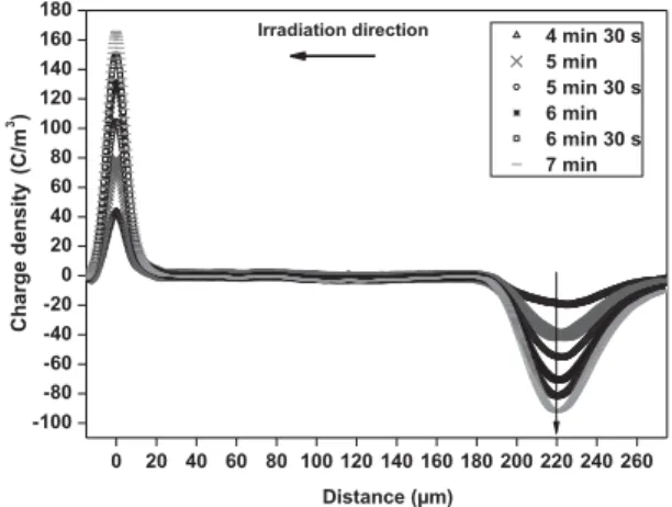
0 20 40 60 80 100 120 140 160 180 200 220 240 260 -100 -80 -60 -40 -20 0 20 40 60 80 100 120 140 160 180 Distance (m) 4 min 30 s 5 min 5 min 30 s 6 min 6 min 30 s 7 min C h ar ge density (C /m 3) Irradiation direction
Fig. 11. In-situ PEA space charge profile recorded after irradiation from 4 min 30 s to 7 min with a 30 keV electron beam energy on a PTFE sample 225 m
thick.
IV. CONCLUSIONS
In this work space charge measurements by PEA in the open configuration on PTFE irradiated sample have been realized. It has been shown that when electrons are injected near the surface the surface potential grows quickly. The risk of discharges through the specimen edge occurs as soon as a critical value, that depend on the distance between the surface and the ground, is reached. Positive charges appear at the sample surface. To prevent such unwanted phenomena, the
best solution would consist in protecting the sample edge from the irradiation with a mask during bombardment or insulate the sample for the surrounding grounded area by increasing the distances. 0 25 50 75 100 125 150 175 200 225 250 275 -120 -80 -40 0 40 80 120 160 200 Distance (m) 8 min 30 s 9 min 30 s 10 min 30 s 11 min 30 C h ar ge density (C /m 3 ) Irradiation direction
Fig. 12. In-situ PEA space charge profile recorded after irradiation from 8 min 30 s to 11 min 30 s with a 30 keV electron beam energy on a PTFE sample
225 m thick. 0 1 2 3 4 5 6 7 8 9 10 11 12 13 -28 -24 -20 -16 -12 -8 -4 0 Su rface potential (kV) Time (min)
Fig. 13. Surface potential recorded after each electronic irradiation periods of a PTFE sample 225 m thick with an energy of 30 keV.
REFERENCES
[1] V. Griseri, “Behavior of dielectric in a charging space environment and related anomalies in fight”, IEEE trans. Diel. Elec. Insul., Vol. 16, No. 3, pp. 689-695, June 2009.
[2] V. Griseri, P. Malaval, L. Berquez, T.A. Tung, S. Le Roy, L. Boudou, A. Boulanger, “Charge build-up and transport in electron beam irradiated polymers in a new irradiation chamber”, IEEE CEIDP, pp. 688-691, October 2010.
[3] T. Maeno, K. Fukunaga, “Open-PEA system for space charge measurement in dielectrics under irradiation”, 8th Int. Conf. on Solid
Dielectrics, Toulouse, France, pp. 944-946, July 5-9, 2004.
[4] C. Perrin, V. Griseri, C. Laurent, “Measurement of internal chargedistribution in dielectric using the pulsed electro-acoustic method in non-contact Mode”, IEEE Trans. Diel. E.I., Vol. 15, No. 4, pp. 958-964, August 2008.
[5] M. Wadamori, M. Fukuma, T. Maeno, K. Fukunaga and N. Nagao, “Proposal of numerical analysis model of acoustic wave propagation and generation on PEA method”, 7th Int. Conf. Properties and Applications of

![Fig. 2. In-situ PEA space charge profile recorded after various irradiation period [2-6 min] with a 30 keV electron beam energy on a PTFE sample](https://thumb-eu.123doks.com/thumbv2/123doknet/14376718.505227/3.918.91.408.88.308/charge-profile-recorded-various-irradiation-period-electron-energy.webp)
![Fig. 6. In-situ PEA space charge profile recorded after various irradiation period [18-26 min] with a 30 keV electron beam energy on a PTFE sample](https://thumb-eu.123doks.com/thumbv2/123doknet/14376718.505227/4.918.509.807.81.305/charge-profile-recorded-various-irradiation-period-electron-energy.webp)