Colloidal CdSe/CdS Nanostructures: Synthesis, Optical
Characterization and Applications
by
MA
Igor Coropceanu
B.S.
Chemistry, 2011
Georgia Institute of Technology
Submitted to the Department of Chemistry
in Partial Fulfillment of the Requirements for the Degree of
DOCTOR OF PHILOSOPHY IN PHYSICAL CHEMISTRY
at the
MASSACHUSETTS INSTITUTE OF TECHNOLOGY
September 2016
2016 Massachusetts Institute of Technology.
All rights reserved
Author...
SSACHUSETTS INSTITUTE OF TECHNOLOGYOCT 28 2016
LIBRARIES
ARHIE$
Signature redacted
0)
Department of Chemistry
Certified by...
Signature redacted
July 5, 2016
Moungi G. Bawendi
Lester Wolfe Professor of Chemistry
Accepted by...
Signature redacted
Thesis Supervisor
This doctoral thesis has been examined by a Committee of the Department of
Chemistry as follows:
Professor Troy Van Voorhis
..
Signature redacted...
Haslam and Dewey Professor of (hemstry
Chairperson
Professor Moungi G. Bawendi...Signature
redacted
Lester Wolfe Professor of Chemistry
Thesis Supervisor
Signature redacted
Professor Timothy M. Swager ....John D. MacArthur Professor
U
Colloidal CdSe/CdS Nanostructures: Synthesis, Optical
Characterization and Applications
by
Igor Coropceanu
Submitted to the Department of Chemistry
in Partial Fulfillment of the Requirements for the Degree of Doctor of Philosophy in Physical Chemistry
Abstract
The focus of this thesis is the study of CdSe/CdS nanostructures, from their fundamental properties to their integration in practical devices. This material system has proven to be remarkably robust both as a platform for studying physics in confined semiconductors, as well as for enabling various optical and optoelectronic applications. In this thesis, we will discuss our recent efforts to improve the synthesis of CdSe/CdS structures, to better understand their optical properties and to use them to create highly performing luminescent solar concentrators.
In the first part of the thesis we will discuss our efforts to improve the synthesis of CdSe/CdS nanostructures of different dimensionalities. In particular, we discuss the synthesis of CdSe/CdS quantum dots and seeded CdSe/CdS nanorods that have a near unity photoluminescence quantum yield and complete energy transfer from the shell to the core. Next, we discuss the fabrication of luminescent solar concentrators using these materials and the optical characterization of these devices. Finally, in the last section, we use a combination of synthesis, spectroscopy, and modeling to gain better insight into the photoluminescence lineshape of CdSe/CdS quantum dots.
Acknowledgements
This thesis and all the work it represents would never have been possible if it weren't for the many people in my life who have guided me and helped me along the way. I an indebted to far too many people to do this section justice, but here is a start.
I feel extremely lucky to have had the honor and pleasure of working with
Moungi Bawendi as my advisor. There are few people I have ever met who could combine such an incredibly broad base of high level knowledge with a keen critical eye towards even the smallest details. Moreover, I greatly appreciate the careful and collaborative group culture Moungi helped foster. It is hard to imagine a better atmosphere where I could learn how to do interesting and meaningful science and how to become an independent researcher.
As far as my research is concerned, I owe a debt of gratitude to the many colleagues and collaborators that I have worked with along the years. It is hard to overstate how much more I have accomplished and learned thanks to others. In particular, I have to thank Aurelio Rossinelli, Hendrik Utzat, Andrew Beyler, Thomas Bischof, Greg Gutierrez, Jian Cui, Russ Jensen, Jennifer Scherer, Justin Caram and Giovanni Azzellino.
I am also very happy to have had the chance to be part of the
spectroscopy subgroup for the past five years. Much of what I have learned at MIT has been through the many, many discussions we have had, including with Thomas, Andrew, Jian, Russ, Mark, Hendrik, Sophie, Katie, Justin, Lea, and others. Finally, I would like to thank all the other members of Bawendi Lab with whom I crossed paths over the past few years. I had a great time talking to all of you and hearing about your fascinating work spanning topics as varied as chemistry, physics and biology.
MIT. For all the great memories, both at work and outside of lab, thank you: ChiarHao, Whitney, Andrew, Jessica, Mike, Kurt, Wankyu, Jenny, Thomas, Matt, Paul, Steph, Jess, and many others. I wish you all the best and hope to see you again in the future.
Looking further back, I am very grateful for the many wonderful people at Georgia Tech who have helped me start my career as a chemist. I feel very fortunate to have had the chance of working in the lab of Seth Marder, where I got my first taste of what chemistry and real research were like. I greatly appreciate the mentorship I received along the way from Seth and the people I have worked with, especially Carlos Zuniga, Susan Odom, and Ali Hayek.
Finally, I would be more than remiss if I failed to acknowledge the great debt I owe my parents. Their support, encouragement, and guidance are what made me the person I am today, both personally and professionally. Once again, thank you very much to you all!
Table of Contents
CHAPTER 1 Introduction 17
1.1 Introduction to Quantum Confined Semiconductor Nanocrystals... 17
1.1.1 The Electronic Properties of Quantum Confined Semiconductor N anocrystals ... 18
1.2 C olloidal Nanocrystals ... 22
1.3 The Synthesis of Colloidal Nanostructures ... 23
1.4 The Fluorescence Lineshape of Colloidal Quantum Dots... 24
1.5 Lum inescent Solar Concentrators ... 28
1.5.1 Introduction ... 28
1.5.2 General Considerations for the Active Material of a Luminescent Solar C oncentrator ... 30
1.6 O verview of the T hesis ... 33
CHAPTER 2 The Synthesis and Characterization of CdSe/CdS Quantum Dots
and Nanorods
39
2.1 Thick-Shell CdSe/CdS Quantum Dots ... 412.1.1 The Evolution of the Biexciton Quantum Yield in CdSe/CdS Quantum Dots as a Function of the Shell Thickness... 43
2.2 C dSe/C dS N anorods... 44
2.2.1 Syn thesis... . . 45
2.2.2 O ptical Characterization... 50
2.2.3 Evaluation of the Shell-to-Core Energy Transfer Efficiency ... 54
2.2.4 Evaluation of the Degree of Polarization in the Fluorescence of C dSe/CdS Nanorods... 58
2.3 C onclusions... 60
2.3.1 M aterials and M ethods ... 61
2.4 Supplem entary Inform ation... 62
2.4.1 Synthesis of CdSe/CdS Quantum Dots ... 62
3.1 In trod u ction ... 75
3.2 The Use of Thick-Shelled CdSe/CdS Quantum Dots as the Active Material in Luminescent Solar Concentrators... 75
3.2.1 The Reduction of Reabsorption Using CdSe/CdS as a Host/Guest System ... . 78
3.2.2 Embedding Quantum Dots in an Optically Transparent Polymer C om posite ... 81
3.2.3 Measuring the Optical Performance of the LSC Prototypes...83
3.2.4 The Implementation of a Monte Carlo Simulation for Modeling Photon Transport in Luminescent Solar Concentrators...85
3.2.5 Determination of Fluorescence Quantum Yield of Quantum Dots in Polym er Com posites ... 89
3.2.6 C onclusions... 90
3.2.7 M ethods:... 91
3.3 Reducing Top Escape Losses in Luminescent Solar Concentrators by Aligning CdSe/CdS Nanorods ... 92
3.3.1 C onclusions... 94
CHAPTER 4 The Evolution of the Electronic and Optical Properties in CdSe/CdS Heterostructures: The Central Role of Electron Delocalization 99 4.1 Electron Delocalization into the Shell in CdSe/CdS Quantum Dots ... 100
4.1.1 Change in the Energy of the Fluorescence as a Function of the Shell Thickness in CdSe/CdS Quantum Dots... 103
4.1.2 Change in the Radiative Lifetime of CdSe/CdS Quantum Dots as a Function of the Shell Thickness... 105
4.1.3 Change in the Fluorescence Lineshape of CdSe/CdS Quantum Dots as a Function of the Shell Thickness... 108
4.1.4 Modeling of the Electron Delocalization in CdSe/CdS ... 109
4.2 Unraveling the Photoluminescence Lineshape of CdSe/CdS... 112
4.2.1 G eneral C onsiderations ... 112
4.2.2 Exciton-Phonon Coupling in CdSe/CdS... 114
4.2.3 Simulating the Spectrum of CdSe/CdS Quantum Dots: General F ea tu res ... 1 16 4.2.4 Experimental Measurement of the Temperature Dependent Fluorescence Spectra of Single CdSe/CdS/ZnS Quantum Dots... 119
4.2.5 Fitting the Experimental Temperature Dependent Data to the L ineshape M odel ... 121
4.3 Conclusions... 125
Table of Figures
Figure Figure Figure Figure Figure Figure Figure Figure Figure Figure Figure Figure1-2: The evolution of the electronic properties of an optically active material from atoms to bulk semicondcutors and modulated by quantum confinement in nanostructures ... 19
1-2: The difference between excitons in bulk semiconductors (Wannier Excitons) and Confined Excitons in Quantum Dots ... 21
1-3: General Structure of a Colloidal Core/Shell Quantum Dot ... 22 1-4: Lineshape broadening mechanisms in semiconductging nanocrystals
(adapted with permission from Ref. 14)...27
1-5: The general scheme of a solar concentrator ... 28 1-6: Basic optical processes in a luminescent solar concentrator and optical
losses (show n in red) ... 29
2-1: Type I and Quasi - Type II Core/Shell Heterojunctions; the spread of the electron wavefunction is shown in organge and the spread of the hole wavefunction is shown in blue ... 40 2-2: TEM micrograph of thick-shell Cdse/CdS quantum dots... 41
2-3: The change in the biexciton quantum yield vs. CdS shell thickness .43
2-4: The general synthetic scheme for the synthesis of the seeded nanorods
... . . 4 5 2-5: s-PCFS traces showing the ensemble and average single nanorod
spectral correlation of sam ple... 46
2-6: TEM micrograph of the nanorods after the slow-shell growth: a) a
micrograph of sample S1 d) High Resolution TEM micrograph of
sam ple S2 ... 49
2-7: a) Fluorescence spectra of the CdSe cores and the nanorods on a
linear scale and b) on a logarithmic scale... 50 2-8: Time resolved photoluminescence traces of the nanorod samples... 51
2-9: Absorption spectra of nanorods (inset magnification of first excitonic Figure
Figure Figure
Figure 2-10: Electronic processes in CdSe/CdS nanorods, including I) absorption,
II) shell-to-core energy transfer, III) fluorescence and the trapping
pathways before and after thermalization ... 54 Figure 2-11: a) Excitation-emission spectrum of CdSe/CdS nanorods (S2). b) Normalized excitation-emission spectrum of S2... 55
Figure 2-12: Excitation spectrum and absorbance of S2... 56
Figure 2-13: Fluorescence Spectrum of S2. Inset shows the weak CdS emission peak at a magnification of 10KX... 57
Figure 2-14: Schematic of the set-up used for polarization dependent single nanorod fluorescence spectroscopy b) Fluorescence intensity of sample T1 as a function of the polarizer angle... 59
Figure 3-1: Use of CdSe/CdS quantum dots as a host/guest system. The key optical properties start with I) absorption by the shell material (the antenna), II) energy transfer to the core (the guest) and III) radiative recom bination from the core ... 76
Figure 3-2: TEM micrograph of the CdSe/CdS quantum dots used for the LSCs ... . . 7 7 Figure 3-3: Evolution of the absorption spectra as a function of the shell volume (x refers to the volumetric ratio of the shell material relative to the thinnest shell studied) ... 78
Figure 3-4: Optical spectra of the thick-shelled CdSe/CdS quantum dots on a linear scale (left) and a logarithimic scale (right)...79 Figure 3-5: Definition of the reabsorption figure of merit S ... 80
Figure 3-6: Reduction of reabsorption as a function of the shell thickness...80 Figure 3-7: General schematic of the
cuvette
used to fabricate the composites(left) and the cuvette in use (right) ... 81
Figure 3-8: Absorption spectrum of the CdSe/CdS dots in solution and in the PLMA matrix; inset: a close-up of the spectral region from 500-800n m ... . . 82
Figure 3-9: The LSC prototype and the set-up for the optical measurements; Left panel: basic scheme for optical efficiency measurements; Right panel: QD/polymer composites in ambient light (left) and under UV
illumination (right) with the edges clear (top) and blocked by carbon pain t (bottom ) ... 83
Figure 3-10: EQE spectra of the LSC prototype (left) and optical efficiency of the
L SC (right)... . 84
Figure 3-11: Schematic of the Monte Carlo Simulation for Photon Transport in the Luminescent Solar Concentrator... 85
Figure 3-12: Distribution of outcomes for photons incident on the LSC from the M onte Carlo sim ulation... 88
Figure 3-14: The vertically aligned packed CdSe/CdS; a) optical image; b) TEM micrograph with the inset showing the Fast Fourier Transform (F F T )... . . 9 3
Figure 4-1: The band alignment in CdSe/CdS; a) a band edge electron (red) and a band-edge hole (blue); b) the spatial extent of the electron and hole wavefunctions; c) uncertainty in the band offset of the CdSe and CdS conduction bands ... 100
Figure 4-2: The central role of electron delocalization in shaping the electronic and optical properties of CdSe/CdS... 101
Figure 4-3: The evolution of the fluorescence peak of a series of CdSe/CdS dots with a core with a first excitation feature at 563nm ... 102 Figure 4-4: The evolution of the fluorescence maximum vs shell thickness (a) and the relative change in the fluorescence maximum for each step of the shell grow th (b )... 103
Figure 4-5: Normalized time-resolves photolumienscence of a series of CdSe/CdS dots, using a core with a first absorption feature at 605nm ... 107 Figure 4-6: Evolution of the PL lifetime in CdSe/CdS QDs vs the shell volume for 3 different core sizes... 107
Figure 4-7: Evolution of the FWHM of the fluorescence spectrum of CdSe/CdS QDs vs the shell volume for 3 different core sizes ... 108
Figure 4-8: The evolution of the radial distribution function (RDF) for the electron in CdSe/CdS as a function of the shell thickness for a) no Coulomb potential and b) in the presence of a Coulomb potential and
---Figure 4-9: The eight band-edge fine structure states in spherical wurtzite CdSe quantum dots vs. Q D radius... 113
Figure 4-10: The phonon progression of a two-level system coupled to one phonon mode with Energy ELO ..---...---.-.... 115
Figure 4-11: Simulations of the fluorescence lineshape at: a) 4K with no linear temperature dependence, g1=g2=0.06, g3=0.6; b) 300 K with no linear temperature dependence, g1=g2=0.06, g3=0.6; c) 300 K with a linear temperature dependence, g1=g2=0.06, g3=0.6; d) 300 K... 118 Figure 4-12: The Emission Spectra of Sample IC-I-95 plotted in absolute energy (top) and difference from peak energy (bottom) ... 120 Figure 4-13: The evolution of the photoluminescence lineshape from 5K to 60K
... 1 2 3
Figure 4-14: The evolution of the photoluminescence lineshape from 100K to 2 80 K ... 12 4 Figure Al: The configuration used to measure the quantum yield ... 130
CHAPTER 1
Introduction
1.1 Introduction to Quantum Confined Semiconductor Nanocrystals
Quantum confined nanocrystals are a class of semiconducting structures which are defined by the property that their physical shape and size strongly modulate their electronic structure. Typically, at least one or more dimensions of these structures lie on the scale of 1-100nm as implied by their name. The broader family of nanocrystals includes spherical (quasi 0-dimensional) structures called quantum dots, elongated (quasi 1-deminsional) structures called nanorods or nanowires and pancake-like (quasi 2-dimensional) structures called nanoplatelets. Due to their strong quantum confinement, nanocrystals offer a broad range of tools through which their electronic, optical, and chemical properties can be tuned. Through a judicious choice of the semiconducting material(s), the architecture of structure, as well as its size and shape, the spectral region in which the structure is optically active can be tuned from the near-ultraviolet (near-UV) to the mid infrared (MWIR). This high degree of flexibility, coupled with the possibility of narrow emission bands and near unity quantum yields have made quantum dots an appealing system for a variety of applications, ranging from optoelectronics to biological imaging. 14
1.1.1 The Electronic Properties of Quantum Confined Semiconductor
Nanocrystals
The general behavior of the electronic properties of quantum dots and related nanostructures is succinctly summarized by their definition as "spatially confined semiconductors". As this wording suggests, two key aspects dominate the electronic property of these structures: 1) their material composition and 2) their specific size and shape. The first of these factors is well understood within the framework of solid state semiconductor physics. Beginning with the discrete orbitals of atoms, one can then build up larger and larger structures, going from molecules, to small clusters, until one reaches the bulk limit, as summarized in Fig. 1-1. At the bulk level the electronic structure is best understood by transitioning from a discrete picture of energy levels, to a quasi-continuum picture of energy bands with an associated density of states. A key property of optically active semiconductors is the presence of energy separation between the highest occupied band (the valence band) and the lowest unoccupied band (the conduction band) called the bandgap.
This bulk picture can conveniently be taken as the starting point for evaluating the electronic structure of spatially confined semiconductors. A powerful theoretical tool to study the transition from the bulk limit to the confined case is the effective mass approximation (EMA).5 The result of this mathematical treatment is to combine the periodic Bloch functions of the bulk crystal with an additional function called the envelope. The envelope captures the effect of the shape and size of the nanostructure in shaping the new set of wavefunctions describing the system.
5-rnd C ion ...
Bn
____ Band Bandgap ... . ...---... W e c ...4
Atoms
Molecules
Clusters
Bulk
Semiconductor
[igive 1-I le eVOiution of tIe elect roil Ic pio pe ies of l] op ticalIl Ictive
inaterIal f'r om atomS to Iu1k se riC)!)dcu1o s t( d s Iodulated by atia- 11n-1
C)Onfiiernent, ill nlanosrl 1 t u[es
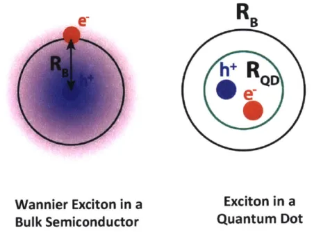
The opticzl properties of Uantfnltrn Confined ]n oCrystis is us ost, colillonlY mediated bY bound eleCtriio-iole pails. called I bulk CTySta.ls an (d witLin the CffeCtive mi app[oxiiima ti tle excitofi cafn be described as a,
bYdrogen-like system where tOI eleCton is euCtrostatIcal l hotid L the hole.
Si ililax to the Case of tIe vydr )eC atom, we can define a q untitv cal led the 1Bolr radius of the excii) (P ) as defined in CCquathiu 1-1 ]elow
RB = Er ~~a 0 (1-I) u) Lu Effective Bandgap
0
Quantum
Dots
where
Er
is the dielectric constant of the semiconductor, me is the free electron mass, p* is the reduced effective mass of the exciton, and ao is the Bohr radius of a hydrogen atom.The Bohr radius can be taken as a natural reference point to study the degree of quantum confinement in such a system (see Fig. 1-2). In bulk semiconductors and large micro-crystallites the size of the crystal (rQD) is much
larger than the excitonic Bohr radius (RB). In these systems the Wannier basis provides a natural description of the electronic structure of excitons, with the physical confinement of the nanostructure acting at most as a perturbation. On the other hand, as the particle of nanocrystal decrease, its spatial confinement will add a repulsive energy term called the confinement energy (Econfinement),
which for a spherical particle varies inversely with the square of its radius:
h21r2
Econfinement = 2Ip*r2
(1-2)
For a semiconducting particle subjected to strong confinement of its charge carriers, it is often convenient to separate the energy of the exciton according the various contributing sources. Following the EMA formalism introduced above, the energy of the exciton can be expressed as the sum of three terms: 1) the bandgap of the bulk material, the confinement energy of the exciton as defined above, and finally the Coulomb attraction between the two charge carriers (Eq. 1.1).
Eexciton = Ebandgap + Econfinement + Ecoulomb
(1-3)
RB
Wannier Exciton in a
Bulk Semiconductor
RB
h+ R
QD
Exciton in a
Quantum Dot
Figure 1-2: The difference between excitons in bulk serniconductors1.2 Colloidal Nanocrystals
Nanocrvstals of' difTerent (i viieilsionalities can be grown using a variety of
techniques, including gas-phase, iqu(id-phiase, anvd solid-phase approaches. In this
work, the focus will he on nanocrystals grown through self-assenbly in solition. These growth conditions generally allow the particles to torm stable coI loi(ial suspension s in a cornpatible solvent, giving rise to the termi "colloidal
nanocrystal." Because of their growth conditions, colloidal nanocrystals consist of both an inorganic part and an organic exterior.
Figii re 1-3 below shows the architecture of a typical colloidal
nanostructure: a core shell quantum (lot. In this structure., an inorganic core is
surrounded by an additional inorganic layer called the shell. The shell in turn is surrounded by a laver of organic ligands, whici ensure the cotloidat stabiltv of'
the structui. In practice, the details of the inorganic part of the nanocrystal can vary drastically, including the possibility of a single inorganic layer, complicated multilaver structures, or graded alloyed striictures. Likewise, the ligand shell can
Shell
Ligands
Figure 1-3: General Structure of a, Colloidal Core Shell
range from simple short chain organic moieties (e.g. carboxylic acids, amines, thiols) to more complex scaffolds such as multifunctional block copolymers. It is important to emphasize that while a primary role of the ligand shell is to render the nanocrystal soluble in a solvent of choice, it can also play an important functional role, including by directly affecting the electronic properties of nanostructure as a whole.
1.3 The Synthesis of Colloidal Nanostructures
Since the first reports of the successful solution based synthesis of colloidal quantum dots, dramatic progress has been made in improving the synthetic quality and expanding the complexity of such structures. The most widely used method to create monodisperse batches of quantum dots remains the hot-injection technique. In this method, the precursors of the quantum dot material are allowed to quickly react together in a well-defined nucleation step, followed
by a secondary growth step. As a result of the tendency of small particles to grow
more quickly than larger particles, it is possible for the growth step to occur in a regime called "size focusing," where the size distribution of the quantum dots can narrow.9 As a result, for many classes of materials it is possible to reproducibly obtain batches of nanorods with very low polydispersity (often less than 5%).2
While early studies of quantum dots focused on single-material systems, the field was rapidly expanded by the development of multilayer structures.10 The simplest example of such heterostructures are core/shell quantum dots, such as the one shown in Fig. 1-3 above. It soon became apparent that core/shell quantum dots could offer key advantages over core only dots, especially for luminescent applications. Key among these benefits were a high quantum yield, low emission intermittency (blinking), and improved photostability.2, 1 Other possibilities included changing the shape of the particle by embedding the spherical core in a shell that was elongated as in seeded nanorods or which had
1.4 The Fluorescence Lineshape of Colloidal Quantum Dots
One of the most important properties that characterize a semiconducting nanocrystal is the structure of the fluorescence lineshape. Controlling the lineshape is crucial for enabling the use of such nanostructures as fluorophores in applications ranging from light emitting diodes to multiplexed imaging. Moreover, from a fundamental perspective the lineshape, including its breadth and structure, provides critical information on the electronic structure of the nanocrystal and the key physical processes that modulate its dynamics.
One of the most attractive features of quantum dots and related nanostructures is that they exhibit a narrow and tunable emission band. However, the word "narrow" merits a more careful look in this context. High quality nanostructures based on a spherical CdSe core generally have a PL lineshape with a full width at full max (FWHM) on the order of 60-80meV (~20nm at an emission maximum of 630nm).2, 14, 15 From an application standpoint, this lineshape very often compares very favorably to alternative chromophores. For example, for light emitting applications, the narrow lineshape of CdSe based quantum dots is substantially narrower than the corresponding emission bands of typical organic phosphors used in the display industry. As a result, new displays incorporating quantum dots are capable of producing a higher color purity than that found in older generation LCD displays.16
Nevertheless, while the lineshape of quantum dots can be considered to be narrow for many practical applications, from a physical perspective it appears to be unexpectedly broad at first sight. As a starting point, we can calculate the "natural" lineshape of the quantum dots (6Enat) if the only broadening mechanism was due to its finite radiative lifetime (Tad), which can be expressed as in Eq. 1-3 below:
h MEnat = 2
lThrad
(1-4)
Taking into account the fact that the radiative lifetime of CdSe quantum dots is typically on the order of -10 ns, we obtain a natural linewidth on the order of
100 neV.
Clearly this number is smaller by many orders of magnitude when compared to the lineshape observed at room temperature. The question then becomes what mechanism dominates the broadening. At the individual dot level, possibilities include 1) spectral dynamics induced by the fluctuating environment of the dots, 2) the presence of multiple emissive states, and finally, 3) the presence of exciton-phonon coupling.14' 17' 18 These three factors together define the average single-particle lineshape. In addition to these mechanisms, the polydispersity of the quantum dot sample will also add a contribution to the lineshape measured at the ensemble level, which we will call the inhomogenous broadening. All the four mechanisms described above are shown pictorially in Fig. 1-4.
A key question is what mechanism dominates the broadening that results
in the room temperature spectrum? The first part of the answer as it relates to CdSe/CdS quantum dots is that size inhomogeneity is not the answer. A variety of techniques ranging from single particle fluorescence to solution - photon correlation Fourier spectroscopy (s-PCFS) indicate that for high quality batches of CdSe/CdS dots the average single particle spectrum is alost identical to the ensemble spectrum.2, is As a result, the broad ensemble lineshape simply reflects the fact that each individual quantum dot has a spectrum that is broad.
studies we know that the net effect of spectral diffusion is to induce broadening on the order of less than 1meV, particularly for thicker core/shell particles.18
This fact is consistent with our observations that the room temperature spectrum of these particles is effectively constant when monitored on timescale accessible on a camera (10s of ms). Next we can turn to the effect of the exciton fine structure. In CdSe/CdS dots, the only states that have a non-zero oscillator strength and can be thermally populated (at room temperature) have an energy difference of 10-20meV.1 4 While this fine structure can clearly have an important impact on the overall lineshape, it cannot by itself account for the 60-100meV linewdiths observed in practice.
The last key mechanism that remains to be explored is exciton-phonon coupling. In previous studies, coupling to phonons has been invoked as the key meenaism dominating the broadening of the lineshape.' 4, 9 While this conclusion is reasonable from the available data, the key limitation of the available studies is that they could only rely on indirect evidence to attribute the broadening to exciton-phonon coupling. In Ch. 4 we will discuss a more direct approach to quantifying this coupling by measuring the fluorescence spectra of CdSe/CdS quantum dots at the single particle level from cryogenic temperatures (4K) all the way to room temperature.
In homogeneously-Broadened
Ensemble Spectrum
Size
Inhomogeneity
Single-Nanocrystal Spectrum/
Spectral Dynamics P1I
AI
iL
honon Coupling Exciton Fine Structure
t
/
Lb
Lifetime-Limited "Natural" Spectrum
Figure
1-
1:1lneshape
broadening nechanisrns in seiconductging nan crystalsm
1.5 Luminescent Solar Concentrators
1.5.1 Introduction
Luminescent solar concentrators (LSCs) have emerged in recent years as a promising avenue towards economically viable solar energy harvesting.2 0 2' As in
all other types of solar concentrators, the key operating principle of an LSC is the collection of light over a large surface area and its concentration to a, target with a, smaller surface area. In contrast to conventional (active) solar concentrators, which rely on direct focusing of the light (e.g. using parabolic mirrors or troughs), LSCs are a passive system that does not require active tracking of the Sun.2 In an LSC concentration is achieved by relying on a. chromophore embedded in a dielectric slab to first absorb the incoming solar radiation and then to re-emit the light. The slab then acts as a waveguide, which traps part of the emitted flux through refractive index contrast and guides it to the edges (see Fig 1-6). The ratio of the surface area of the face of the device to the surface area of the edges then defines the geometric concentration factor called the concentration gain, siunilar to a conventional concentrator. A solar cell can then be placed at the edges to carry out the final conversion of the light to electricity.
Light Collector
Solar Cell
Geometric Gain: G
AqijetA target
Their passive mode of operation allows LSCs to not only avoid expensive solar tracking controllers, but also offers the benefit of collecting both direct and diffuse sunlight. As a result, LSCs offer the possibility of creating a more cost-effective and efficient platform for solar energy harvesting, which can be coupled to existing PV systems. Nevertheless, for the practical implementation of such devices, further improvements are required, most notably in increasing the proportion of the incident photon flux successfully collected and guided to the edges. Their high photoluminescence quantum yield, strong and broad absorption, and versatile tunability have made nanocrystalline structures such as quantum dots and nanorods promising candidates to serve as the active material in LSCs. One advantage of nanorods is the possibility of creating core-shell structures, which allows a, spectral separation of the absorption and emission, thus diminishing reabsorption. Furthermore, because of their anisotropic shape, nanorods can preferentially emit light in a, plane perpendicular to their long axis , a property which can lead to a reduction in top escape losses if the nanorods are aligned perpendicular to the plane of the concentrator.2 6
Incident Solar Light
op Escape
SRea
I
Polymer Matrix
Solar Cell
Emitter
(Core/Shell Quantum Dots)
Figure 1-6: Basic optical processes in a luminescent solar concentrator and optical losses (shown in red)
1.5.2 General Considerations for the Active Material of a Luminescent
Solar Concentrator
A key figure of merit describing the performance of luminescent solar
concentrators is the optical efficiency rq, defined as the ratio of the photon flux guided to the edges of the LSC divided by the incident flux. This quantity scales approximately as:
?7(A)~A(?7P1?7t.)n"1
(1-5)
In the equation above, A is the fraction of photons absorbed, r7p, and 7t,. are the photoluminescence efficiency and trapping efficiency (the fraction of photons re-emitted in the LSC trapped via total internal reflection) respectively, and n is the number of reabsorption events.2 7 A key consequence of the above relationship is
that unless the two internal efficiencies reach unity, a situation extremely difficult to realize in practice, the optical efficiency will rapidly decrease with the number of reabsorption events. This latter issue is particularly problematic since for LSCs to have practical applications, a large geometric gain, G (the ratio of the area of the face of the LSC to the surface area of the edges), is needed.
The requirement for a large geometric gain arises from the dependence of the ability of an LSC to concentrate light on this parameter. Specifically, the amount of light concentrated can be quantified by F, the so-called flux gain, defined as the ratio of the photon flux guided to the edges divided by the solar energy flux that would be incident on the surface area of the edges, which can be expressed as F = il x G. From this relationship, it is immediately clear that an
LSC cannot significantly concentrate light unless it has a large geometric gain.
However, as the geometric gain increases, so necessarily does the average optical path of the light through the device, thus increasing the probability for
reabsorption and diminishing the efficiency, such that at a certain value of G the flux gain will stop rising.
For the above-mentioned reasons, reducing the reabsorption has always been the key problem in LSC development and numerous solutions to this problem have been explored. Most of the strategies pursued to this end can generally be divided into two classes 1) changes in intrinsic material parameters to reduce the spectral overlap between the absorption and emission and 2) dilution of the emissive species.24 The most notable approach belonging to the first category is the energetic separation of the positions of the absorption and emission maxima corresponding to the same electronic transition, e.g. due to vibronic coupling. For organic dyes this value is usually equal to the Stokes shift, the energy difference between the global absorption and emission maxima. However, in spite of extensive efforts to screen possible candidate materials exhibiting a sufficiently large Stokes shift for LSC applications, even the best materials display significant reabsorption relying on this factor alone.
A related strategy, called solid state solvation (SSS), is based on the
preferential stabilization of the excited state in a polar solid matrix, resulting in a further reduction in reabsorbance. It was on a combination of a large Stokes shift organic dye and exploitation of SSS that a state-of-the-art LSC developed by Baldo and coworkers was based.20 An additional approach in this category is reliance on emission via an electronic transition with a low absorption oscillator strength, such as emission from phosphorescent complexes or f-f transitions in rare earth complexes.20, 28 However, while such materials have indeed been proven to yield greatly diminished reabsorption, their applicability to LSCs has generally been limited either by a low quantum yield or insufficient absorption across the solar spectrum.
a blend of separate components or a single material containing two separate subunits. In terms of the former, various systems composed of an organic host and a fluorescent or phosphorescent guest have been reported.20, 29 One approach falling into the latter category is based on the use of core-shell inorganic nanorods. In such systems, emission occurs exclusively from the core, while the majority of the absorption takes place in the shell. The key to minimizing reabsorption in such systems then is essentially to minimize the volume ratio of the core to the shell. In Ch. 4 we will discuss the realization of this approach using CdSe/CdS quantum dots and nanorods to create an active material with minimal reabsorption and near unity fluorescence quantum yields.
1.6 Overview of the Thesis
The thesis focuses on the synthesis, characterization, and application of semiconducting nanocrystals. In particular, the material system studied consisted of core/shell structures of CdSe/CdS having either a spherical CdS shell
(quantum dots) or an elongated shell (nanorods).
Chapter 2 discusses the development of new methods to synthesize CdSe/CdS core/shell quantum dots and nanorods. The characterization of the materials using a suite of optical tools ranging from spectrophotometry to single particle fluorescence is discussed. In particular, we emphasize the key factors needed obtain particles with a quantum yield approaching 100% and complete energy transfer from the shell to the core.
Chapter 3 deals with the study of the active materials used in luminescent solar concentrators. Inorganic heterostructures are shown to be ideally suited to reduce reabsorption due to their ability to act as a host/guest system where one part of the structure is responsible for the absorption and another part is responsible for the emission. The fabrication, optical characterization, and modeling of prototype devices fabricated using CdSe/CdS quantum dots is discussed in detail.
Chapter 4 discusses the optical and electronic properties of CdSe/CdS quantum dots. The role of electron delocalization into CdS is discussed as the central mechanism directing the evolution of the optical spectra as a function of the shell thickness. A unified model is presented to describe the fluorescence lineshape in these particles and its dependence on exciton-phonon coupling in the quantum dots.
Ch. 1 References
1. Mashford, B. S.; Stevenson, M.; Popovic, Z.; Hamilton, C.; Zhou, Z.; Breen, C.; Steckel, J.; Bulovic, V.; Bawendi, M.; Coe-Sullivan, S.; Kazlas, P. T. High-Efficiency Quantum-Dot Light-Emitting Devices with Enhanced Charge Injection. Nat Photon 2013, 7, 407-412.
2. Chen, 0.; Zhao, J.; Chauhan, V. P.; Cui, J.; Wong, C.; Harris, D. K.; Wei,
H.; Han, H. S.; Fukumura, D.; Jain, R. K.; Bawendi, M. G. Compact High-Quality Cdse-Cds Core-Shell Nanocrystals with Narrow Emission Linewidths and Suppressed Blinking. Nat. Mater. 2013, 12, 445-451.
3. Castelli, A.; Meinardi, F.; Pasini, M.; Galeotti, F.; Pinchetti, V.; Lorenzon, M.; Manna, L.; Moreels, I.; Giovanella, U.; Brovelli, S. High-Efficiency All-Solution-Processed Light-Emitting Diodes Based on Anisotropic Colloidal Heterostructures with Polar Polymer Injecting Layers. Nano Lett. 2015, 15, 5455-5464.
4. Han, H.-S.; Niemeyer, E.; Huang, Y.; Kamoun, W. S.; Martin, J. D.; Bhaumik, J.; Chen, Y.; Roberge, S.; Cui, J.; Martin, M. R.; Fukumura, D.; Jain, R. K.; Bawendi, M. G.; Duda, D. G. Quantum Dot/Antibody Conjugates for in Vivo Cytometric Imaging in Mice. Proceedings of the National Academy of Sciences 2015, 112, 1350-1355.
5. Efros, A. L.; Rosen, M. The Electronic Structure of Semiconductor Nanocrystals. Annual Review of Materials Science 2000, 30, 475-521.
6. Efros, A.; Rodina, A. Band-Edge Absorption and Luminescence of Nonspherical Nanometer-Size Crystals. Physical Review B 1993, 47, 10005-10007.
7. Efros, A. L.; Rosen, M.; Kuno, M.; Nirmal, M.; Norris, D. J.; Bawendi, M. Band-Edge Exciton in Quantum Dots of Semiconductors with a Degenerate
Valence Band: Dark and Bright Exciton States. Physical Review B 1996, 54, 4843-4856.
8. Murray, C. B.; Norris, D. J.; Bawendi, M. G. Synthesis and Characterization of Nearly Monodisperse Cde (E = Sulfur, Selenium, Tellurium) Semiconductor Nanocrystallites. J. Am. Chem. Soc. 1993, 115, 8706-8715.
9. Thanh, N. T. K.; Maclean, N.; Mahiddine, S. Mechanisms of Nucleation and Growth of Nanoparticles in Solution. Chem. Rev. (Washington, DC, U. S.) 2014, 114, 7610-7630.
10. Carbone, L.; Cozzoli, P. D. Colloidal Heterostructured Nanocrystals: Synthesis and Growth Mechanisms. Nano Today 2010, 5, 449-493.
11. Ghosh, Y.; Mangum, B. D.; Casson, J. L.; Williams, D. J.; Htoon, H.; Hollingsworth, J. A. New Insights into the Complexities of Shell Growth and the Strong Influence of Particle Volume in Nonblinking "Giant" Core/Shell Nanocrystal Quantum Dots. J. Am. Chem. Soc. 2012, 134, 9634-9643.
12. Carbone, L.; Nobile, C.; De Giorgi, M.; Sala, F. D.; Morello, G.; Pompa, P.; Hytch, M.; Snoeck, E.; Fiore, A.; Franchini, I. R.; Nadasan, M.; Silvestre, A. F.; Chiodo, L.; Kudera, S.; Cingolani, R.; Krahne, R.; Manna, L. Synthesis and Micrometer-Scale Assembly of Colloidal Cdse/Cds Nanorods Prepared by a Seeded Growth Approach. Nano Lett. 2007, 7, 2942-2950.
13. Talapin, D. V.; Nelson, J. H.; Shevchenko, E. V.; Aloni, S.; Sadtler, B.; Alivisatos, A. P. Seeded Growth of Highly Luminescent Cdse/Cds Nanoheterostructures with Rod and Tetrapod Morphologies. Nano Lett. 2007, 7,
2951-2959.
14. Cui, J.; Beyler, A. P.; Coropceanu, I.; Cleary, L.; Avila, T. R.; Chen, Y.; Cordero, J. M.; Heathcote, S. L.; Harris, D. K.; Chen, 0. Evolution of the Single-Nanocrystal Photoluminescence Linewidth with Size and Shell: Implications for
Exciton-Phonon Coupling and the Optimization of Spectral Linewidths. Nano Lett. 2015, 16, 289-296.
15. Cui, J.; Beyler, A. P.; Marshall, L. F.; Chen, 0.; Harris, D. K.; Wanger,
D. D.; Brokmann, X.; Bawendi, M. G. Direct Probe of Spectral Inhomogeneity
Reveals Synthetic Tunability of Single-Nanocrystal Spectral Linewidths. Nature Chem. 2013, 5, 602-606.
16. Chen, 0.; Wei, H.; Maurice, A.; Bawendi, M.; Reiss, P. Pure Colors from Core-Shell Quantum Dots. MRS Bulletin 2013, 38, 696-702.
17. Empedocles, S. A. Quantum-Confined Stark Effect in Single Cdse Nanocrystallite Quantum Dots. Science 1997, 278, 2114-2117.
18. Beyler, A. P.; Marshall, L. F.; Cui, J.; Brokmann, X.; Bawendi, M. G. Direct Observation of Rapid Discrete Spectral Dynamics in Single Colloidal Cdse-Cds Core-Shell Quantum Dots. Phys. Rev. Lett. 2013, 111, 177401.
19. Salvador, M. R.; Graham, M. W.; Scholes, G. D. Exciton-Phonon Coupling and Disorder in the Excited States of Cdse Colloidal Quantum Dots. The Journal of Chemical Physics 2006, 125, 184709.
20. Currie, M. J.; Mapel, J. K.; Heidel, T. D.; Goffri, S.; Baldo, M. A. High-Efficiency Organic Solar Concentrators for Photovoltaics. Science 2008, 321,
226-228.
21. Bronstein, N. D.; Li, L.; Xu, L.; Yao, Y.; Ferry, V. E.; Alivisatos, A. P.; Nuzzo, R. G. Luminescent Solar Concentration with Semiconductor Nanorods and Transfer-Printed Micro-Silicon Solar Cells. ACS Nano 2013, 8, 44-53.
22. Brovelli, S.; Schaller, R. D.; Crooker, S. A.; Garcia-Santamaria, F.; Chen, Y.; Viswanatha, R.; Hollingsworth, J. A.; Htoon, H.; Klimov, V. I. Nano-Engineered Electron-Hole Exchange Interaction Controls Exciton Dynamics in Core-Shell Semiconductor Nanocrystals. Nat. Commun. 2011, 2, 280.
23. Coropceanu, I.; Bawendi, M. G. Core/Shell Quantum Dot Based Luminescent Solar Concentrators with Reduced Reabsorption and Enhanced Efficiency. Nano Lett. 2014, 14, 4097-4101.
24. Debije, M. G.; Verbunt, P. P. C. Thirty Years of Luminescent Solar Concentrator Research: Solar Energy for the Built Environment. Adv. Energy Mater. 2012, 2, 12-35.
25. Hu, J. Linearly Polarized Emission from Colloidal Semiconductor Quantum Rods. Science 2001, 292, 2060-2063.
26. McDowall, S.; Johnson, B. L.; Patrick, D. L. Simulations of Luminescent Solar Concentrators: Effects of Polarization and Fluorophore Alignment. J. Appl. Phys. 2010, 108, 053508.
27. Mulder, C. L.; Reusswig, P. D.; Velazquez, A. M.; Kim, H.; Rotschild, C.; Baldo, M. A. Dye Alignment in Luminescent Solar Concentrators: I. Vertical Alignment for Improved Waveguide Coupling. Opt. Express 2010, 18, A79-A90.
28. Wang, T.; Zhang, J.; Ma, W.; Luo, Y.; Wang, L.; Hu, Z.; Wu, W.; Wang, X.; Zou, G.; Zhang,
Q.
Luminescent Solar Concentrator Employing Rare Earth Complex with Zero Self-Absorption Loss. Solar Energy 2011, 85, 2571-2579.29. Botta, C.; Betti, P.; Pasini, M. Organic Nanostructured Host-Guest Materials for Luminescent Solar Concentrators. Journal of Materials Chemistry A
CHAPTER 2
The Synthesis and Characterization of CdSe/CdS
Quantum Dots and Nanorods
From the very beginning of the field of colloidal quantum dots, the material CdSe has played a central role in the field. Fundamental studies of CdSe nanocrystals were critical in unraveling the complex behavior of quantum dots, from their general electronic structure to the dynamics of single particles.1, 2 Likewise, it was CdSe that opened the gates to a variety of practical applications of quantum dots in areas such as biological imaging and electroluminescent devices.3 This entire body of work was made possible by a series of synthetic advances which produced particles which were: 1) uniform at the batch level, 2) tunable in size and shape, and 3) exhibited a high fluorescence quantum yield and 4) exhibited long-term photostability. 1'4'
Early in the development of colloidal quantum dots, it became apparent that the optical quality of the structures could be improved by surrounding the original dot (now called the core) with a second inorganic layer (called the shell).6 For luminescent applications the most important role of the shell is to help confine the exciton in and around the core and to protect it from defects and perturbations on the surface. The requirement to confine the exciton close to the core dictates that as a prerequisite the shell must have a higher band gap
that both the conduction and valence bands of the shell material lie higher in energy than the corresponding bands in the core material.
This situation is shown diagrammatically in Fig 2-1 below. The strongest confinement occurs when a high band offset exists for both the conduction and valence bands, called a type-I heterojunction. For example, in the case of CdSe, such an arrangement can be achieved when overcoating the core with a material such as ZnS.7 In contrast, if one of the bands of the shell
lies
close in energy to the corresponding band in the core, one can achieve what is called a quasi - type-II hand alignment. For example, in the case of CdSe, such an arrangement isfound
when CdS is used as the shell material. In this case, the low barrier between the conduction bands allows for significant electron delocalization into the shell.'' " The implication of this delocalization fIr the electronic and optical properties of CdSe/CdS nanostructures is discussed in detail in Ch. 4.'3)
Type I
Quasi
-Type II
Figure 2-1: Type I and Quasi - Type II Core/Shell Heterojunctions; the spread of the electron wavefunction is shown in organge and the spread of
2.1 Thick-Shell CdSe/CdS Quantum Dots
Of all the shell nmaterials used to overcoat (dSe quantum dots, CdS has
been rermarkable successful in creating heterostructures with superlative )ptical
properties. The CdSe"CdS system has produced particles with unity fluorescence quanUim Yields, high 1iexci ton quantumnr yields, mii I I nmal in ho mn ogen leouIs
broadening, and highly suppressed blinking. 4. !-413 Diie to these properties,
(dSe (CdS quanturm dots have been i ntegrated into a wide variety of applications, ranging frorn
light
em
itting devices, biological inaging, and otheroptical and optoelectronic appicatioiis. 14. 15
The versatility of CdSe based quantun (lots has been drarnatically expanded recent synthetic advarices in the growth of a thick CdS shell. Stich thick-shell CdSe CdS dots can now be grown while retaining a high degree of
monodispersity at the batch level, near unity quantum yields, and narrow fluorescence lineshapes. These thick-shelled particles have proven especially attractive for applications that require minimal reabsorption, such as luminescent solar concentrators and to a lesser degree in displays. 0' 16 The reduction in reabsorption is made possible by effectively decoupling the absorption and emission of these particles. While high energy light will mostly be absorbed into the shell, the exciton created in this process will rapidly relax in energy and localize in the core, where it can finally recombine radiatively. This idea will be discussed in more detail in the next chapter.
While numerous methods exist to grow the CdS shell on these particles, the best results have been obtained using a slow-injection high temperature growth that has previously been reported4 and which we adapted for thick-shell CdSe/CdS dots. Two of the biggest advantages of this method is that it yields particles with a high degree of uniformity at the batch scale (e.g. see Fig. 3-3) and near unity quantum yields. These advantages appear to follow from the high degree of crystallinity of the shell which reduces the number of non-radiative channels that otherwise can reduce the quantum yield. The benefit of this passivation scheme is especially striking for particles with very thick shells (15+ monolayers of CdS). In these particles, electron delocalization into the shell results in a dramatic lengthening of the radiative lifetime (from ~20 ns to hundreds of ns). Nevertheless, because the non-radiative decay channels are so efficiently suppressed, the radiative pathways can still dominate, allowing from fluorescence quantum yields up to 100%.
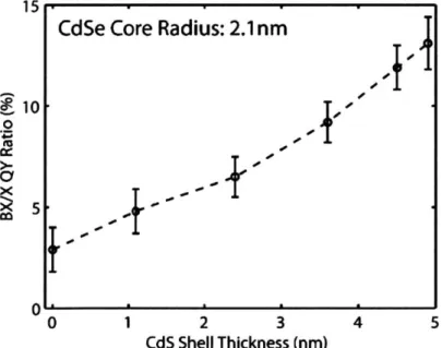
2.1.1 The Evolution of the Biexciton Quantum Yield in CdSe/CdS
Quantum Dots as a Function of the Shell Thickness
As another illustration of the benefit of the shell in CdSe/CdS heterostructures, we have looked at the evolution of the biexciton quantum yield. In core only CdSe or related system, the biexciton quantum yield is generally no higher than ~3%. 1 1 This low quantum yield is generally attributed to
Auger-mediated non-radiative relaxation of the biexciton to the exciton.17 1 Because the Auger process depends on the wavefunction overlap of the core and electron wavefunction, its rate can be inhibited by increasing the separation between the two charge carriers. 11 "1, 14 Indeed, when looking at a series of CdSe/CdS quantum dots one observes a, monotonic increase in the biexciton quantum yield as seen in Fig 2-3. In fact, by using an extension of this approach combined with partial alloying, more reont studies have demonstrated that that the biexciton quantum yield can even be made to reach unity.13
15
CdSe Core Radius: 2.1 nm
10
0
0 12 3 4 5
CdS Shell Thickness (nm)
2.2 CdSe/CdS Nanorods
The versatility of inorganic nanocrystals is greatly expanded by the possibility of modifying their electronic properties by changing not only their size, but also their dimensionality. In particular, elongated structures such as nanorods exhibit an attractive set of emergent properties that set them apart from spherical quantum dots, such as a large degree of fluorescence anisotropy20
21 and enhanced transport through various types of biological tissue 22.
Among visible-light emitting materials, seeded CdSe/CdS nanorods (structures consisting of a spherical CdSe core surrounded by an elongated CdS shell) have emerged as a robust material system combining a high degree of monodispersity with bright and spectrally narrow photoluminescence. However, while rapid initial progress in the development of CdSe/CdS nanorods resulted in the achievement of fluorescence quantum yields of up to 75%20, 23, further improvement of the quantum yield proved elusive using conventional fast-injection based preparations. Moreover, as with CdSe/CdS quantum dots, the quantum yield was rapidly observed to decrease with increasing shell volume, an effect which was attributed to the long radiative lifetimes caused by delocalization of the electron into the shell.20 This reduction in the efficiency has been a significant barrier to these materials for a variety of optical and optoelectronic applications, such as luminescent solar concentrators (LSCs) and light emitting diodes (LEDs).,0' 24-27
In this work, we have employed a two-step process to synthesize the shell
by first using a hot injection reaction to grow a thin CdS layer, followed by a
slow second growth. The first step is needed to maintain kinetic control over the initial growth of the shell in order to obtain a monodisperse batch of nanorods with a well-defined elongated geometry, as previously reported. The second slow growth in turn was motivated by our previous work on spherical CdSe/CdS quantum dots, where a slow high temperature growth was seen to improve both the synthetic and optical quality of the nanoparticles. In our study we show that the second growth step not only improved the crystallinity of the nanorods but
had a inajor impact oil I the optical properties. inCrea.silg the fluorescence (faltilil vield 11p to unitx, highl suppressing residual defect emission, and allowing for crnmplete energ transf(T
from
thIe ShellI to the core. Our approach highlights the heefit s of decoupling the growth of aniisotropic heterostructuresinto two steps: 1) a, fast step needed to direct the shape and size of the nanostructures an d 2) a slow ainealiiig step to reduce the defects iritrodiced hv
the fast growth to highlv suppress the non-radiative chanriels that reduce the
filnorescenace (1iiant iiV ield.
2.2.1 Synthesis
The general synthetic scheme for the shell growth is illustrated in FI'ig. 2-1.
Spherical CdSe corcs vere first overcoated using an established fast
injection-based recipe- to yield thin-sheflled CdSe /CdS ianorods with a high degree of
imonodispersity. These I l aiiorods were then isolated a i i a second reaction the
shell was growi hirther usirg a high-tenperatuire, slow-injection reaction. The
Q nd growth provided two key advantages: 1) an increase in the fluorescence
Fast Injection Shell Growth
Slow Injection Second Overcoating
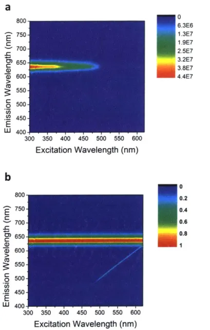
quantum yield and a suppression of the trap emission and 2) independent control of the shell thickness. This synthetic protocol resulted in nanorods that remained very ionodisperse at the batch level even as the shell thickness was continuously increased. In order to study the effective monodisperisty of the sample as it relates to the optical properties of the system, the ensemble and average single nanorod spectral correlations were measured using solution-Photon Correlation Fourier Spectroscopy (s-PCFS, see Fig. 2-5)9. From the small difference between the two spectral correlations, one can readily conclude that the inhomogeneous broadening of the sample only results in a minor contribution to the overall spectral width. In addition, the particles were highly uniform and crystalline at the individual nanorod level as can be seen from the high resolution TEM in Fig 2-6a and 2-6b. The uniformity achieved after the second growth step appears to be a, significant improvement from the initial nanorods, where the fast injection frequently results in the appearance of visible kinks as well as other crystallographic defects such as edge dislocations (see Fig. 83).
1 Single Nanorod Ensemble J-, 0.5-0 -400 -300 -200 -100 0 100 200 300 400 Spectral Correlation (meV)
Figure 2-5: s-PCFS traces showing the ensemble and average single nanorod spectral correlation of sample
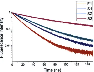
Table 1: Dinensions anid Fluorescence QuaiLntuin Efficiency of Nanorod Samples
Sample Length Width Fluorescence Quantum Yield
(%)
(nm) (nm) Lifetime (ns) F1 44 4 5.5+0.2 14 59 + 1 S1 ,453 6.3 +0.2 23 95 1 1 S2 4213 7.0+0.2 29 98 2 S3 103 9.5] 0.2 6( 85 1 1In order to systematically sty J h Ow evolution of the electron ic and optical
properties of
the
new nanorods, a size series was prepared by firstcreating
a batclh of nanorods using the conventional fast-injection based growth (denotedp1)2, wih1ich was then subjected to an additional slow growth steps to create two new samniples, which we denoted in the order of increasing thickness
as
S, S2. finally
in order to even iore (rasticallv increasethe
shell thickness, sample S1was sibjected to one additional slow growth, Yielding the sailple denoted S3. As
can be seen Irom table 1, while the length of all the four saiples is al]most iunchanged (ranging from 40nni to 45nn) as additional growth along the axial direction was balanced by the general tendency of the particles to becomiie mn ore spherical after prolonged reaction times. In contrast,
the
tih ickness increased continuiotisly from 5.5ni for [1 to 6.3, 7.0, and 9.5 in S1, S2, and S3respectively. BY taking into account, the initial size of the core (d--.9nmiii) and
the
thickness of each individual CdS layer, we can estimate thechange
in thethickness of
0.35nm)
to be from 1 in F1 to 2, 3, and 7 respectively in S1,S2,
andS3.
One key advantage of dividing the shell growth in two steps is to allow for an independent control of the length and thickness of the nanorods, allowing for the synthesis of uniform particles with a wide range of aspect ratios for any particular length. While conventional fast growth techniques yield highly uniform particles with a tunable length, changing the thickness has proven to be much more challenging since varying most synthetic parameters such as the amount of precursors injected and the reaction time predominantly affects the length while leaving the thickness largely unchanged.20, 21 While some progress has been reported for preparing thicker shelled nanorods by using a higher injection temperature, this approach nevertheless still resulted in coupled growth of the nanorods along both their long and short axes.28 In contrast, using our method, the first step results predominantly in growth along the long axis, while the second step occurs under conditions that promote symmetric growth in all directions Therefore, by carefully selecting the reaction conditions our method allows for core/shell nanorods with a desired combination of length and thickness. As a final note, because the shell is in equilibrium with the reaction precursors, under conditions that promote isotropic growth particles tend to become rounder. As a result, during the second step, the length may remain constant or even decrease even as the volume is increasing. This fact should be taken into account when designing the growth of the shell in order to obtain the target dimensions.
*< ,\ A t -4 -~Nb Lf~ $
/
I~ I 'I N.' / '1 ;t 9~.-~41450nm
* V:-.6 , -,~
I d10nm
Figure 2-6: TEM rmicrograph of the an0orods after the slow-shell
growth: a) a miCrograph of sample S] d ) High Resolution TEM