A Circular Pipelined Bus Architecture
for High-Speed Computation
by
Patrick R. Antaki
It
Submitted to the Department of
Electrical Engineering and Computer Science
in partial fulfillment of the requirements
for the degree of
Bachelor of Science in Electrical Engineering
at the
Massachusetts Institute of Technology
June 1984
Copyright (C) Massachusetts Institutp of Technology 1984
Signature Redacted
Signature of Author .... ...
Department of Electrical Engineering and Computer Science
Signature
Redactedm"l's
Certwifedby ... ... . ...Thesis Advisor: Stephen A. Ward
Signature Redacted
A ccepted by ... -- -- - -- - -- - --.-- -- - -- -.-- --- ---- -Chairman, Departmental Committee on Theses
MASSACHUSETTS INSTITUTE
OF TECHNOLOGY
JUN 2 11984
I
Miribraries
77 Massachusetts Avenue
Cambridge, MA 02139 http://Iibraries.mit.edu/ask
DISCLAIMER NOTICE
Due to the condition of the original material, there are unavoidable
flaws in this reproduction. We have made every effort possible to
provide you with the best copy available.
Thank you.
Some pages in the original document contain text
that runs off the edge of the page.
A Circular Pipelined Bus Architecture
for High-Speed Computation
by
Patrick R. Antaki
Submitted to the
Department of Electrical Engineering and Computer Science
on May 18, 1984 in partial fulfillment of the requirements
for the Degree of Bachelor of Science in Electrical Engineering
Abstract
A new architecture for high-speed computation has been conceived and partially implemented. The
architecture features a number of innovations in the field of parallel processing of a single or multiple
tasks at the low level of computation. It also provides tremendous hardware and software flexibility in
terms of optimization and implementation of programs. The result is a TIL computer that can attain
the performance of a CRAY-1 at a small fraction of the cost.
Thesis Advisor: Stephen A. Ward
Table of
Contents
Chapter One: Introduction 7
1.1 The Problem: Today's Computers 8
1.2 Some proposed solutions 9
1.3 The Influence of Technology 10
Chapter Two: The GAMMA Concept 11
2.1 The Bus 11
2.2 The Modules 13
2.2.1 Arithmetic/Logical Modules 13
2.2.2 Memory Modules 19
2.2.3 Program Sequencer Modules 22
2.2.4 Other Modules 23
2.2.5 Bus Saturation Logic 24
2.2.6 Global Clocking Issues 25
2.3 On the issue of data-dependent program flow and branching 26
2.4 Towards the Implementation of a Real System 28
Chapter Three: Theoretical Performance 29
Chapter Four: The Hardware Implemented 36
4.1 The Bus and Backplane 36
4.2 The Add Module 37
4.3 The Multiply Modules 39
4.4 The Program Sequencer Modules 40
4.5 Bus Saturation Logic 40
4.6 Clocking Methodology 41
4.7 Nu Machine Interface 42
4.8 Results 42
Chapter Five: The Future of the GAMMA Concept 43
Appendix A: Backplane pin-out assignment 45
Appendix B: The Adder Module 47
Appendix C: The Multiply Module 51
Appendix E: The Bus Saturation Logic 58
Appendix F: The Clocking Circuitry 59
Table of Figures
Figure 2-1: The Bus and the Modules
12
Figure 2-2: Address Re-allocation example in Hardware
15
Figure 2-3: Possible Data Path for An Arithmetic Module
17
Figure 2-4: Program: n successive operations
18
Figure 2-5: Arithmetic/logical module programming model
18
Figure 2-6: A floating-point addition programming model
19
Figure 2-7: Possible Data Path for an Associative Memory Module
20
Figure 2-8: Slow Memory Programming Model
21
Figure 2-9: Faster memory programming model
21
Figure 2-10: A Limited Implementation of a Sequencer Module
22
Figure 2-11: The Bypass Switching Module
27
Figure 3-1: Control-Flow Graph for the Test Program
31
Figure 3-2: Actual Sequencer Output for Test Program
32
Chapter One
Introduction
This thesis concerns itself with the problem of high-speed computation. I have proposed a new
architecture for computation which is highly parallel and features a simple programming model. The
motivation for this research is two-sided: the shortcoming of today's computers in terms of the
speed/cost performance, and the somewhat recent shift of the engineering community from hard
experimentation to computer simulation of various systems that has created some very
computationally intensive needs for numerical computing power.
The applications that I-speak of range generally in the following domains:
* Number crunching: typically these numerical programs solve PDE-type equations, or
matrices of non-linear simultaneous equations. This type of application has simple data
structures (arrays or matrices) that are one-level deep. The programs are simple
FOR- NEXT loops. This is an ideal application for the GAMMA architecture.
* Artificial intelligence: this field is characterized by the use of multiple-level data
structures, and is in need of an advanced program development tool. This application is
not easily implemented on a GAMMA computer.
* Concurrent Real-time Computing: this is typically used for process control in factories or
power-plants. In this domain, the function or program is pre-defined, and the system is
almost always running the application, processing asynchronous inputs and computing
outputs. The GAMMA architecture can deal with asynchronous inputs, but the actual
time till completion of a task, although generaly fast, is not easily predictable.
Today's general-purpose computers are not efficient in these applications, and the
supercomputers are too expensive. My proposal is the first step towards a compromise of these two
shortcomings.
1.1 The
Problem:
Today's Computers
Today's
computers,based
on the Von-Newmann model of computation have been very succcssful in the general-purpose, multiple-user environment. The general architecture corresponds to an S1SD model, consisting of a main system bus, a CPU, some form of primary storage and some secondary storage. The issues in determining the performance such a common-bus architecture aretypically the following: " Bus bandwidth
" Processor execution rate
" Instruction complexity
" Main memory speed
" Main memory size
" Memory hierarchy organization
Each of these aspects has been optimized to perform to its fullest by using a number of clever architectural tricks. The processor section for example, has been pipelined and has become more intelligent (i.e. it can understand and execute more complex instructions, through the use of microcode); a cache system has been invented and has sped-up the effective memory bandwidth (cache hit ratios of 90% or greater are not uncommon); memory itself has been interleaved and organized in many fashions to achieve greater bandwidth (an extreme case is the CRAY-1 whose main memory is interleaved 64 ways). Some implementations have widened the bus and memory to increase the throughput. All of the previous solutions do not offer a significant potential for increasing the processing power of a computer by orders of magnitude to meet the demands of today's applications.
It is quite clear that today's general-purpose computer architectures are limited from great enhancements in performance by the nature of the memory and the bus. The bus bandwidth is limited by physical interconnection constraints, such as signal transit time (typically through a few feet of backplane wire) and excessive capacitive and resistive loading on that bus.
1.2
Some
proposed
solutions
It is important to point out that aside from performance and price, other issues are also crucial.
In particular, a computer system should provide the programmer with a model that does bring out
the number of processors involved, the vagaries of interconnection strategies or other hardware
subtleties. Second, in spite of the Law of Diminishing Returns, the architecture should increase its
performance as linearly as possible with the increase in the number of processors in the whole system.There have been a number of proposed solutions attacking the problems I have just mentioned.
Some have been implemented in successful computers, others are still in the definition stages.
The basic computer today is of the SISD type, and it has already been pointed out that the
performance limit on this model is closing too fast. Other models such as the SIMD and the MISD
exist. It is generally agreed that these two types are not very useful for implementation as general
purpose machines, and indeed very few applications have requirements that would fit the MISD and
the SIMD computational models well.
Today almost all research efforts in the computer architecture field are geared towards
concurrent computing. The simplest and most explored area is in the interconnection of a large
number of self contained processors (they may be of any size) with a high-speed link among them. so
as to be able to communicate in real-time and execute parts of a large program concurrently. This
scheme must not be confused with the older idea of interconnecting large computers through a
low-speed link to batch jobs at different locations according to load variations. In the multiprocessor
world, we can imagine a number of processors running parts of a large program, sharing memory,
and communicating through variables in that memory. The main problem with that approach is that
of extracting all of the concurrency from a task and subsequent assignment of these tasks to each
processor. Another problem is that of variable passing among program modules, and thus among
processors. The issue is to communicate properly among modules (with all of the interlocking
protocols to insure synchronization) without too much overhead.
This approach to increase the performance of computers today is the easiest and the obvious
next step. Nevertheless. it is not necessarily true that performance for many applications is truly
enhanced by this solution. A number of people agree (as well as myself) that a totally new approach
to the computing model of the world is needed. That new approach can be coined the term data-flow
research. The GAMMA architecture is a data-flow program execution machine. One can write
programs for the G ANM M A urchitccturc as a llow-graph (mole on that later).
The reader is encouraged to look through the references at the end of the thesis for some
extremely useful papers on the discussion above. It is not worthwhile to argue the above point
further, because there are still at this moment no clear-cut answers which point in either direction.
1.3 The Influence of Technology
One very important aspect which affects computers' performance is of course, the underlying technology, or the hardware. Almost all of the tricks and quirks invented in today's computers can be related to the particular technology's shortcoming in either switching speed or gate density. Indeed today's technology is not fast enough to satisfy our computational needs using today's architectures. The whole architecture game is a way to get around the fact that signals require time to propagate and that circuits need time to compute. These fundamental facts must be kept in perspective when designing a machine, since they are the ultimate criterion in the making of almost all of the architectural decisions in the design process.
Today there are a number of technologies available to the computer designer, each with its strong points and weak points. The fastest (and most expensive in terms of silicon costs, power dissipation, gate density, difficulty of design, etc.) is Emitter-Coupled Logic, or ECL. The CRAY computers are built out of ECL, which is the primary reason why they run with a 12.5 nanosecond clock cycle, as opposed to a typical 200 nanoseconds for other computers not using ECL. Another technology, TFL, is the most popular because of the speed, power, ease-of-use and integration trade-offs it offers. MOS technology is the only viable technology for large memory systems and VLSI chips. We will not consider this technology due to the nature of the proposed architecture (more on that later).
Chapter Two
The GAMMA Concept
'T7he GAMMA architecture is my proposal to attempt to solve the problems cited earlier in this
thesis. It is best introduced by an analogy.Imagine an assembly line belt that is circular (like the airport baggage pick-up belts) which always runs in one direction. 'here are 100 people gathered all around the belt, each of whom can perform a single specific task. On this belt someone places objects along with a little note containing the name of the recipient further down the line, and some instructions. As the parts go down the belt, each person has to wait for an object with his/her name on it so that they may pick up that part and begin working on it as per the enclosed instructions. When that person is done with their task, he/she will return this part onto the line as soon as there is an opening on the belt and then wait for a new one assigned to him/her.
The concept is simple. If we replace the people with computational modules. and we replace the belt with a circular pipeline, we have a method of communicating information, or instructions to each module through this common pipelined link, called the bus. So that at each pipe stage exists a module which looks at the bus every clock cycle, and determines whether that data token is addressed for it. If it is, then the module "lifts" this token from the bus, and creates a "free" spot. The whole pipeline is clocked synchronously, and data moves around the bus in a circular fashion, every clock cycle moving by one pipe stage.
2.1 The Bus
The bus consists of three of fields: address, data and control. The address field is used to tag the data so that each module can compare the contents of the address bus against a pre-assigned address (called the op-code) in order to decide whether the data token is destined to it or not. The control field contains the following signals:
* VALID, which is used to determine whether each particular token corresponds to valid
information:
if VA 1.11)
isde-asserted then that
pipe stage is free, or empty."
R FSI.T. which is a system-wide reset.
" WAIT. which prevents a module from sending data onto the bus (c\cn though the bus
might have empty slots).
" INFO. a set of bits used for "special instructions", this can be be regarded as an extension
to the data bus. for general-purpose
use.
MOD.1 MOD. 2 oD. 3
ipe Stage
MD.98
4BUSMOD. 4
Pipe Stage Pipe Stage
mm.7 Dm.6 MD.5
Figure 2-1:The Bus and the Modules
The whole idea behind this bus is that the wire length and loading are extremely limited (on the
order of a few inches and a small fan-in), and thus the speed of the bus pipeline is quite high. At
every clock cycle all that need be done is an "equals" compare and a latching of data (picking up data
-from the bus). If a module Wishes to communicate with another module, it waits for an empty slot on
the bus and puts its token on the bus (by placing the data, address, control bits as it needs to, and
then asserting the VALID signal). A number of clock cycles later, equal to the number of pipe stages
that the recipient module is away from the sender module down the pipe (a number equal to or
greitcr than one, in the case where the recipient is adjacent to the sender "downstream", but less than the number of stages on the bus, in the case where the recipient is adjacent to the sender, but this time is "upstream" from it), the recipient receives the data on the bus, and captures it. Note that we have placed no restrictions on the nature of the information that the data bus contains. Its context (be it an operand, a control field for the recipient module, a number to be stored, an address, a byte from a terminal, etc.
)
is strictly contained within the sender/receiver relationship.2.2 The Modules
'[he modules consist of a bus interface section, which must run as fast as the bus clock speed, and a functional part, which performs the actual function of the module. In one clock cycle, the module must perform a comparison of the address bus with its pre-assigned address to detennine if that data token is addressed for it. In the case of a match, the data and control busses are latched internally to the module and the VALID bit is de-asserted. Now some other module down the line can use this newly-created empty slot on the bus to transmit its information to some other module it is in process of "working" with.
The functional part is the module's guts, and it consists of any one of a number of possible operations that the module might perform. These are generally speaking arithmetic/logical, storage, I/O, program sequencers, etc.
2.2.1 Arithmetic/Logical Modules
This type of module performs operations such as floating-point arithmetic, and some logical functions. The general procedure that this module undergoes is the following:
" Reset, at which point the module sits in an idle state, looking at the address bus every clock cycle, and comparing the address bus to its pre-assigned address, which is its op- code.
" Upon a match on the address bus, the module picks up the data, and replaces its original compare address with the new one that came on part of the data bus. The reason for this "extra step" will become clear soon.
" Now the module compares the address bus against its New Address (NA), and waits for a match.
1
A
IIach
occurs, and the data is picked up again. This Lime, that new token is actually an operand. This is either the A or B operand, depending on the state of the INFO bits. Note that the order of the operands' arrival is immaterial.* The module waits for the second operand to arrive in the same fashion as the first (under the same New Address).
" Now the module begins its computation.
" While the module is computing, the bus is still going at full speed, but now that operation is being performed asynchronously to the bus. During this time, the module does not look at the bus, as it is busy computing. The computation time is arbitrarily greater than the bus period.
" Some number of clock cycles later, the computation is finished, and the module now waits for an open slot on the bus (by looking at the VALID signal).
" When it sees the open slot, it puts the result on the data bus. The address bus will be loaded with the address of another module to which that newly-computed token should go. This value (the Result Address, or (C> ) was transferred to the module during the same transfer of the New Address (the New Address and the Result Address are both sent on the same token on the data bus. Since in this conceptual case the data bus is 32 bits wide, and the address bus only 16, we can send two address values on the data bus simultaneously.
* Now that the module has completed an operation and sent out the results it goes back to responding to the original address it had (the op-code), waiting for a new access to it.
A "typical" GAMMA computer would consist (for now) of one pipelined bus with over 100 stages. Let us assume that the whole computer consists of just 100 identical (and thus answering to the same op-code, call it Op-code-A) modules that just perform additions, and a single program sequencer. These adding modules accept two operands, A and B, as well as a New Address (NA) and a result address <C>. Then they perform the add operation on these two operands. When the operation has finished executing, these modules send out their result "A + B" to <C>.
The problem of programming such a machine is fairly complex. since in order to perform an operation, one must know at every time which module is busy performing an operation, and which one is not; this way one can send operations to the free modules in order to optimize use of the
DATA BUS DATA
IATCH
TO NEXT PIPE STAGE
ADDRESS ADDRESS BUS
IATCH
NEW
ADDRESS ADDRESS ADDRESS
IATCH M COMPARATOR ,ATHOUTPUT - ("This Tokeni > is for us!") HARD-WIRED OP-CODE SELECT OLD OR NEW ADDRESS
Figure 2-2:Addrcss Re-allocation example in Hardware
modules in time. This is a very complex task and it requires that the programmer know a number of low-level details about the hardware such as: length of the pipe (number of stages), speed and location on the pipe of every module, etc. The solution to this programming problem is simple if we perform Dynamic Address Re-allocation of each module as described in the previous steps. If we have 100 identical modules waiting for an operation request, then we really don't care as to which module performs the operation, rather we just want it to be performed and the result sent to the appropriate recipient module. Thus, the solution is to let all of these identical modules respond to the same address when they reset, that is, their op-code. Then the module which happens to first see an operation will capture if, and will then respond only to the New Address NA (that came on the same first token) by re-assinging its compare address to this New Address. The purpose of that is to be able to split up the computational model into atomic operations (such as operation number one is 4+7, operation number two is 3*2, etc.) as opposed to computational units (module number one is
Address number one, module number two is Address two, etc.): the hatter irc hardware units, and much more difficult to keep track of. Atomic operations involve the transfer of group of tokens to a single recipient, but from an arbitrary number of senders (for the same atomic operation).
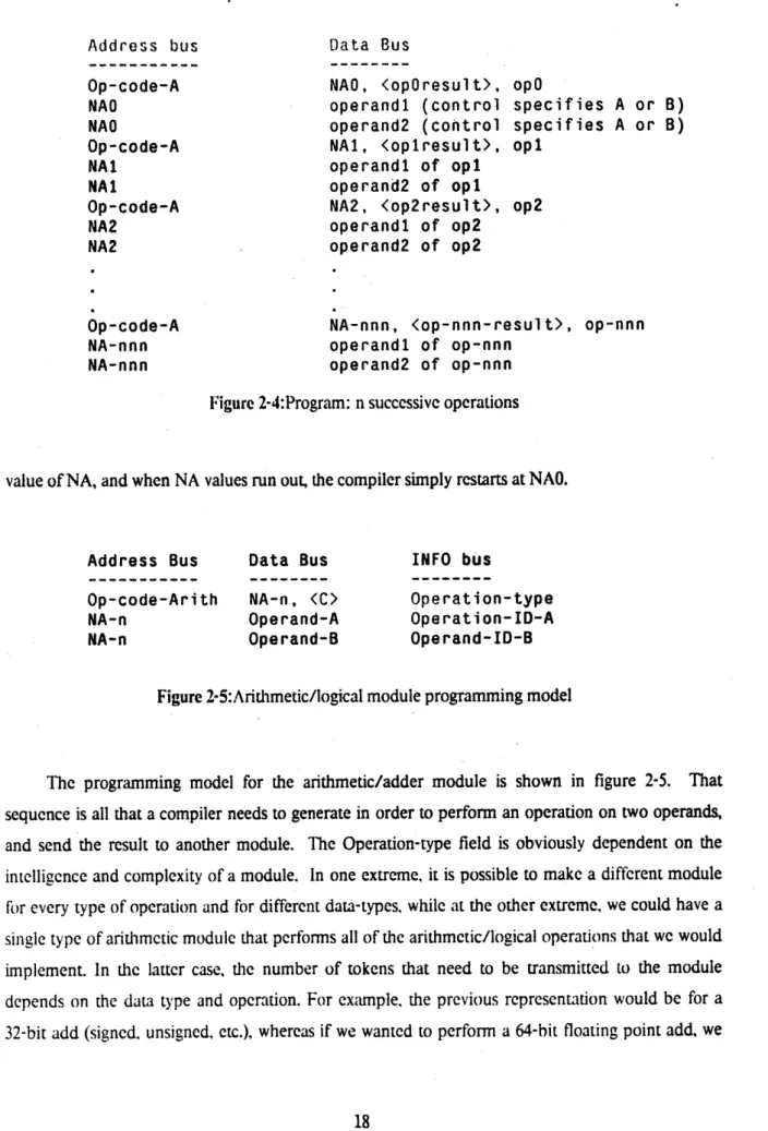
Now if we have a large number of independent operations to perform, we would execute the "program" in figure 2-4.
Note now that opO, opI, etc. are bits in the INFO field which specify which type of operation to perform, such as an add, multiply, logical AND; thus our module now is obviously more intelligent.
What happens in the above example is that each module whose pre-assigned address is Op- code-A will respond to that address when it comes on the bus, and it will subsequently perform the atomic operation op-nnn. So the first adder downstream from the program sequencer will capture the first operation opO, then the second adder module will capture opl, etc. There is no problem of different modules capturing operands of another's, since the atomic representations NA-n are all unique. The assignment of atomic operations to modules will occur automatically because of the Dynamic Address Re-allocation scheme, so as to maximize the use of all the modules that respond to op-code-A.
There are a number of details to point out. First, the order of arrival of the first and second operands is immaterial. Second, the program has no way of knowing which module captured which operation. Third, the program does not know how fast the modules perform their operations (each module need not be as fast as another "identical" module of op-code-A). Third, the program does not have to know how many modules of type op-code-A are on the pipelined bus. Fourth, the program will always execute properly (but not necessarily as fast) as long as there is at least one module that performs op-code-A. Fifth, the values NA-n are generated arbitrarily to uniquely identify atomic operations; thus if there are n modules, and presuming that they are all of the same speed, the number of unique NA values that we have to create is n. This is not a limiting factor in the performance, as realistically if there are 250 modules in the whole system, then we would perhaps need an address bus as wide as 10 bits: adding one more bit to the address bus would make the assignment of NA values even easier while not affecting system performance. and affecting cost only marginally.
These NA values are generated at compile time, and the easiest way to generate them is to have a counter that goes from some NAO to NA-n, and assign each operation as it is compiled the next
CLOCK DATA IATCH ADDRESS IATCH Cr -II W INHIBIT W. -I 4-) 0 0.
1
fDArD TA BU TO NEXT PIPE STAE A JDRESS BUI L _________________________________ 0 __T__ L BU ONT1OL ATCH BUS LDA LT. B LT. LDB Operation circuit CONTROL CIRCUIT LDA0 LDB LD(C) CMWTILBUS CLOCK LD (C)_T
AB NA LT. >() LT (C) out ADDRESS DECODER LD (C) OP CODE -- TE LD/NEWADDRESS - INHIBIT PRESET D -L/NEWADDRESSAddress bus Op-code-A NAO NAO Op-code-A NA-1 NA1 Op-code-A NA2 NA2 Op-code-A NA-nnn NA-nnn Data Bus NAO, (opOresult>, operandi (control operand2 (control NA1, (opiresult>, operandi of opi operand2 of opi NA2, <op2result>, operandi of op2 operand2 of op2 opO specifies A or B) specifies A or B) opi op2
NA-nnn, <op-nnn-result>, op-nnn
operandi of op-nnn operand2 of op-nnn
Figure 2-4:Program: n successive operations
value of NA, and when NA values run out, the compiler simply restarts at NAO.
Address Bus Op-code-Arith NA-n NA-n Data Bus NA-n, <C> Operand-A Operand-B INFO bus Operation-type Operation-ID-A Operand-ID-B
Figure 2-5:Arithmetic/logical module programming model
The programming model for the arithmetic/adder module is shown in figure 2-5. That sequence is all that a compiler needs to generate in order to perform an operation on two operands, and send the result to another module. The Operation-type field is obviously dependent on the intelligence and complexity of a module. In one extreme, it is possible to make a different module for every type of operation and for different data-types, while at the other extreme, we could have a single type of arithmetic module that performs all of the arithmetic/logical operations that we would implement. In the latter case, the number of tokens that need to be transmitted to the module depends on the data type and operation. For example, the previous representation would be for a 32-bit add (signed. unsigned, etc.), whereas if we wanted to perform a 64-bit floating point add, we
vould
do
the
sequence shown in figure 2-6.
Address bus Data bus INFO bus
Op-code-Arith NA-n, <C> Operation-ID-64bit-float-add
NA-n Operand-a Operand-A-lower-half
NA-n Operand-A Operand-A-upper-half
NA-n Operand-b Operand-B-lower-half
NA-n Operand-B Operand-B-upper-half
Figure 2-6:A floating-point addition programming model
Note that again the order of receiving of the 4 data tokens is not important, but the operation may not begin until all 4 have arrived (there might be room for optimization here, if for example the exponent parts of A and B are sent first, then the module could perhaps start processing the exponent operation before the mantissa). Note also that the result of the above operation is a two-token quantity, and that a protocol for the module to transmit its result to <C> exists, such as presetting the INFO bus to correctly identify which part of the result is being sent. These are all implementation details.
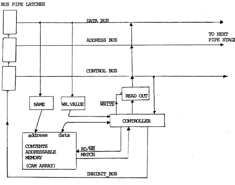
2.2.2 Memory Modules
These modules are temporary storage modules, which are used to store partial results, variables, etc. The memory model for the GAMMA machine is that of a tagged-memory system. That is, if a variable needs to be stored, the name and data must be kept together.
A memory module consists of a bus interface part and a simple associative memory part. When a program sequencer needs to store a value, it would send the module (which is responding to its "op-code") a New Address, and then under the NA it would send the NAME of the variable, and in another token the VALUE of the variable. Then the memory module, upon completion of storage would go back to its reset state looking for more STORE or READ op-codes.
In the case of a READ, the program sequencer would send a read op-code along with an NA and a bus address to which to send the VALUE of the variable, and on a subsequent token send the NAME of the variable under the bus address NA. Basically, we have atomized the READ and
BUS PIPE ' 1 BUS& ADDRESS BUS TO NEXT PIPE STAGE
1
A
CONTROL BUSREAD OUT
'WR. VALUE WRIT1 CONTR0LLERI4
INHIBIT BUSFigure 2-7:Possible Data Path for an Associative Memory Module
WRITE operations as well.
If we follow through the progress of these operations on a "typical" GAMMA system which
would have a number of memory modules (again each identical like the arithmetic modules), we
come to the conclusion that the effective memory READ times are terribly long. If we send out a
WRITE operation, we have no knowledge as to which memory module actually has the variable
stored, just as in the arithmetic case where we didn't know which module performed the operation.
Now when a READ comes along, the first memory module that intercepts this operation will
pick-off that command off the bus, and begin a search through its whole memory. If the variable is
found. then the value is sent ofT to the appropriate module, if on the other hand the scarch fails, then
the memory module must rcturn the two-token operation onto the bus to let other mcmory modules
NAME
address
data
ADDRESSABLE
(M RRY
(CAM ARRAY)
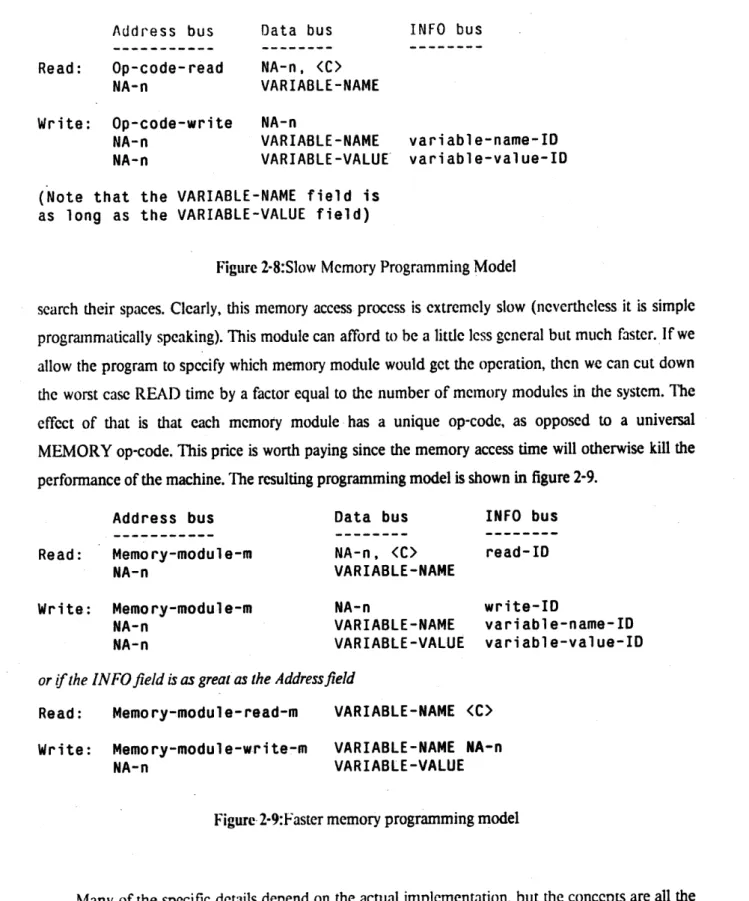
AD/MAN IA'ICHESAddress bus Read: Op-code-read NA-n Write: Op-code-write NA-n NA-n Data bus NA-n, (C> VARIABLE-NAME INFO bus NA-n VARIABLE-NAME variable-name-ID VARIABLE-VALUE variable-value-ID (Note that the VARIABLE-NAME field is
as long as the VARIABLE-VALUE field)
Figure 2-8:Slow Memory Programming Model
search their spaces. Clearly, this memory access process is extremely slow (nevertheless it is simple programmatically speaking). This module can afford to be a little less general but much faster. If we allow the program to specify which memory module would get the operation, then we can cut down the worst case READ time by a factor equal to the number of memory modules in the system. The effect of that is that each memory module has a unique op-code, as opposed to a universal MEMORY op-code. This price is worth paying since the memory access time will otherwise kill the performance of the machine. The resulting programming model is shown in figure 2-9.
Address bus Read: Memory-module-m NA-n Write: Memory-module-m NA-n NA-n Data bus NA-n,
<C>
VARIABLE-NAME NA-n VARIABLE-NAME VARIABLE-VALUE INFO bus read-ID write-ID variable-name-ID variable-value-IDor if the INFO field is as great as the Address field
Read: Memory-module-read-M VARIABLE-NAME (C>
Write: Memory-module-write-m VARIABLE-NAME NA-n
NA-n VARIABLE-VALUE
Figure 2-9:Faster memory programming model
Many of the specific details depend on the actual implementation, but the concepts are all the same. The storage of temporary information on the GAMMA bus through the use of memory modules is inefficient in that both variable name and value must be stored. I can conceive of certain
modules that
would store blocks of information.cach
block sharing a single name: this is just One of many possible implementationswhich again
woulddepend on the actual
requirementsand other
design issues of a real system.2.2.3 Program Sequencer Modules
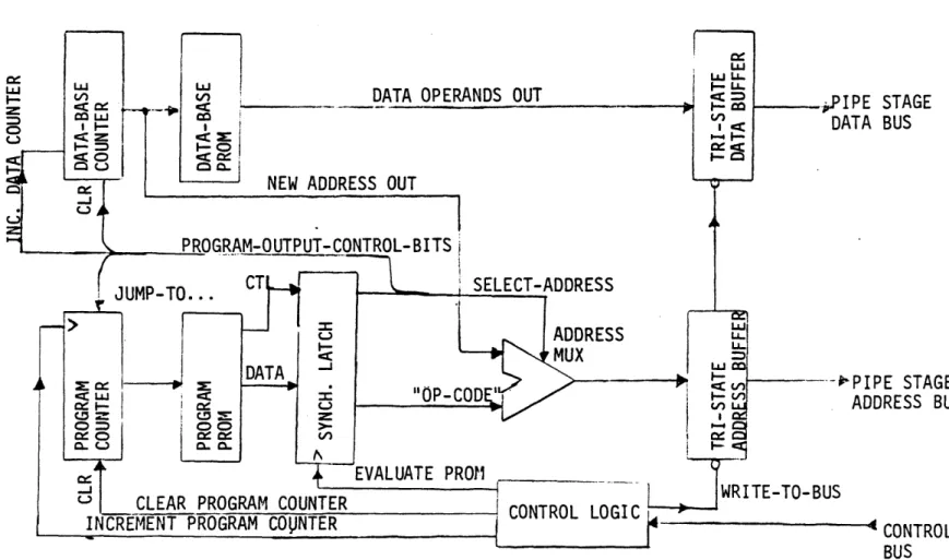
The program sequencer modules are the ones to output the tokens that initiate and synchronize the operations on the GANIMA bus. Such a module contains the actual compiled program. and would be likely to contain data as well. However it is possible for a separate module (such as a memory module or an
I/O
module) to provide the data according to commands of the program sequencer.)
_DATAOPERANDS OUT
PIPESTAGE
CD
I -
DATA BUS
NEW ADDRESS OUT
_
1
PROGRAM-OUTPUT-CONTROL-BITS,
U -.
CT
1
_ SELECT-ADDRESS
ADDRESS
DATA
101
R
-- .,---PIPE
STAGE
ADDRESS BUS
EVALUATE PROM
-a
WRITE-TO-BUS
CLEAR PROGRAM COUNTER
CONTROL LOGIC
INCREMENT PROGRAM COVJNTER
'CONTROL
BUS
Although the only job of this mohdLuIC is LO SCnd out sCquerntially thc contets of a buffer onto
the bus at as fast a rate as possible, it might entail so more intelligence. In particular, if this module
consists of a microcoded machine, it could perhaps implement some simple loops and branches. The extent to which this intelligence affects the overall performance is discussed in section 2-3.A typical program sequencer module would be the most complicated module in the whole system, in terms of design, data path and control. Such a module is one of the places that a link to a host computer might exist, or at least this is where the compiled code (arriving from whatever source of generation) is "executed".
There can be an arbitrary number of these modules per system. This effectively means that numerous programs can be running at the same time, sharing the same hardware (bus and modules). The only requirement for running numerous program sequencer modules simultaneously is that all of the New Addresses generated for identifying operations be unique for each sequencer (unless some user wishes to play games with the timing of the system). These numbers are generated at compile time and can easily be controlled. The programs executing on each sequencer module can be totally independent, or can be parts of a larger program. If any sequencers use variables for temporary storage it is also important that the Variable Names from sequencer to sequencer be also unique.
Note that by the use of unique NA values, the architecture guarantees that accidental no inter-sequencer "cross-talk" will occur. The impact of this is important, because now it is possible to run totally separate programs simultaneously, without having to know anything about the other program's use of the same computational and storage resources that all programs are sharing. This is one aspect of abstraction on the GAMMA architecture that is very powerful.
2.2.4 Other Modules
A number of other modules are very conceivable. All sorts of computational modules can be designed into the GAMMA bus. These can be built out of combinational circuits, or can contain tiny processors that per'orm more complex algorithms on the data, or any other flavor of a calculating circuit. Other modules can be direct peripheral links for terminals, voice digitizers, video memories, digital-to-analog outputs for control, etc. Memory modules of all kinds can be built, each with its own programming model and its special features.
It is
an interrcsting point that a GAMMAmachine
might be easily optimized in hardware for the kind of application it is likely to run. For example, highly computational programs require more computational modules. Data switching applications would require more 1/O modules (here theGAMMA bus is used to read from one module input and write to another module output under
programmatic control, influenced perhaps by another.module input. This is one way to implement a
large, intelligent crossbar switch). VLSI applications could use a GAMMA machine where a large number of modules are DRC accelerator chips, each with its own memory and output (there is at least one DRC chip in existence, and this architecture is a good environment for such application- specific hardware).2.2.5 Bus Saturation Logic
One item not mentioned so far, but is the only piece of hardware in the GAMMA machine that does not actively perfonn useful work towards the accomplishment of a programmatic task is the Bus Saturation Logic. The purpose of this hardware is to prevent possible saturation of the bus so that no more communication can take place, in the case of a deadlock situation.
Here is how the deadlock can happen. If a program sequencer sends out tokens on the bus too fast, then all of the address modules will pick up their tokens and empty out that slot of the bus, and become busy for a while. Meanwhile the sequencer is still sending out requests onto the bus, and all of the addressed modules are now busy, thus unable to clear out any more tokens off the bus. But when these modules are done computing. they cannot send out their results back onto the bus because there are no more free slots (by then the sequencer will also be waiting for an open slot to dump out even more requests), and thus they cannot pick-up any new requests off the bus freeing some space. This is the deadlock. The only solution is a hardware "busy-gauge" on the bus which detects when the bus becomes too congested, and issues a WAIT signal to the program sequencer modules, which hold up their dumping out tokens onto the bus, until the bus "load" drops to a certain level.
Thus this unit has to effectively perform a large number of 1-bit additions (all the VALID bits at every pipe stage) every clock cycle: if the resulting number is greater than some value (which must be conservative. as the next clock cycle it is entirely possible that all modules are done computing and will dump out their results then, creating the deadlock at the next clock cycle), then WAIT is asserted. It would probably be a good strategy to keep WAIT asserted for a longer period than after the "load"
drops lower than the initial thrschold (a hystercsis etect). The actual number to use for a threshold
depends on the actual implcmentation. Nevertheless I have not conic up with any guidelines for
computing that number other than to be conservative while still allowing maximum use of the bus.
Perhaps one module that could be useful is a "temporary bus garbage collector". This module would
detect the condition where WAIT was asserted for some long period- of time, arriving at the
conclusion that a bus deadlock occurred, and then picking-up token off the bus, storing them away.
Later after the deadlock is resolved, it would replace these tokens in the order picked-up (although
the order according to the programming model is immaterial).
It is likely that performing n parallel 1-bit additions is awkward for almost any reasonably sized
GAMMA machine. Another approach that is almost as effective is to divide the bus into smaller
sections and perform the load check more times around the bus, by using more than one bus
saturation module, each working on a smaller number of pipe stages. Now there would be a number
of different WAIT signals, each corresponding to a smaller portion of the whole bus, and acting only
on that portion. It is still unclear as to whether this technique works for a machine with a small
number of closely clustered program sequencers. But some variation of this multiple level WAIT
generation could certainly simplify the bus saturation prevention
task.
2.2.6 Global Clocking Issues
In
an actual implementation of a large GAMMA machine, the clock distribution problem
could
become very important. All of the modules use the same clock, and clock skew must be extremely
small, corresponding to that allowed by the bus latches, on the order of 1 to
5
nanoseconds typically.
If the clocks are not all matched then the bus will not guarantee the integrity of its token transfer, and
the result is similar to a real-time bus error on any computer: unpredictable and potentially
catastrophic. The idea of adding some sort of error-detection to the bus is perhaps possible. To have
each module check the parity of the bus at every clock cycle would be very expensive and could slow
down the clocking rate. A better solution is to have a number of Parity Checker Modules scattered
equidistantly throughout the bus. The modules' only job would be to check the integrity of the token
at every clock cycle, and signal some global signal (not sent through the pipelined bus, obviously) that
an error occurred. The module would only check of course the tokens that have their VALID bit set.
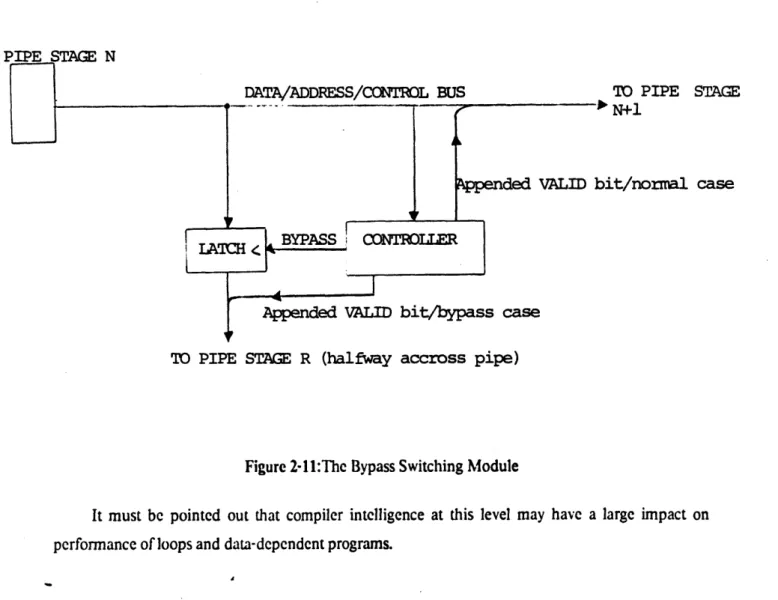
2.3 On the issue of data-dependent program flow and branching
In order to do branching and data-dependent decisions, the program must send the
argument(s) in token form down the bus to a module that performs the test and returns a logical
value, according to the result of the test. The result then gets transported back down the pipe to the
sequencer, which then can decide what to do next. During all that time, the sequencer is idle, as it is
at a branch point in the program, and needs some results to proceed further. This process brings out
the issue of circular bus latency. Depending on the size of the bus, this time could be too great.
One solution is to use very few loops in the program, and there are applications like that.
Another solution is to perform the test within the sequencer module, and thus keep it localized at the
expense of a more complicated sequencer (which is already quite complex). In the case of a typical
numerically-intensive simulation program, a typical case is the FOR-NEXT loop, where the number
of loop iterations is equal to the size of a data array. Thus the actual test is performed not on data, but
on a programmatically generated loop counter variable. For a small number of levels of depth of
loops (loop within a loop
... )
this hardware implementation is reasonable and offers a substantial gain
in speed for such loops over the pipe-bus method. The feedback into the sequencer from the bus is
still important, since there would otherwise be no way to conditionally branch on computed data that
exists on the bus. This operation is slow as I just showed. Another possible trick to reduce the bus
latency for program feedback is to have modules that would bypass one-half of the bus for certain
tokens, and let other tokens go through the normal path down the bus. This module is really a switch
that sends data down in different paths (2 or more) depending on the data itself. The design of that
module would depend specifically on the particular placement of each module on the bus. This
module conceptually could speed up all the tokens by bypassing parts of the bus; however, since the
context of the data is self-contained, that module would have to know to which address this token is
going to, and the addresses of the hardware modules are changing all the time (New Address,
op-code, etc.). Thus it is likely that these modules would only switch the paths of a limited number of
types of tokens which might be marked by either the address of a sequencer module (which is static)
or by some bits in the control part of the bus.
If one wishes to be clever one can let the program execute further down one path of the
program (chosing the path either arbitrarily or by some compiler directive based on past statistics
and/or compiler intelligence) while the branching decision is still being made. Then when the test
result comes back, either the sequencer disallows the last number of operations done, or if the
guessed path was correct, it could continue. This is
a messy
optimization.because the sequencer must
have a way to clear Out completely thc effect of executing the wrong code. The possibility of having a token circulating in the pipe that no moduic picks up, or that a module starts on an operation but never gets the rest of its tokens exists. The "lost" module that started an operation but was never sent its subsequent operands is a lost resource, and a potential source for errors: when we restart the use of New Addresses NA, this module will pick up another operation's token that has the same NA, thus creating some strange errors. 'lierefore implementing this strategy mLust be done carefully, and willinvolve some more complexity at the sequencer level.
PIPE STAGE N
DATA/ADDRESS/CONTROL BUS
Appended VALID b
Apende d BYPASSb y CONTROLLER
Appended VALID bit/bypass case
TO PIPE STAGE N+l
Lt/normal case
TO PIPE STAGE R (halfway accross pipe)
Figure 2-1 1:The Bypass Switching Module
It must be pointed out that compiler intelligence at this level may have a large impact on performance of loops and data-dependent programs.
2.4 Towards the Implementation of a Real System
In
order
to implement a system based on the GAMMA architecture, as in the design of any
computer, the final application must dictate its requirements onto the system. If we have a good idea
of the types of programs that will be running on that computer, we can easily optimize the
performance, or shift the potential performance to one type of instruction from another. It is possible
to write an instruction set for a GAMMA machine, where it turns out that each instruction
corresponds to the placing of a particular module that performs that instruction on the bus.
If the application is a typical signal-processing one, then we wish to place as many arithmetic
modules as possible (then we worry about whether these are general purpose, or floating-point or
bitwise modules, and the relative number of these), and would probably place only one or two Bypass
Modules. A similar argument can be made for every kind of application. It is important that the
designer not optimize the machine exclusively towards only one application, and effectively eliminate
certain instructions from the machine (which is also easy to do). Optimization must not preclude
generality (even if the machine would run much slower on some applications, it is important that at
least it be able to run them).
Chapter Three
Theoretical Performance
In this chapter I shall define one possible implementation of a GAMMA computer, and then
calculate estimates of its perfonnance. These estimates are all analytical and make a number of
assumptions listed below. The only way to prove the validity of these calculations is through the useof a GAMMA software simulator which one can use to run a variety of programs on, and experiment
with the effects of varying certain system parameters. This type of simulator has not been implemented, and is in fact the next step in the realization of the GAMMA architecture as a full-fledged machine. The author feels that these calculations are reasonable and realistic with what technology is today available.Here is a machine description along with the assumptions:
1. The data bus is 32 bits wide, the address bus 16 bits, there is 1 VALID bit, 1 RESET bit, 8 INFO bits.
2. The basic bus clock rate is 20 nanoseconds.
3. There are 100 general floating-point modules, and each can perform a 64-bit floating- point operation (plus, minus, multiply or divide) in 1000 nanoseconds.
4. A total of five token transfers are needed for every floating-point operation to be initiated.
5. There are two independent program sequencers performing similar programs on an equal-size data base of numbers.
6. The basic routine running on all the numbers in the data-base is:
F =(A +( B *C
) )
/Fi i i I i-1
and
F=
(
A +( B *C) )
/ 10
0
0
0
7. Note that the previous program requires that the result F be sent to two separate modules, the memory for a STORE and the next program loop for a DIVIDE. This means that we have a way to specify to the dividing module two destination addresses, thus we assume that the hardware is also more complicated so that it can perform this function, and that for the divide operation, we need to send an extra token which is the second destination address.
8. The input data base (consisting of A, B and C values) is resident in the program sequencers.
9. There are two memory modules to which STORE operations are performed (one memory module per program sequencer). Each program sequencer will send its values of Fs to one of these two modules.
10. The program sequencers can send out data onto the bus at the basic bus clock rate of 50
MHz.
11. The array size of the input numbers data base is huge, 10000, so that initial bus latency is not a factor.
In the above description, a number of important features were left out, such as branching, data-dependent program flow, etc. These functions are all presumed to have been taken care of in the compiler, and have already been identified as sources of problems earlier. For this example we shall ignore these problems.
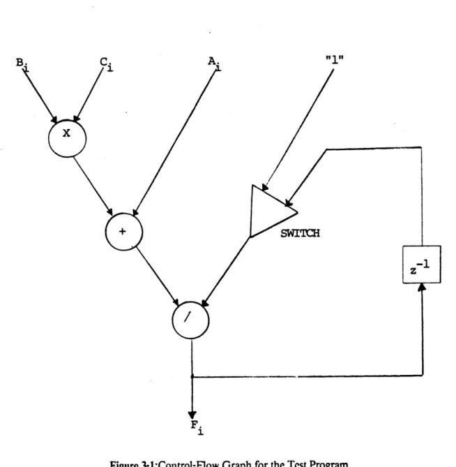
It is clear that there are two "languages" mixed together in the program of figure 3-2: bus operations, and internal loop-count operations (internal to the program sequencer). Note also how one operation will send its result to the next operation automatically, and that the first token of every operation is addressed to "Arith" which corresponds to any free arithmetic module. The program in figure 3-2 is the line-for-line symbolic equivalent of a typical GAMMA compiler output.
B. C. A. "1"
x
+ SWITCH
F.
:1
Figure 3-1:Control-Flow Graph for the Test Program
Let me also point out that the computation in figure 3-1 has, in spite of its appearances, only a minimal amount of parallelism. The reason is that even if one can perform the addition and jnultiplication parts of iteration n +1 before iteration n is done, this iteration will only complete after iteration n has completed, and so on. That is to say that the iteration may start earlier than in a non-parallel case, but cannot tenninate earlier than the non-parallel case. The effect here is similar to an adder carry chain, where the result must percolate through the whole length of the computational
structure, evcn though the inputs arc present and stabic for a long time. I3cause of
that, we will
simulate the performance of a slightly different program: this one will use
four
input numbers to
perform the multiplication, addition and division. That is to say that the divisor will not be the result
of the previous iteration, but a constant.
Address Bus Data Bus
BEGIN: STORE LOOP COUNTER
INFO bus B*C : Arith NA-n NA-n NA-n NA-n A+# : Arith NA-( n+1) NA-(n+1) NA-n, NA-(n+1) Bi-lower-half Bi-upper-half Ci-lower-half Ci-upper-half NA-(n+1), NA-(n+2) Ai-lower-half Ai-upper-half Mpy-64bit-float a-op-lower a-op-upper b-op-lower b-op-upper Add-64bit-float a-op-lower a-op-upper
the
second
operand
=
B*C will come directly from operation NA-n
#/F
Arith
NA-(n+2), NA-(n+4)
NA-(n+2)
NA-(n+3)
these two instructions are only needed for first iteration through
loop. All other times this operand will have come from operation
number NA-{n + 1+ 5*L] where L is the loop iteration counter value
NA-(n+2)
integer-i-lower
NA-(n+2)
integer-i-upper
this
instruction
preparesfor the output of the F value by
starting a WR I TE operation and sending
as
VA R I ABL E NA ME the
OUT:
OUTPUT
NA-(n+4)
NA-(n+4)
loop-counter-value
END-OF-LOOP-ITERATION:
INCREMENT LOOP COUNTER
Div-64bit-float second-result-address a-op-lower a-op-upper index write-operation variable-name
CHECK LOOP COUNTER END
BRANCH: FINISH (end)
B*C (continue)
Figure 3-2:Actual Sequencer Output for Test Program
Now to evaluate the performance of one program running only, we can say that:
Bus Latency = 100 stages * 20 nsec/stage = 2000 nsec = 2 modules' delayWe expect that the purC computational time will be:
Time
=
1000 nsec/comps * 10,000 iterations * 3 comps/iteration / 100 modules
This number is equal to 300 microseconds. Sincc the bus latency time is much less than that, we
can assume that during the whole time of execution, all of the arithmetic modules will be busy, and
the bus will always have new operations ready for each newly done module (we assumed also that the
output storage time was much faster than the computation time; not a totally accurate picture if we
have 100 outputs going into a single input). Thus the efficiency of this program on this hardware is
maximized, because all of the modules are always busy. Then we can use the estimate that the total
computation time for the whole program is 300 microseconds. If we add a second program sequencer
running simultaneously, the execution delay for one program doubles, but the FLOP/sec number
(computation rate) remains the same.
Using the same program, if we double the number of arithmetic modules, the time for a single
program to run will halve to 150 microseconds. We can still assume that the bus latency in this case
although doubled, is still insignificant, Indeed, this very trivial calculation leads to what people often
call the peak performance monitor. For that particular GAMMA machine, we have achieved with a
trivial program a computational rate of 30,000 floating-point operations in 300 microseconds, which
corresponds to 100 MFLOPS (million floating point operations), and 200 MFLOPS for the second
case. This is the peak performance, not a typical performance.
To make a more accurate prediction of the same set-up, we must add to every computation the
extra time from the arrival of the first token till the arrival of the last token to the computational
delay of the module. If we assume that all of the tokens will always be consecutive on the bus, we can
then say that the minimum time per computation is 1000 nsec plus the 100 nsec it takes to get the five
tokens into the module. Then we also must add in the time after the computation is done till the
result is sent out onto the bus. This number corresponds to two bus cycles, or another 40 nsec (if we
again assume that the bus is empty and that there is no waiting for an empty slot). Thus we can
estimate much more precisely that the single floating-point time is at least than 1140 nsec (best case).
In reality the tokens will never arrive so close together, and we must then increase our estimated
execution time.
One way to be more accurate is to add-up the estimated time to perform a single iteration
through Our program loop. That will give us a murc aCcL1atC estimate of the execution time
for
thatparticular loop only . If we change the type of the loop or the number of related operations in it, or
any other parameter, then the estimate must change. In general, we can expect that for loops
implementing a single equation and where there is no inter-iteration communication (unlike the
equation with Fs in a previous example), the more interdependent operations there are (start of one
depends on the end of another) the more wasted time there is in receiving the full set of tokens to
start the operation. We can formulate the following theorem:
Theorem of Wasted Time for Parallel and Serial Nodes in a Flow Graph: In a flow graph
representation of a computation, the longer the serial chain of computations is, the more cumulative
time is wasted waiting for previous modules in the link to finish their computations. A serial link
between two
computations
represents data dependency that will involve wasted time during waiting for
the previous computation.
Lemma one: The longest serial chain in a flow graph computation represents the largest wasted time
for waiting. Thus this path may be the speed bottleneck of the whole computation.
Lemma two: The least cumulative time-wasting implementation of a flow graph computation
corresponds to the one with the shortest serial chain. The ratio of serial to parallel interconnections
in a flow graph computation represents a percentage of the wasted time during waiting, to total time
of computation.
The above statements are obvious, and are re-formulations of similar laws stated in other fields
of science. Nevertheless, with these rules in mind, a more efficient compiler can be written.
Finally, if we assume that the wasted time per computation is 200 nsec. then we get that a
typical floating point operation takes 1340 nsec, corresponding to the respective best case
computational rates of 75 and 150 MFLOPS.
To conclude, it is difficult to estimate the size of operation wasted time in waiting. Naturally, the designer will try to minimize that time, as it affects the overall performance by the same order of magnitude as the speed of the modules and the number of modules in the system. It is not obvious as to what the effect of longer or shorter pipes is on that parameter, nor the effect of sequencer speed (which is less than the bus speed). These are all issues which can be, and must be investigated by the use of a software simulator for the GAMMA machine.
Chapter Four
The Hardware implemented
This chapter documents the actual hardware built on the basis of the GAMMA architecture.
The project represents a very small subset of the issues and advantages discussed in the previous parts
of the thesis. Indeed, I found that the hardware part of this whole project to be nothing less than a
daily cut-down on the actual amount of functionality to be built in. The size of the implementation
part was too big, yet it is in my opinion the bare minimum one can build and still call the device a
GAMMA machine. The project was built using a 6-slot cardcage with high-frequency wire-wrap
boards (alternating VCC and GND PC layers). Each card represents a module, and each module is
connected to its second closest physical neighbor, because of the wrap-around problem (consecutive
modules on the bus are interleaved so that the end module does not have to drive its pipe stage all the
way to the other side of the backplane). There are two sequencer boards (either or none may be
switched off), two multiplier boards (110 nsec unclocked multiply times), one adder board (40 nsec
add time) which also contains the clock and bus saturation circuitry, and an output board which is a
write-only memory for the GAMMA bus, but upon program termination is read from an on-board
microprocessor and the data is sent through an RS-232 link to a computer which performs proper
data checking, formating, etc. The bus has a 16 bit wide data path, 4 bit address field and a 5 bit
control field (which corresponds to the lower order address bits and VALID/). Following is a
detailed description of all of the hardware involved. The appendix to this thesis contains all of the
relevant schematics and documentary information.
4.1
The Bus and Backplane
The backplane on the hardware set-up corresponds to all of the pipe stages' pins. Each
backplane board connection is one pipe stage. Figure 4-1 shows how the boards are distributed, and
in which direction the bus circulates. The backplane pinout is given in Appendix A. The backplane
contains all of the useful system-wide signals at every pipe stage, so that debugging board-to-board interactions is facilitated.Board #: 1 3 5 7 9 11
Add MPY1 Output Progi Prog2 MPY2
<(---
<(---
<(---The data travels-i-n the following path:
Add<---Output<---Prog2<---MPY2
--- >MPY1--->Prog--->
Figure 4-1:System Layout and Data Flow
4.2 The Add Module
The adder module consists of the bus latching logic, address compare logic, add logic, and control logic.
Part of the bus latch logic consists of 4 74AS374 chips (these are used for the bus pipeline because they are the fastest). They are all clocked by CLK (which is the bus clock). Basically, there are 2 latches for the data bus, 1 for the address bus, and 1 for the VALID signal (the rest of that one latch is also used in the control logic). The latched data bus drives two other latches, these are the operand latches. Also on the data bus, transmission of the result of the operation is done with 2 74AS244 tri-state buffers. On the lower data bus the result address <C> is latched, and on the upper 4 bits of the data bus the New Address of the module (NA) is latched. This latch is inverting, but the New Address is inverted once more before it is used. The operand latches just drive the combined 'l6 inputs of four 4-bit adder chips. These adders are fully static, so no control is need to use them. The 16-bit output of the adder drives the input of the tri-state buffers on the GAMMA bus. The -tput of the Result Address latch drives the input of a third tri-state buffer, whose output is connected to the GAMMA address bus. The output of the New Address bus drives the input of an