HAL Id: hal-01772263
https://hal.archives-ouvertes.fr/hal-01772263
Submitted on 7 Oct 2020
HAL is a multi-disciplinary open access
archive for the deposit and dissemination of
sci-entific research documents, whether they are
pub-lished or not. The documents may come from
teaching and research institutions in France or
abroad, or from public or private research centers.
L’archive ouverte pluridisciplinaire HAL, est
destinée au dépôt et à la diffusion de documents
scientifiques de niveau recherche, publiés ou non,
émanant des établissements d’enseignement et de
recherche français ou étrangers, des laboratoires
publics ou privés.
Electronic band structure of Two-Dimensional WS 2
/Graphene van der Waals Heterostructures
Hugo Henck, Zeineb Ben Aziza, Debora Pierucci, Feriel Laourine, Francesco
Reale, Pawel Palczynski, Julien Chaste, Mathieu Silly, Francois Bertran,
Patrick Le Fevre, et al.
To cite this version:
Hugo Henck, Zeineb Ben Aziza, Debora Pierucci, Feriel Laourine, Francesco Reale, et al.. Electronic
band structure of Two-Dimensional WS 2 /Graphene van der Waals Heterostructures. Physical Review
B: Condensed Matter and Materials Physics (1998-2015), American Physical Society, 2018, 97 (15),
pp.155421. �10.1103/PhysRevB.97.155421�. �hal-01772263�
Electronic band structure of Two-Dimensional WS
2/Graphene
van der Waals Heterostructures
Hugo Henck1, Zeineb Ben Aziza1, Debora Pierucci2, Feriel Laourine1, Francesco Reale3 and Pawel Palczynski3,
Julien Chaste1, Mathieu G. Silly4, François Bertran4, Patrick Le Fevre4, Emmanuel Lhuillier5, Taro Wakamura6,
Cecilia Mattevi3, Julien E. Rault4, Matteo Calandra5 and Abdelkarim Ouerghi1,*
1Centre de Nanosciences et de Nanotechnologies, CNRS, Univ. Paris-Sud, Université Paris-Saclay, C2N –
Marcoussis, 91460 Marcoussis, France
2CELLS - ALBA Synchrotron Radiation Facility, Carrer de la Llum 2-26, 08290 Cerdanyola del Valles, Barcelona,
Spain
3Imperial College London Department of Materials, Exhibition road London SW7 2AZ, UK 4Synchrotron-SOLEIL, Saint-Aubin, BP48, F91192 Gif sur Yvette Cedex, France
5Sorbonne Universités, UPMC Univ. Paris 06, CNRS-UMR 7588, Institut des NanoSciences de Paris, 4 place
Jussieu, 75005 Paris, France
6Laboratoire de Physique des Solides, CNRS, Université Paris-Sud, Université Paris Saclay, 91405 Orsay Cedex,
France
*Corresponding author, E-mail: abdelkarim.ouerghi@c2n.upsaclay.fr
Abstract:
Combining single-layer two-dimensional semiconducting transition metal dichalcogenides (TMDs) with graphene layer in van der Waals heterostructures offers an intriguing means of controlling the electronic properties through these heterostructures. Here, we report the electronic and structural properties of transferred single layer WS2 on
epitaxial graphene using micro-Raman spectroscopy, angle-resolved photoemission spectroscopy measurements (ARPES) and Density Functional Theory (DFT) calculations. The results show good electronic properties as well as well-defined band arising from the strong splitting of the single layer WS2 valence band at K points, with a
maximum splitting of 0.44 eV. By comparing our DFT results with local and hybrid functionals, we find the top valence band of the experimental heterostructure is close to the calculations for suspended single layer WS2. . Our
results provide an important reference for future studies of electronic properties of WS2 and its applications in
valleytronic devices.
I. INTRODUCTION
Two-dimensional (2D) materials, such as graphene, h-BN, phosphorene, and transition metal dichalcogenides (TMDs), are an ideal platform for studying exciting physical properties not attainable in their bulk counterparts [1]. They often exhibit a versatile electronic structure controllable by thickness [2], surface chemical adsorption, and strain [3]. Of particular interest are the family of TMDs of formula MX2 (M = Mo, W; X=S, Se). They are
semiconductor with unique properties in the 2D limit such as indirect to direct band gap transition, large exciton binding energy, well-defined valley degrees of freedom, and spin splitting of the valence band [4]. Many efforts have been made to harvest these properties into practical optoelectronic, spintronic, and valleytronic devices [5]. In addition to homogenous 2D materials, van der Waals (vdW) heterostructures have recently emerged as a novel class of materials, in which different 2D atomic planes are vertically stacked to give rise to distinctive properties and exhibit new structural, chemical, and electronic phenomena [1,6]. These heterostructures, in contrast with traditional heterostructures, can be designed and assembled by stacking individual 2D layers without lattice parameter constraints. The weak interlayer coupling in vdW heterostructures offers the possibility of combining the intrinsic electronic properties of each individual 2D layers in devices. In particular, WS2/graphene vdW heterostructures are
remarkable since they gather the high carrier mobility and broadband absorption of graphene [7], as well as the direct bandgap and extremely strong light-matter interactions of single layer WS2. The combination of these unusual
characteristics led to potential applications in field-effect transistor devices [8] and energy harvesting materials [9]. MX2 single layer, the elementary unit to form ultrathin films by weak stacking, features a novel spin-valley coupled
band structure. At the corners of the first Brillouin zone (BZ), the valence (conduction) band has two inequivalent valleys. Owing to the broken inversion symmetry in single layers, the strong spin-orbit coupling (SOC) from the d-orbitals of the metal atoms results in a valence band spin splitting at K points, with a magnitude as large as 400 meV in WS2 [10,11]. The spin-splitting has opposite signs at the K and K’ valleys as they are time reversal of each other
at the valence band. This spin-valley coupling forms the basis for manipulation of spin and valley degrees of freedom in these 2D semiconductors.
Angle resolved photoemission spectroscopy (ARPES) is one of the most suitable tools to investigate the electronic structure of 2D materials with energy and momentum resolution as well as surface sensitivity [12], [13], [14], [15]. There have been a number of ARPES studies either on bulk MX2 samples or few-layer samples prepared by various
methods such as exfoliation, chemical vapor deposition (CVD) [16,17], and epitaxial growth [18,19]. They all observe sizable splitting in the VB at the K-point, with a size of ∼150 meV for MoS2 and ∼400 meV for WS2 as
tungsten induces larger SOC [20]. Furthermore, uniform and large-area synthesis of single layer WS2 is an important
subject toward applications of 2D materials in various electronic devices [21].
I. METHODS:
Single layer graphene was produced via a two-step process beginning with a starting substrate of 4H-SiC(0001). Prior to graphitization, the substrate was hydrogen etched (100% H2) at 1550 °C to produce well-ordered atomic
terraces of SiC. Subsequently, the SiC sample was heated to 1000 °C and then further heated to 1550 °C in an Ar atmosphere [22–24]. WS2/SiO2 samples were grown by chemical vapor deposition (CVD) in a 1” quartz tube
furnace. The growth substrate was placed in the center of the furnace and heated to 800 °C. A 25 mg sulfur pellet was placed on a piece of silicon and positioned upstream in the furnace such that its temperature was approximately 150 °C. Carrier gas (500 sccm N2) was used to bring sulfur vapor into the furnace for a 30 min growth period.
The ARPES measurements were conducted at the CASSIOPEE beamline of Synchrotron SOLEIL (Saint-Aubin, France). We used linearly polarized photons of 50 eV and a hemispherical electron analyzer with vertical slits to allow band mapping. The total angle and energy resolutions were 0.25° and 10 meV. All ARPES experiments were done at low temperature (8 K). XPS experiments were carried out on the TEMPO beamline of Synchrotron SOLEIL (Saint-Aubin, France) at room temperature. The photon source was a HU80 Apple II undulator set to deliver linearly polarized light. The photon energy was selected using a high-resolution plane grating monochromator with a resolving power E/ΔE that can reach 15,000 on the whole energy range (45 - 1500 eV). During the XPS measurements, the photoelectrons were detected at 0° from the sample surface normal 𝒏⃗⃗ and at 46° from the polarization vector 𝑬⃗⃗ .
I. RESULTS AND DISCUSSIONS
In this work, TMD/graphene heterostructures were made from WS2 grown by CVD on SiO2/Si substrates that were
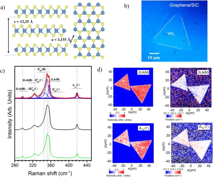
then transferred onto graphene/SiC [25] (more details about the transfer procedure are given in the supplementary information Section I) [26]. A schematic of WS2 crystal structure is presented in Figure 1(a) where the lattice
constants are indicated. The CVD growth of WS2 on SiO2 results in characteristic single-crystal domains shaped as
well-defined equilateral triangles [27]. These films can be nondestructively transferred to various kinds of substrates as desired. With respect to SiO2 and similar substrates, graphene layer has favorable qualities such as atomic
flatness, and homogeneous charge distribution. This should enable direct investigation of the adjacent TMD’s intrinsic electronic structure and many-body effects. Graphene layer is often used as a substrate for TMD heterostructures with high device performance [28]. Single layered WS2 flakes were then easily identified by their
optical contrast with respect to the graphene substrate (Figure 1(b)) and confirmed by micro-Raman spectroscopy
(Figure 1 (c) and (d)). The optical image in Figure 1(b) shows large (lateral size about 50 μm) triangular flakes of
WS2 on the graphene layer. The graphene underlayer used in this study was obtained by annealing 4H-SiC(0001)
(see Methods). After the transfer of WS2 onto graphene, an annealing process at T = 300 °C for 60 minutes in UHV
was used to further clean the surface and interface of the WS2/graphene heterostructure. To investigate the structural
properties of the WS2 flakes micro-Raman and photoluminescence (PL) spectroscopy were used (Figure 1 (c) and
(d) and supplementary information section II and III). Several Raman spectra of WS2 on graphene, collected in
different flake positions, are shown in Figure 1(c). These Raman spectra are obtained with 532 nm excitation, which is in resonance with the B exciton absorption peak [29,30] . Then, beside the first order modes at the Brillouin zone (BZ) center (Γ), the in-plane phonon mode 𝐸2𝑔1 at 356 cm-1 and the out-of-plane phonon mode A1g at 418 cm- 1 [31,32], the Raman spectra present a series of overtone and combination peaks. These different contributions are
clearly separated using a multi-peak Lorentzian fit (blue lines in Figure 1 (c) top). In particular, the Raman feature around 350 cm-1 is the convolution of several components: the 𝐸
2𝑔1 (𝛤), the 2 LA (M) mode at 351.7 cm-1, which is a
second-order Raman mode due to LA phonons at the M point of the BZ zone, and the 𝐸2𝑔1 (𝑀) mode [33].
Moreover, Raman peaks at 323.7 cm-1 and 297.1 cm-1 are combinations modes, which are attributed to 2𝐿𝐴 (𝑀) −
𝐸2𝑔2 (𝛤) and the 2𝐿𝐴 (𝑀) − 2𝐸2𝑔2 (𝛤) modes, respectively. Raman mapping was conducted to investigate the
uniformity within the single flake. The 2𝐿𝐴 (𝑀), 𝐸2𝑔1 (𝛤) and the A1g (𝛤) modes intensity and position mapping are
shows in Figure 1(d) and S2. These Raman modes peak positions and intensity are uniform within the single crystal, indicating that the electronic properties of WS2 are uniform on the graphene substrate. From the frequency
average distance of 65.9 ± 0.1 cm-1 is obtained, as shown in figure S4. This value is consistent with monolayer WS 2
as already shown by previous studies [37]. For the following experiments, the single layer coverage was estimated to be around 20% of the total area of the sample.
The high quality of the WS2 transferred on graphene layer allows investigating the electronic structure by X-ray
photoelectron spectroscopy (XPS) and ARPES. Both the feasible large-area synthesis and the reliable film transfer process can promise that WS2 ultrathin films will pave a route to many applications of 2D materials and vdW
heterostructure. XPS is used to determine the chemical composition and stoichiometry of the WS2 films transferred
on the graphene. The C-1s XPS spectrum of WS2/graphene heterostructure, collected at h=340 eV, is shown in
Figure 2(a). The C-1s spectrum showed three components at 283.9, 284.7, and 285.1 eV in binding energy (BE).
These components correspond to the SiC bulk (labeled SiC), the graphene layer (labeled G), and the interface layer (labeled I), respectively. The G peak was fitted by a sum of a Gaussian function convoluted with a Doniach-Sunjic line shape with an asymmetry factor of 0.09 and a FWHM of 0.4 eV. The low value of the FWHM indicates that only one core level peak was present and thus the carbon atoms had a unique chemical environment. Moreover, no structure appeared at 286.7 eV in the C-1s XPS spectrum, usually attributed to the contamination and/or oxidation, this means even if the samples were annealed at 300 °C, the WS2/graphene layers were very inert and did not show
any contaminationafter WS2 transfer process.
The W-4f and S-2p XPS peaks deconvolution shown in Figure 2(b) and (c), present the standard WS2 stoichiometry.
The WS2 is well fitted by a doublet peaks at BE of 33.4 eV, 35.6 eV, corresponding to W-4f7/2, W-4f5/2 core energy
levels (4f5/2: 4f7/2 ratio of 0.75) [38], respectively (Figure 2(b)). The sulfur S-2p peak (Figure 2(c)) consists of a
single doublet (S 2p3/2 at a BE = 163 eV and a 2p1/2:2p3/2 ratio of 0.5 and spin-orbit splitting of 1.19 eV)
corresponding to S-W bonding, and confirms the presence of WS2. The absence of the oxygen content [39,40] in
these samples is a result of high quality of the interface in this hybrid hetero-structure, particularly in light of the Raman characteristics that are comparable to high quality WS2 (see above and supplementary information section II
and ref [41]).
The electronic structure was also probed using ARPES measurements. The WS2 flakes are relatively well spaced on
the graphene substrate, ensuring, thanks to the small spot size (50×50 m2), the mapping of a single flake. Figure
2(d) shows the photoelectron intensity as a function of energy and k-momentum around the normal emission. This is a good measure of the band structure of WS2 around Γ. The zero of binding energy (i.e. the Fermi level) was
determined by fitting the leading edge of the graphene layer at the same photon energies and under the same experimental conditions. Beside the typical dispersion of the π bands of graphene around -6 to -8 eV (most intense band), a new set of bands is visible at the Γ point of the BZ, which is the signature of WS2 valence band. In the
spectra, the most distinct features include the valence band maximum (VBM) at . The full width at half maximum (FWHM) of WS2 band branches is about 80 meV as shown by Energy distribution curves (EDC) in Figure S7)
extracted from the ARPES map of Figure 2(d) at the point. The sharpness of the different bands can be attributed to the high quality of the transferred flake. Figure 2(e) shows the measured band structure corresponding to the graphene underlayer. The single and robust Dirac cone confirms that the graphene monolayer at the heterostructure preserves the Dirac linear dispersion and the massless relativistic character of the graphene carriers close to the Fermi level. The Dirac point (ED) is located at 0.40 eV below the Fermi level as in the case of pristine graphene on
SiC [12]. Then, the n-type doping, close to 9×1012 cm−2, of pristine graphene was not modified by the formation of
Figure S8), that there was no significant charge transfer between the 2D materials. However, if we look more in detail at the momentum distribution curves (MDCs) shown in figure 2 (f) a less dispersive behavior of the peaks are present around ED. Then, the presence of gap-like feature at the K point (already present in the pristine graphene)
cannot be completely excluded [42]. However, a more detail study of this feature goes beyond the scope of this paper. From a linear fitting of the MDCs a Fermi velocity vF~ 1.05 × 10⁶ m/s was also determined.
It is obvious that also the sharp and intense structure of -bands confirms the high structural quality of WS2 /
graphene heterostructure. Differently from our previous work on MoS2/graphene layer and from Diaz et al. [12,43]
no signature of interlayer hybridization and mini-gaps opening [44] is present on the π-band of graphene. The absence of this superperiodicity effects probably is related to the mismatch angle between the WS2 flake and the
graphene underlayer. In the following discussions regarding the ARPES data, we will focus mostly on the split of the valence band feature at the K-point of the WS2 (Figures 3). In particular, in order to gain more insight on the
electronic structure of WS2, we performed first principles electronic structure calculations on an isolated WS2
monolayer using the QUANTUM ESPRESSO code [45,46] and PBE [47] and HSE06 [48] hybrid functionals within the adaptive compressed exchange [49] implementation. More technical details are given in the supplemental materials (section IV). Figure 3(a) shows the measured band structure around the K valley. The top of the valence band at the K point is mostly formed by planar dxy and dx2-y2 orbital of tungsten, while at the point the band is
mostly composed by W dz orbitals and Spz orbitals.
The observation of a single valence band at with a higher binding energy than at K also excludes the contribution from bilayer or trilayer WS2: in bilayer TMD systems, the valence band near shows a bonding/anti-bonding
splitting that would be observable by ARPES as two bands, in contrast to what is seen here [15]. The maximum of the valence band is located at the K point (-1.8 eV, which is 0.3 eV higher than at point). Since the band gap of single WS2 is 2.27 eV [50], these measurements indicate that our sample is heavily electron doped, which is
consistent with previous reports. [51] The electronic structure in the -2 eV to -3 eV binding energy range is globally in good agreement with our electronic structure calculations (Figures 3(b) and (c)), although the energy separation between the top of the valence band at K and is slightly underestimated in PBE (Figure 3 (b)). In both theory and experiments the valence band maximum at the point is located at higher binding energies than that at the K-point, the energy separation between the two being 0.20 eV in experiments (Figure 3(b) and (c)), 0.17 eV in PBE and 0.20 eV in HSE Figure 3 (c). The measured spin-orbit splitting at K is about 440 meV. Our theoretical calculations for the isolated WS2 monolayer lead to splittings of 440 meV (PBE) and 551 meV (HSE06 on top of PBE).
Moreover, an analysis of the curvature of the bands from the ARPES measurements also allows us to deduce the effective mass of the single layer WS2 forming the heterostructure. We determined an experimentally derived hole
effective mass of 0.4 m0 (upper band) and 0.5 m0 (lower band) (where m0 is the free electron mass) at K, and a hole
effective mass of 1.7 m0 at . These values agree very well with the PBE calculated bands, suggesting that many
body effects are not important close to the top of the valence band at K.
Finally, the gap between the two highest energy valence bands and the bands at lower energies is substantially underestimated in PBE. The inclusion of the exchange interaction within the HSE06 functional on top of the PBE geometry corrects both errors but leads to a somewhat too large spin-orbit coupling.
Although we cannot include explicitly the interaction with the substrate as we miss the structural orientation between WS2 and graphene, it seems that the measured ARPES data agrees well with the bands of an isolated single
particular the exchange interaction seems to improve the agreement not only for the top of the valence band at zone center but also for the electronic structure in the binding energy region below -3 eV.
IV. CONCLUSIONS
In summary, we have studied the electronic structure of single layer WS2 on epitaxial graphene. We found that this
heterostructure gives rise to sharp bands, in particular for the WS2 VBM near the and K points. We directly
observe the strong spin splitting of the upper VB and its value are in excellent agreement with the PBE DFT calculations. Our ARPES measurements on the heterostructure showed graphene and WS2 largely retained their
original electronic structure and, in particular suspended WS2 monolayer is a good approximation of the electronic
properties close to the top of the valence band. Finally, we determined experimentally spin-orbit splitting. Our results provide an important reference for future studies of electronic properties of WS2 and their applications in
spintronic and valleytronic devices
Acknowledgements: We acknowledge support from the Agence Nationale de la Recherche (ANR) under grants
Labex Nanosaclay and H2DH (ANR-15-CE24-0016), from the Region Ile-de-France in the framework of C’Nano IdF (nanoscience competence center of Paris Region). Labex Nanoscalay belongs to the public funded Investissements d’Avenir program managed by ANR.
Figure captions:
Figure 1: Structural and electronic properties of a WS2/graphene heterostructure: a) crystalline structure of
WS2, b) typical optical image of the WS2 transferred onto the graphene layer. The contrast has been adjusted in
order to improve the visibility of the flake. The WS2 profile is traced by white dashed lines, c) micro-Raman spectra
taken on different position of the WS2/graphene heterostructure, in the top spectrum the used multi-peak Lorentzian fit is shown as blue lines, d) Raman maps images of the peak intensity and position of the 2LA(M) (top) and A1g
Figure 2: High resolution XPS and ARPES of WS2/graphene heterostructures: a) C-1s and b) W-4f , (e) S-2p
core levels at h = 340 eV.d) ARPES map of WS2/graphene heterostructure around the point in the K high
symmetry direction of WS2 Brillouin zone, e) Band structure of the graphene layer in the heterostructure at the K
high symmetry direction, f) corresponding momentum distribution curves (MDCs) of figure (e).
Figure 3: a) ARPES map of single layer WS2 along the K high symmetry directions, b) and c) Comparison
References
[1] A. K. Geim and I. V. Grigorieva, Van der Waals heterostructures., Nature 499, 419 (2013).
[2] H. Li, Q. Zhang, C. C. R. Yap, B. K. Tay, T. H. T. Edwin, A. Olivier, and D. Baillargeat, From Bulk to Monolayer MoS2: Evolution of Raman Scattering, Adv. Funct. Mater. 22, 1385 (2012).
[3] E. V Castro, K. S. Novoselov, S. V Morozov, N. M. R. Peres, J. M. B. L. Santos, J. Nilsson, A. K. Geim, and A. H. C. Neto, Biased Bilayer Graphene : Semiconductor with a Gap Tunable by the Electric Field Effect, Phys. Rev. Lett. 99, 216802 (2007).
[4] L. Yang, N. a. Sinitsyn, W. Chen, J. Yuan, J. Zhang, J. Lou, and S. A. Crooker, Long-lived nanosecond spin relaxation and spin coherence of electrons in monolayer MoS2 and WS2, Nat. Phys. 11, 830 (2015).
[5] J. He, D. He, Y. Wang, and H. Zhao, Probing effect of electric field on photocarrier transfer in graphene-WS_2 van der Waals heterostructures, Opt. Express 25, 1949 (2017).
[6] G. Froehlicher, E. Lorchat, and S. Berciaud, Charge Versus Energy Transfer in Atomically Thin Graphene-Transition Metal Dichalcogenide van der Waals Heterostructures, Phys. Rev. X 8, 11007 (2018).
[7] E. Pallecchi, F. Lafont, V. Cavaliere, F. Schopfer, D. Mailly, W. Poirier, and A. Ouerghi, High Electron Mobility in Epitaxial Graphene on 4H-SiC(0001) via post-growth annealing under hydrogen., Sci. Rep. 4, 4558 (2014).
[8] T. Georgiou, R. Jalil, B. D. Belle, L. Britnell, R. V Gorbachev, S. V Morozov, Y.-J. Kim, A. Gholinia, S. J. Haigh, O. Makarovsky, et al., Vertical field-effect transistor based on graphene-WS2 heterostructures for flexible and transparent electronics, Nat. Nanotechnol. 8, 100 (2012).
[9] Z. Hu, Q. Liu, S. Chou, and S. Dou, Advances and Challenges in Metal Sulfides / Selenides for Next-Generation Rechargeable Sodium-Ion Batteries, Adv. Mater. 1700606, 1 (2017).
[10] S. Ulstrup, J. Katoch, R. J. Koch, D. Schwarz, S. Singh, K. M. McCreary, H. K. Yoo, J. Xu, B. T. Jonker, R. K. Kawakami, et al., Spatially Resolved Electronic Properties of Single-Layer WS2 on Transition Metal Oxides, ACS Nano 10, 10058 (2016).
[11] J. Katoch, S. Ulstrup, R. J. Koch, S. Moser, K. M. McCreary, S. Singh, J. Xu, B. T. Jonker, R. K. Kawakami, A. Bostwick, et al., Giant spin-splitting and gap renormalization driven by trions in single-layer WS$_2$/h-BN heterostructures, arXiv 1 (2017).
[12] D. Pierucci, H. Henck, J. Avila, A. Balan, C. H. Naylor, G. Patriarche, Y. J. Dappe, M. G. Silly, F. Sirotti, A. T. C. Johnson, et al., Band alignment and minigaps in monolayer MoS2-graphene van der Waals heterostructures, Nano Lett. 16, 4054 (2016).
[13] A. Grubišić Čabo, J. A. Miwa, S. S. Grønborg, J. M. Riley, J. C. Johannsen, C. Cacho, O. Alexander, R. T. Chapman, E. Springate, M. Grioni, et al., Observation of Ultrafast Free Carrier Dynamics in Single Layer MoS 2, Nano Lett. 15, 5883 (2015).
[14] W. Jin, P. Yeh, N. Zaki, D. Chenet, G. Arefe, Y. Hao, A. Sala, T. O. Mentes, J. I. Dadap, A. Locatelli, et al., Tuning the electronic structure of monolayer graphene / MoS 2 van der Waals heterostructures via interlayer twist201409, 1 (2015).
[15] P. C. Yeh, W. Jin, N. Zaki, D. Zhang, J. T. Liou, J. T. Sadowski, A. Al-Mahboob, J. I. Dadap, I. P. Herman, P. Sutter, et al., Layer-dependent electronic structure of an atomically heavy two-dimensional dichalcogenide, Phys. Rev. B - Condens. Matter Mater. Phys. 91, 1 (2015).
[16] S. Forti, A. Rossi, H. Büch, T. Cavallucci, F. Bisio, A. Sala, T. O. Menteş, A. Locatelli, M. Magnozzi, M. Canepa, et al., Electronic properties of single-layer tungsten disulfide on epitaxial graphene on silicon
carbide, Nanoscale 9, 16412 (2017).
[17] A. Rossi, D. Spirito, F. Bianco, S. Forti, F. Fabbri, H. Büch, A. Tredicucci, R. Krahne, and C. Coletti, Patterned tungsten disulfide/graphene heterostructures for efficient multifunctional optoelectronic devices, Nanoscale 10, 4332 (2018).
[18] K. Liu, Q. Yan, M. Chen, W. Fan, Y. Sun, J. Suh, D. Fu, S. Lee, J. Zhou, S. Tongay, et al., Elastic Properties of Chemical-Vapor-Deposited Monolayer MoS2 , WS2 , and Their Bilayer Heterostructures, Nano Lett. 14, 5097 (2014).
[19] M. T. Dau, C. Vergnaud, A. Marty, F. Rortais, C. Beigné, H. Boukari, E. Bellet-Amalric, V. Guigoz, O. Renault, C. Alvarez, et al., Millimeter-scale layered MoSe2 grown on sapphire and evidence for negative magnetoresistance, Appl. Phys. Lett. 110, 11909 (2017).
[20] T. L. E. Strategy, K. Chen, X. Wan, J. Wen, W. Xie, Z. Kang, X. Zeng, and C. E. T. Al, Electronic Properties of MoS2- WS2 Heterostructures Synthesized with Two-Step Lateral Epitaxial Strategy, ACS Nano 9, 9868 (2015).
[21] X. Zhang, F. Meng, J. R. Christianson, C. Arroyo-Torres, M. a Lukowski, D. Liang, J. R. Schmidt, and S. Jin, Vertical heterostructures of layered metal chalcogenides by van der Waals epitaxy., Nano Lett. 14, 3047 (2014).
[22] H. Sediri, D. Pierucci, M. Hajlaoui, H. Henck, G. Patriarche, Y. J. Dappe, S. Yuan, B. Toury, R. Belkhou, M. G. Silly, et al., Atomically Sharp Interface in an h-BN-epitaxial graphene van der Waals Heterostructure., Sci. Rep. 5, 16465 (2015).
[23] E. Pallecchi, M. Ridene, D. Kazazis, C. Mathieu, F. Schopfer, W. Poirier, D. Mailly, and A. Ouerghi, Observation of the quantum Hall effect in epitaxial graphene on SiC(0001) with oxygen adsorption, Appl. Phys. Lett. 100, 253109 (2012).
[24] D. Pierucci, H. Sediri, M. Hajlaoui, E. Velez-fort, Y. J. Dappe, M. G. Silly, R. Belkhou, A. Shukla, F. Sirotti, N. Gogneau, et al., Self-organized metal – semiconductor epitaxial graphene layer on off-axis 4H-SiC ( 0001 ), Nano Res. 8, 1026 (2015).
[25] D. Pierucci, H. Henck, C. H. Naylor, H. Sediri, E. Lhuillier, A. Balan, J. E. Rault, Y. J. Dappe, F. Bertran, P. Le Févre, et al., Large area molybdenum disulphide - epitaxial graphene vertical Van der Waals heterostructures, Sci. Rep. 6, 26656 (2016).
[26] See Supplemental Material at [URL will be inserted by publisher] for details on the fabrication process, measurements and calculations.
[27] G. H. Han, N. J. Kybert, C. H. Naylor, B. S. Lee, J. Ping, J. H. Park, J. Kang, S. Y. Lee, Y. H. Lee, R. Agarwal, et al., Seeded growth of highly crystalline molybdenum disulphide monolayers at controlled locations., Nat. Commun. 6, 6128 (2015).
[28] F. Schwierz, J. Pezoldt, and R. Granzner, Two-dimensional materials and their prospects in transistor electronics, Nanoscale 7, 8261 (2015).
[29] M. O’Brien, N. McEvoy, D. Hanlon, T. Hallam, J. N. Coleman, and G. S. Duesberg, Mapping of Low-Frequency Raman Modes in CVD-Grown Transition Metal Dichalcogenides: Layer Number, Stacking Orientation and Resonant Effects, Sci. Rep. 6, 19476 (2016).
[30] W. Zhao, Z. Ghorannevis, K. K. Amara, J. R. Pang, M. Toh, X. Zhang, C. Kloc, P. H. Tan, and G. Eda, Lattice dynamics in mono- and few-layer sheets of WS2 and WSe2, Nanoscale 5, 9677 (2013).
[31] Y. Kobayashi, S. Sasaki, S. Mori, H. Hibino, Z. Liu, K. Watanabe, T. Taniguchi, K. Suenaga, Y. Maniwa, and Y. Miyata, Growth and Optical Properties of High-Quality Monolayer WS 2 on Graphite, ACS Nano 9,
4056 (2015).
[32] H. R. Gutie, N. Perea-lo, A. Laura, A. Berkdemir, B. Wang, and M. Terrones, Extraordinary Room-Temperature Photoluminescence in Triangular WS 2 Monolayers(2013).
[33] A. Molina-Sánchez and L. Wirtz, Phonons in single-layer and few-layer MoS2 and WS2, Phys. Rev. B 84, 155413 (2011).
[34] A. Berkdemir, H. R. Gutiérrez, A. R. Botello-Méndez, N. Perea-López, A. L. Elías, C.-I. Chia, B. Wang, V. H. Crespi, F. López-Urías, J.-C. Charlier, et al., Identification of individual and few layers of WS2 using Raman spectroscopy., Sci. Rep. 3, 1755 (2013).
[35] F. Withers, T. H. Bointon, D. C. Hudson, M. F. Craciun, and S. Russo, Electron transport of WS2 transistors in a hexagonal boron nitride dielectric environment, Sci. Rep. 4, 4967 (2015).
[36] G. V. Bianco, M. Losurdo, M. M. Giangregorio, A. Sacchetti, P. Prete, N. Lovergine, P. Capezzuto, and G. Bruno, Direct epitaxial CVD synthesis of tungsten disulfide on epitaxial and CVD graphene, RSC Adv. 5, 98700 (2015).
[37] F. Withers, T. H. Bointon, D. C. Hudson, M. F. Craciun, and S. Russo, Electron transport of WS2 transistors in a hexagonal boron nitride dielectric environment, Sci. Rep. 4, 4967 (2015).
[38] X. Mao, Y. Xu, Q. Xue, W. Wang, and D. Gao, Ferromagnetism in exfoliated tungsten disulfide nanosheets, Nanoscale Res. Lett. 8, 430 (2013).
[39] Y. Li, D. Chen, and R. A. Caruso, Enhanced electrochromic performance of WO3 nanowire networks grown directly on fluorine-doped tin oxide substrates, J. Mater. Chem. C 4, 10500 (2016).
[40] D. Barrera, Q. Wang, Y.-J. Lee, L. Cheng, M. J. Kim, J. Kim, and J. W. P. Hsu, Solution synthesis of few-layer 2H MX2 (M = Mo, W; X = S, Se), J. Mater. Chem. C 5, 2859 (2017).
[41] Y. Gao, Z. Liu, D.-M. Sun, L. Huang, L.-P. Ma, L.-C. Yin, T. Ma, Z. Zhang, X.-L. Ma, L.-M. Peng, et al., Large-area synthesis of high-quality and uniform monolayer WS2 on reusable Au foils6, 8569 (2015). [42] S. Y. Zhou, G.-H. Gweon, A. V. Fedorov, P. N. First, W. A. De Heer, D.-H. Lee, F. Guinea, A. H. C. Neto,
and A. Lanzara, Substrate-induced bandgap opening in epitaxial graphene., Nat. Mater. 6, 770 (2007). [43] H. Coy Diaz, R. Addou, and M. Batzill, Interface properties of CVD grown graphene transferred onto
MoS2(0001)., Nanoscale 6, 1071 (2014).
[44] H. C. Diaz, J. Avila, C. Chen, R. Addou, M. C. Asensio, and M. Batzill, Direct observation of interlayer hybridization and Dirac relativistic carriers in graphene/MoS₂ van der Waals heterostructures., Nano Lett.
15, 1135 (2015).
[45] P. Giannozzi, S. Baroni, N. Bonini, M. Calandra, R. Car, C. Cavazzoni, D. Ceresoli, G. L. Chiarotti, M. Cococcioni, I. Dabo, et al., QUANTUM ESPRESSO: a modular and open-source software project for quantum simulations of materials., J. Phys. Condens. Matter 21, 395502 (2009).
[46] O. Andreussi, T. Brumme, O. Bunau, M. Buongiorno Nardelli, M. Calandra, R. Car, C. Cavazzoni, D. Ceresoli, M. Cococcioni, N. Colonna, et al., Advanced capabilities for materials modelling with Quantum ESPRESSO, J. Phys. Condens. Matter (2017).
[47] J. P. Perdew, K. Burke, and M. Ernzerhof, Generalized Gradient Approximation Made Simple [Phys. Rev. Lett. 77, 3865 (1996)], Phys. Rev. Lett. 78, 1396 (1997).
[48] A. V. Krukau, O. A. Vydrov, A. F. Izmaylov, and G. E. Scuseria, Influence of the exchange screening parameter on the performance of screened hybrid functionals, J. Chem. Phys. 125, 224106 (2006).
[49] L. Lin, Adaptively Compressed Exchange Operator, J. Chem. Theory Comput. 12, 2242 (2016).
Korn, et al., Coulomb engineering of the bandgap and excitons in two-dimensional materials, Nat. Commun.
8, 15251 (2017).
[51] S. Ulstrup, A. G. Čabo, D. Biswas, J. M. Riley, M. Dendzik, C. E. Sanders, M. Bianchi, C. Cacho, D. Matselyukh, R. T. Chapman, et al., Spin and valley control of free carriers in single-layer WS2, Phys. Rev. B 95, 1 (2017).