Dielectric Sensing of Silicon Accelerometers
by
Bethany Ruth Kroese
Submitted to the Department of Electrical Engineering and Computer
Science
in partial fulfillment of the requirements for the degree of
Master of Engineering in Electrical Engineering and Computer Science
at the
MASSACHUSETTS INSTITUTE OF TECHNOLOGY
September 2013
@2013
Massachusetts Institute of Technology. All rights reserved.
The author hereby grants to MIT permission to reproduce and to distribute publicly paper and electronic copies of this thesis document in whole or in part in any
medium now known or hereafter created.
AH £-TTS INSTrfUTE
OCT
292013
Author
..
. ...
.. i -BRA R IES
'...
Department of Electrical Engineering and Computer SCience
August 23, 2013
Certified by....
...
Dana Weinstein
Associate Professor of Electrical Engineering and Computer Science
A
Thesis Supervisor
A ccepted by ....
...
Professor Albert R. Meyer
Chairman, Masters of Engineering Thesis Committee
Dielectric Sensing of Silicon Accelerometers
by
Bethany Ruth Kroese
Submitted to the Department of Electrical Engineering and Computer Science on August 23, 2013, in partial fulfillment of the
requirements for the degree of
Master of Engineering in Electrical Engineering and Computer Science
Abstract
Microaccelerometers have established themselves as a vital piece of the global micro-electromechanical systems (MEMS) market with applications spanning automotive, industrial, military, biomedical, and consumer electronics sectors. They remain one of the top-selling silicon sensors, with $1.6 billion in revenue reported in 2011 equating to 15% of the total MEMS market.
[1]
Continued, expected growth in the next few years demands innovation to meet new industry requirements. Current commercial accelerometer designs are based on a differential capacitor structure which measures the change in capacitance between a set of interdigitated fingers. These fingers are separated by air gaps in high aspect ratio, suspended polysilicon microstructures. Despite its widespread use, the air gap capacitor has some significant drawbacks. It involves a release step during fabrication which introduces complexity and variation in the devices. In addition, these transducers are subject to pull in and stiction which can render a device inoperable. Air gap devices are vulnerable to particulates requiring complicated packaging steps which increase cost and yield of production. Moreover, these devices are also subject to electrical drift. All of these issues can be addressed by replacing this air gap with a dielectric. Not only does it mitigate these concerns, it also offers potential for smaller device footprint, more robust design, and increased shock survival. This project developed a new accelerometer design sand-wiching a thin film dielectric between two electrodes. This capacitor was patterned on top of a bending flexure which supported a large hanging mass. In the presence of an external acceleration, the deflection of the suspension beams caused a deformation of the dielectric film resulting in a change in capacitance. Fabrication using an SOI substrate allowed for increased deflection and process control.Thesis Supervisor: Dana Weinstein
Acknowledgments
I dove head first into the world of MEMS and gained valuable experience over the
last year. Each phase brought a new set of challenges and there are many people I would like to thank for helping me tackle each one.
First of all, I would like to thank my advisor, Dana Weinstein, for this research opportunity. Her guidance and motivation have been a constant source of inspiration over the past year.
Next, I would like to thank my labmates: Laura Popa, Bichoy Bahr, Radhika Marathe, Wentao Wang, Siping 'Spin' Wang, Subra Sundaram, Steven Yee, and Wen-Chien Chen. A special thanks to Laura for her input with design and layout. The cleanroom has quite a learning curve and I am grateful to Wentao, Radhika, Subra, and Laura for their help with fabrication. In addition, I would like to thank Bichoy for his help with testing and Spin for his input on simulations. I wish them all success in their research careers and beyond.
Without the MTL staff I would not be where I am today. Whether a tool was acting up or a process didn't go according to plan, there was always someone willing and able to help. A heartfelt thanks to Vicky Diadiuk, Paul Tierney, Eric Lim, Bernard Alamariu, Paudely Zamora, Kurt Broderick, Donal Jamieson, Bob Bicchieri, and Dave Terry for all their patience and assistance. I also want to send a special shout-out to Dennis Ward, for his help with 'all-things-TRL' answering my 'quick questions' all day, everyday. My fellow MTL researchers were a wealth of experience and insight into the cleanroom nuances and I appreciate all their input during this project.
I would also like to extend a special thanks to Analog Devices and Eugene Hwang for their ongoing assistance in accelerometer testing as well as Jamie Teherani for initial probe station training.
Finally, I would like to thank my friends and family. Their unconditional encour-agement, love, and support has kept me going despite many late nights 'drinking from the fire hose.'
Contents
1 Introduction 15 1.1 Motivation . . . . 15 1.2 Introduction to Accelerometers . . . . 17 1.2.1 Fundamental Operation . . . . 17 1.2.2 Basic Structure . . . . 17 1.2.3 Accelerometer Behavior . . . . 18 1.2.4 Design Considerations . . . . 191.3 The Proposed Design . . . . 21
2 Design and Performance 23 2.1 Concept of Operation . . . . 24
2.2 Flexure Designs . . . . 25
2.2.1 Straight Beam Flexure . . . . 26
2.2.2 Top Hat Flexure . . . . 32
2.2.3 W edge Beam Flexure . . . . 38
2.2.4 Pinwheel Flexure . . . . 40
2.3 Three Axis Design . . . . 42
2.4 Device Summary . . . . 47
2.5 Noise Analysis . . . . 51
3 Fabrication 57 3.1 Overview . . . . 57
3.2.1 Potassium Hydroxide Etch of Device Layer
3.2.2 Formation of Capacitors . . .
3.2.3 Plasma Etch of Device Layer. 3.2.4 Buried Oxide Etch . . . .
3.2.5 Silicon Oxide Deposition . . .
3.2.6 Metal Lift-off . . . .
3.3 Back Side Processing . . . . 3.3.1 Nested Mask Patterning .
3.3.2 Handle Wafer Back Etch .
3.3.3 Oxide Removal and Sinter 3.4 Views of Completed Devices . . . . .
3.5 Summary of Process Flow . . . . 4 Testing and Future Work
4.1 Initial Characterization . . . . 4.1.1 Capacitor Testing . . . . 4.2 Future Work . . . . 4.2.1 Accelerometer Testing . . . . 4.3 Conclusion . . . . A Cleanroom Recipes B Layout Reference . . . . 61 . . . . 62 . . . . 64 . . . . 65 . . . . 66 . . . . 67 . . . . 67 . . . . 68 . . . . 70 . . . . 72 . . . . 76 85 . . . . 86 . . . . 87 . . . . 90 . . . . 90 . . . . 91 93 99 . . . . 59
List of Figures
1-1 Mass-Spring-Dashpot System used as a Mechanical Model for an
Ac-celerom eter . . . . 18
1-2 Bode plot for Mass-Spring-Damper System . . . . 20
1-3 Proposed Design for Dielectric Transduction "No Gap" Accelerometer 21 1-4 Comparison of Air Gap and Dielectric Performance . . . . 22
2-1 Deflection of a Straight Beam with Fixed-Guided Boundary Conditions 27 2-2 Straight Beam Design . . . . 28
2-3 Differential Straight Beam Design . . . . 28
2-4 The Maximum Stress and Strain Occur at the Surface Farthest from the Neutral Axis . . . . 29
2-5 Square or Four Beam Design . . . . 30
2-6 Strain of a Straight Beam with Fixed-Guided Boundary Conditions . 31 2-7 Single Capacitor Top Hat Design . . . . 32
2-8 Deflection of a Top Hat with Fixed-Guided Boundary Conditions . . 34
2-9 Radial Strain of a Top Hat with Fixed-Guided Conditions . . . . 36
2-10 Tangential Strain of a Top Hat with Fixed-Guided Conditions . . . . 36
2-11 Differential Design for a Top Hat Device . . . . 37
2-12 W edge Design . . . . 38
2-13 Cross Section of Flexure Beam . . . . 39
2-14 Strain Pattern for Wedge Device . . . . 40
2-15 Examples of Spiral Flexure Design . . . . 41
2-17 2-18 2-19 2-20 3-1 3-2 3-3 3-4
3-5 Straight Sidewall Etch of the Silicon Device 3-6 Metal Contacts after Lift-off . . . .
Nested Mask Patterning . . . .
Final Oxide Removal of BOX . .
Final Tilted View of a Wedge Device Top View of a Beam Device... Top View of Square Devices... Top View of a Differential Beam .
Top View of the Top Hat Devices Top View of a Wedge Device . . . . . Top View of an Unreleased Pinwheel Top View of a Three Axis Device . . Cross Section of an Unreleased Device
. . . . ce . . . . System . . . . Prony Analysis . . 44 46 52 54 Eight Regions of the Two Beam Structure
3 Axis Strain Pattern for a Four Beam Devi
Equivalent Circuit for Mass-Spring-Dashpot Transient Response from Comsol FSI with Cross Sections for Fabrication Process Flow Sloped Sidewall Produced by KOH Etching KOH Etch of the Silicon Device Layer . . Wafer Contact Alignment Marks Added Usi
3-7 3-8 3-9 3-10 3-11 3-12 3-13 3-14 3-15 3-16 3-17 4-1 4-2 4-3 4-4 4-5 4-6 85 86 87 88 90 91 . . . . 58 of <100> Silicon . . . . . 60 . . . . 61 ng a Stepper Mask . . . . 63 Layer . . . . 64 . . . . 66 . . . . 67 . . . . 71 . . . . 71 . . . . 72 . . . . 72 . . . . 73 . . . . 73 . . . . 74 . . . . 74 . . . . 75 . . . . 75
Three Dimensional Views of Device Deflection after Fabrication . . .
Nonideal CV Measurements After Sintering . . . .
CV Characteristics After Handle Wafer Silicon Etch - Device 17 . . . CV Characteristics After Silicon Oxide (BOX) Etch - Device 18 . . .
Bond Pad Assignments for Accelerometer Testing . . . . Testing Set-up for Differential Capacitor Using Synchronous Demodu-lation [2] . . . .
B-1 Beam Layout ... ... 100
B-2 Four Beam (Square) Layout . . . . 100
B-3 Differential Beam Layout . . . . 101
B-4 Top Hat Layout . . . . 101
B-5 Differential Top Hat Layout . . . . 102
B-6 Wedge Layout . . . . 102
B-7 Pinwheel Layout . . . . 103
B-8 Three Axis Layout . . . . 103
B-9 Full Die Layout Including Back Etch . . . . 104
B-10 Die Layout from Top View . . . . 105
List of Tables
2.1 Material Parameters for Comsol Simulations . . . . 26
2.2 Strain Tensor Values for 1g Forces Acting in the X, Y, and Z Directions 43 2.3 All Possible States for the Outside Capacitors . . . . 45
2.4 Valid States for the Outside Three Axis Capacitors . . . . 45
2.5 Device Summary . . . . 48
2.6 Expected Device Performance . . . . 49
2.7 Expected Noise Due to Gas Damping . . . . 55
3.1 Summary of Fabrication Process Flow . . . . 79
3.2 Cleanroom Tool Reference . . . . 83
4.1 Nominal Capacitance Values for the First Completed Die . . . . 89
A. 1 AME5000 Descum . . . . 93
A.2 AME5000 Silicon Nitride Etch . . . . 93
A.3 AME5000 Breakthrough Etch . . . . 94
A.4 AME5000 Polysilicon Etch . . . . 94
A.5 AME5000 Shallow Silicon Oxide Etch . . . . 95
A.6 LAM490 Polysilicon Etch . . . . 95
A.7 STS2 Shallow Silicon Etch . . . . 96
A.8 LAM590-ICL Silicon Oxide Etch . . . . 96
A.9 LAM590-TRL Silicon Oxide Etch . . . . 96
A.10 STS1 Deep Silicon Etch . . . . 97
A. 12 Plasmaquest Silicon Oxide Etch . . . . 98
Chapter 1
Introduction
Acceleration sensors or accelerometers have become an essential component of the electromechanical toolbox. Spanning from industrial applications to consumer elec-tronics, these devices have found a wide range of applications. Chapter one introduces the accelerometer and its basic operation.
Chapter two describes the proposed design for the accelerometer developed in this project. It lists the expected analytical and FEM performance as well as predicted noise signal for this system.
Chapter three describes the fabrication of these devices executed in the Microsys-tems Technology Laboratory (MTL) on MIT's campus.
Chapter four reports the initial testing and data collected from the devices as well as future goals.
1.1
Motivation
Microaccelerometers have established themselves as a vital piece of the global MEMS market. The key to their growth and success has been their versatility. The ability to span a wide variety of specifications in sensitivity, operational range, frequency response, and shock survival has allowed them to adapt to many different technology sectors. Originally commercialized for the automotive industry, they continue to be used for air bag deployment and electronic suspension. They also allow for
indus-trial monitoring of robotics and vibrations as well as military applications in impact
detection and missile control. The development of high resolution accelerometers
fur-ther expanded their reach to activities such as microgravity measurements in space, seismic earthquake prediction, and biomedical observation. Above all, accelerometers
have seen the most growth in the consumer sector spanning areas such as personal navigation, mobile electronics, image stabilization, and virtual reality [3].
MEMS accelerometers remain one of the top-selling silicon sensors, with $1.6
billion in revenue reported in 2011 equating to 15% of the total MEMS market [1].
Inertial sensors have recently seen rapid development in the consumer and mobile
electronics industry with leading manufacturer, ST Microelectronics reporting double digit growth since 2009 [4]. This growth has been made possible by the decreasing
cost and size of the maturing inertial MEMS technology coupled to the explosive take-off of smartphones, tablets, and gaming systems. The continuing demand for "sensor fusion" electronics, using both discrete and combination inertial sensors, promises exciting opportunities and growth for these devices [5] .
Current commercial accelerometer designs, such as those produced by Analog De-vices, are based on a differential capacitor structure which measures the capacitance
between a set of interdigitated fingers. These fingers are separated by air gaps in high
aspect ratio, suspended polysilicon microstructures. Many iterations of this design all use a similar concept measuring the capacitance change across a moving air gap.
Despite its widespread use, the air gap capacitor has some significant drawbacks. It
involves a release step during fabrication which introduces complexity and variation in the devices. Similarly, these transducers are subject to pull in and stiction which can render a device inoperable. In addition, air gap devices are vulnerable to particulates which accumulate and affect the device behavior. To overcome this issue they require complicated packaging steps which increase cost and yield of production. Moreover, these devices are subject to electrical drift. All of these issues can be addressed by
replacing this air gap with a dielectric. Not only does it mitigate these concerns, it
also offers potential for smaller device footprint, more robust design, and increased shock survival.
1.2
Introduction to Accelerometers
Acceleration is the rate of change of velocity measured in units of M/s 2. It is often
described in terms of "g" which is the acceleration due to gravity at sea level (9.81 m/s2). The measurement of acceleration provides valuable information about the motion and orientation of an object.
1.2.1
Fundamental Operation
The fundamental operation of accelerometers are governed by Newton's second law which states
Z
= m*d (1.1)where F is force, m is mass, and a is acceleration. Plainly stated a net force impingent upon a mass will result in a proportional acceleration. In this way acceleration be-comes an important metric in the analysis of a system. Knowledge of both an object's intrinsic parameters (i.e. mass) and its state (i.e. the measured acceleration) provide quantifiable insight of the external environment which is useful in decision-making and control.
1.2.2
Basic Structure
An accelerometer can be broken into three main components: 1) the proof mass sup-ported by a 2) suspension mechanism which is then anchored to a 3) fixed substrate. As external forces act upon the object, in this case the proof mass, the compliant suspension allows the mass to move. In terms of the accelerometer, equation 1.1 can more appropriately be expressed as
a = (1.2)
An accurate measurement of acceleration requires knowledge of both the object's mass and the applied forces. An accelerometer addresses both of these requirements.
The mass is simply described by the proof mass and the net force is extracted from the motion of the device. This motion can be accurately predicted by modeling the compliance of the suspension mechanism governed by Hooke's Law.
Fspring = -k * z (1.3)
Here k is the effective spring constant and z is the displacement of the mass. The device's state is now simplified to a measurement of displacement. Given a known proof mass and model of motion, acceleration measurements can be taken by simply looking at the mass's movement.
1.2.3
Accelerometer Behavior
To model the behavior of this device, the accelerometer can be generalized to a spring-mass-dashpot system as shown in Figure 1-1. Within this model m is the proof mass,
k b
F
Figure 1-1: Mass-Spring-Dashpot System used as a Mechanical Model for an Ac-celerometer
net force is
F = Fapplied + Fspring + Fdamping (1.4) where Fdamping is the damping force or resistance to motion given by
Fdamping = -b * v (1.5)
and v is the velocity of the mass. Using equations 1.3 and 1.5, equation 1.1 becomes
Fapplied - kz - bv = ma
d2z dz
Fapplied = m- ±2 b- + kz (1.6)
dt2 dt
This second order differential equation can also be written using the LaPlace trans-form to describe the transfer function.
F(s) = (Ms2 + bs + k)Z(s)
Z(s) _ 1
F(s) S2+ s 1+.7
m m
Comparing this with the standard second order transfer function
Output(s) Gain
Input(s) s2 + -w-Qs + W2
it is evident that the natural resonant frequency is, w, =, and the quality factor is,
Q
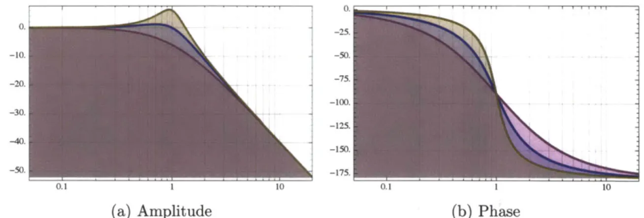
= v7k. Figure 1-2 shows a Bode plot for a generic mass-spring-damper system. Operation should remain within the linear region of this response therefore providinga unity input/output relationship.
1.2.4
Design Considerations
The accelerometer model, outlined in Section 1.2.3, is a powerful tool for evaluating accelerometer designs. At the most basic level these devices are evaluated on
sen-0 . F-.r -25 -10. -50.
100
-125 -40. -150. -50. -175. 0.1 1 10 0.1 1 1(a) Amplitude (b) Phase
Figure 1-2: Bode plot for Mass- Spring-Damper System
sitivity and dynamic range. Sensitivity determines the resolution of the device and the dynamic range describes the bandwidth of operation. Sensitivity, S, is defined as displacement of the mass based on a given acceleration.
S = z (1.9)
a
Assuming that the accelerometer operates at a frequency much lower than the reso-nant frequency, equation 1.7 above can be approximated as
Z(s) 1
A ~ (1.10)
(s)
-thus making the static sensitivity
m 1
S (1.11)
S k W2
The dynamic range of the accelerometer is limited by the natural or undamped reso-nant frequency( T). The device must be operated at a frequency much less than this resonance to ensure that static assumptions hold. Comparing sensitivity and
dynamic range, it is clear that the two performance metrics are inversely propor-tional. A design must take into account the important trade-off between boosting the sensitivity of the device and ensuring an appropriate bandwidth for operation.
1.3
The Proposed Design
This thesis proposes a new design for a capacitively-sensed accelerometer. Shown in Figure 1-3, it consists of a silicon flexure supporting a released proof mass. On
V +
lip_ Polyslillcon V Upe*EjcroG ap Dielectric Doped Silicon Lower ElectrodeFigure 1-3: Proposed Design for Dielectric Transduction "No Gap" Accelerometer
top of the flexure is a dielectric, sandwiched between doped silicon and polysilicon electrodes, to form a capacitor. As the proof mass accelerates in the Z^ direction, the deflection causes a strain in the dielectric along the : direction. Coupled with the Poisson ratio, this strain results in a change in thickness and area for the film thus producing an overall change in capacitance [6]. This design is advantageous to existing devices because it eliminates the need for an air gap instead opting for a robust and compact dielectric.
Given the proposed structure, a silicon-on-insulator (SOI) substrate is a natural choice for fabrication. Traditionally, SOI-MEMS use top side fabrication for devices with in-plane displacement but recent work looked at improving out-of-place deflec-tion with a combinadeflec-tion of high aspect ratio front- and back-side processing [7]. For this proposed design, the device layer is patterned as the flexure supports with the suspended mass made from the handle wafer. The buried oxide layer (BOX) acts as an etch stop as well as provides electrical isolation. Previous work used SOI
tech-nology to build highly sensitive differential accelerometers, but these devices utilized traditional air gap comb actuators for sensing [8]. The proposed devices use a sim-ilar structure choosing instead to pair it with a dielectric sensing mechanism. The different designs were evaluated based on the following metrics.
* AC: The measureable change in capacitance
" AC/C: The capacitance change normalized to its nominal value
" AC/g: The capacitance change normalized to an applied force of gravity
* AC/gA: The capacitance change per area, providing a quasi-density metric
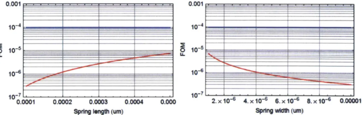
In addition, each device's performance was also calculated based on the following figure of merit.
ACVax Vs2l
FOM = ii (1.12)
2Co aext M
In the case of the air gap capacitor, Vmax is the gap closing voltage and for the dielectric capacitor is the breakdown voltage. Figure 1-4 compares the performance of an air gap capacitor with the newly proposed dielectric design. It is important to note that this new design does not outperform traditional comb drive capacitors. While the design does offer an alternative to existing issues it does come at the cost of some performance. 0.001 - - - - -- 0.001-10-4 10-5 10-6 10-10 __ 4 10-71 L._____ I _ ___. ' I _ I .i 10- . 0.0001 0.0002 0.0003 0.0004 0.000 2. x 10-6 4. x 6. x 10 8. x 0-6 0.00001
Spring ngth (uM) Spring widM (uM)
Figure 1-4: Comparison of Air Gap and Dielectric Performance
4
Chapter 2
Design and Performance
As explained in the last chapter, the proposed device uses capacitors to sense accel-eration. That being said there are many transduction mechanisms which have been used in different designs. The first commercialized design deposited piezoresistive materials on top of the flexing device. As the device moves it imparts a mechan-ical stress on the film changing its resistivity. While the design is simple, devices are susceptible to temperature fluctuations and suffer from low sensitivity [3]. Keep-ing within the electrical domain, piezoelectric materials generate an electrical charge when under compression. Producing minimal deflection and insensitive to electro-magnetic interference, these materials are especially effective in harsh environments, however, they have difficulty with static measurements [9]. Tunneling devices detect variations in tunneling current between two tips. While they are extremely sensitive and compact they require large voltages and are particularly susceptible to noise [3]. In the presence of fluctuating magnetic fields, magnetoresistive accelerometers sense the changes in resistance [10], and Hall Effect devices measure variations in voltage
[11]. Resonant accelerometers take advantage of the change in resonant frequency
produced in a beam under axial loading. These devices are sensitive but limited
by a small operational bandwidth [3]. Accelerometers have also been coupled with
optics using laser sensing or measuring wavelength shifts in fiber optic cables [12]. Designers have even created devices in the thermal domain using thermopiles or tem-perature sensors to measure changes in acceleration. Despite all of these different
techniques capacitively-sensed accelerometers are still the dominate choice. Though susceptible to electromagnetic interference, this transduction mechanism allows for a simple design with low noise, low drift, low power, and insensitivity to temperature
[3]. Different designs are able to span a wide range of applications from high to low sensitivity. Typical capacitive designs involve a vertical or lateral comb drive with interdigitated fingers but the mechanism outlined below offers an alternative which utilizes dielectrics.
2.1
Concept of Operation
The proposed accelerometers are based on the simple physics of a parallel plate ca-pacitor. The equation governing the capacitance of such a device is
EoErA
Co = (2.1)
g
where E0 is vacuum permittivity, Fr is the permittivity of the material, A is the area of the plates, and g is the distance or gap between the two plates. The dielectric transduction accelerometer bases its measurements on a change in capacitance due to the strain imposed on a bending dielectric. This bending, coupled with the Poisson effect, results in a volumetric change in the dielectric summarized by equation 2.2. Here w and 1 are the width and length of the capacitor and g is the thickness of the dielectric.
eoErWdl &oer ldW _ eoer lwd g
dC = + (2.2)
9 9 92
This equation can also be rewritten as
dC = Co* (El +Ew -Eg) (2.3)
where Co is the initial capacitance, el is the strain in length, Ew is the strain in width, and eg is the strain in thickness due to the beam bending. The important thing to note here is that there are three separate terms corresponding to changes in each of
the three dimensions. The first term is the change in length or elongation due to the deflection of the beam. The second two terms are the changes in width and thickness which result from this elongation. For small deflections,
EW -WVE1
Eg -gvc 1 (2.4)
Due to the Poisson effect, changes in width and thickness are of opposite sign com-pared the change in length. Though this suggests that both of these terms hurt the overall capacitance change, it is not the case. The negative sign in the third term of equation 2.3 flips the sign regarding the change in thickness. Thus strain in length and thickness both beneficially add when calculating change in capacitance. This makes sense because as a dielectric elongates it will decrease its width and thickness. While the change in width decreases the overall area of the capacitor the decrease in thickness reduces the gap which is inversely proportional to capacitance.
With this concept in mind there are two cases for a bending dielectric. As scribed above, a film in tension will elongate, thereby shortening its width and de-creasing its gap. This results in a positive change in capacitance. Conversely, a film in compression will shorten its length instead increasing its width and gap resulting in a negative change in capacitance. These two cases can be used to determine the direction of acceleration along an axis.
2.2
Flexure Designs
As described earlier, for static conditions to hold, an accelerometer must be oper-ated at a frequency much lower than its resonant frequency. A high dynamic range therefore pushes for a higher fundamental mode. Unfortunately a higher fundamental mode (oc vk) results in stiffer structures. So devices must work with a lower reso-nant frequency to get more sensitivity. In light of this tradeoff three different target resonant frequencies were selected to define three dynamic ranges: 2 kHz, 5 kHz, and
10 kHz. The major design considerations were twofold. First, a mass and flexure
combination was chosen for each target frequency then the structure's deflection was used to select the appropriate capacitor pattern.
A big consideration for these first generation devices was ensuring a large enough
change in capacitance for the testing apparatus available. To that end the devices were made larger than future iterations. Moreover, further optimization would be possible following the design of an appropriate readout circuit. For this generation of devices an SOI wafer with a 2pm device layer and 500pm handle wafer was chosen therefore fixing the flexure thickness to 2pm. In all the following sections Comsol
simulations assumed the following material parameters.
Table 2.1: Material Parameters for Comsol Simulations
Silicon Polysilicon Silicon Oxide [13] Youngs' Modulus, E [GPa] 170 160 87
Density, p [kg/M 3] 2330 2320 2200
Poisson Ratio, V 0.22 0.22 0.17
Relative Permittivity, Er 11.7 4.5 3.9
2.2.1
Straight Beam Flexure
The basic design for a dielectric transduction accelerometer is a proof mass suspended
by two beams. Each beam, with fixed-guided boundary conditions, can be
character-ized by the following equation for deflection [14].
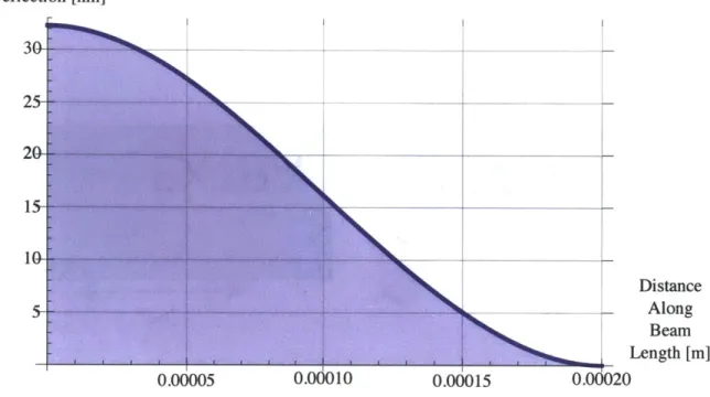
z = (F - )2(l - 2x) (2.5)
12EI
where z is deflection, F is the applied force, E is Young's Modulus, I is moment of inertia, x is distance along the beam starting from the guided end. For a rectan-gular cross section, I = 'h3 . Figure 2-1 shows a sample deflection along the length
12
of the beam. It is important to note that the deflection is antisymmetric across its midpoint. One half of the silicon beam is in tension and the other half is in com-pression. Therefore a dielectric film patterned on top of this beam would see two
Deflection [nm] -5 --- ---Distance 4 Along Beam 7 Length [m] 0.00005 0.00010 0.00015 0.0 20
Figure 2-1: Deflection of a Straight Beam with Fixed-Guided Boundary Conditions
different volumetric changes. The region in tension would elongate resulting in a pos-itive change in capacitance and the region in compression would contract resulting in a negative change in capacitance. With this in mind, a capacitor patterned over the entire beam would be useless producing a zero net capacitance change for any given acceleration. Instead, this characteristic deflection shape was used to develop two types of accelerometers. The first was a single capacitor patterned on one half of each of the two beams to maximize the net change (Figure 2-2). The second, taking advantage of the complementary regions, was two capacitors patterned on each half of the beams allowing for differential sensing (Figure 2-3). Differential measurements offer the benefit of canceling first order effects and providing linearization about a balance point [15].
'Mass
Figure 2-2: Straight Beam Design
Mass
Returning to the bending beam, the radius of curvature, p,
d2Z
Sx2 (2.6)
p [1 + (!L)2 32
can be used to calculate the stress, -, and strain, 61, of the structure. Because the dielectric film is deposited at the farthest distance from the neutral axis (t/2 where t is the beam thickness) maximum stress and strain will be transferred to the film.
Neutral
Axis
Figure 2-4: The Maximum Stress and Strain Occur at the Surface Farthest from the Neutral Axis z 61 = --p Ez p t Emax = 2p Et Umax =-2p (2.7)
The strain equation above describes the elongation of the beam but as stated before the dielectric undergoes a volumetric change. To fully describe the change in capaci-tance the Poisson ratio, v, is applied to calculate strain in the other two dimensions.
fj1/2 cldx AW = -0-vEidy I U I I . = ..
9
Ag = fo-vcldz
Equation 2.3 becomes
dC = CO * (j Ecdx -
j
vedy +j
vedz) (2.9)which is used to describe the performance of the straight beam accelerometer.
Figure 2-5: Square or Four Beam Design
The single capacitor and differential sensor described above are two capacitor patterns for the same flexure-mass structure. Therefore one set of beam parameters was selected for each of the three target frequencies outlined at the beginning of the chapter. The structure for one of these devices is defined by the length, width, and height of the bending beam and mass. With the mass and beam height fixed the other four parameters were varied in a Comsol eigenfrequency analysis to study their dependencies. This study revealed that the high aspect ratio of the suspended mass was dominated by lower swinging pendulum modes. To compensate for this the supporting beams were transitioned to more plate-like structures using 1:2 and 1:4 length-to-width ratios, shown in Figure 2-2, as opposed the to the 10:1 threshold typically used for beams. In another design, two more orthogonal beams were added
to counteract the pendulum behavior creating a set of four beam devices. As shown in the square accelerometer, Figure 2-5, one beam is attached to each side of mass. Not only did the structure offer more stability it also supported larger masses. In addition it allowed for a series of smaller devices with beam-like length-to-width ratios. The selected parameters and device performance are included in Tables 2.5 and 2.6 at the end of the chapter.
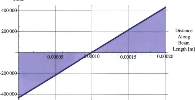
In addition to the flexure modifications, the capacitor pattern was also varied for a set of two beam devices. The plot in Figure 2-6 shows an important gradient; the strain is largest at the edges of the beam. As explained before, this strain is what translates to a change in capacitance. Therefore, provided there is a large enough signal to detect, the performance factor, AC/C, can be improved by reducing the capacitor to a smaller area where there is a larger average strain. This was done for the 5 kHz case reducing the capacitor width by 1/2 and 1/4. The performance for these two devices are also included at the end of the section.
Strain 400000-200000- Distance Along Beam Length [m] .u10 2.015 020 -- 2 0 0 0---_400
2.2.2
Top Hat Flexure
As shown in the last section there are stability issues with the two beam structure. While in theory it is the most sensitive the fundamental pendulum modes limit the size of the mass and the allowable length-to-width ratios for the beams. These restrictions were partially alleviated by moving to a four beam structure also described in the last section. The top hat membrane is the next natural choice for design. It increases the anchor points to the entire circumference of the device. While this design does result in less deflection, it gives the accelerometer more stability in the radial and tangential directions allowing for larger flexure areas and capacitors.
Given the fixed heights these devices are defined by the radius of the mass, rMss,, and the radius of the flexure membrane, rFlex. A larger radius produces a larger the
nominal capacitance and change in capacitance. For first generation devices the total radius was fixed to 700 pm making their size comparable to some of the four beam devices.
Figure 2-7: Single Capacitor Top Hat Design
Deflection in the top hat membrane is now given by the following system of equations assuming an outer fixed boundary and inner guided boundary [14]. Here
a =rMass + rFlex and r is the radial distance from the center. C2 = I _rMass )2 -I -1+ 2 log (a 4 a Mass _ L6 TMass rMass 2 1 4a [ a) -1 Mass C5 = I 1-?Mass )2] 2 [ - a
L3= rMass rMass 2+1 log a rMass 2
4a a rMass a
F2 = F
4=
1[
- ?'Mass 21 + ?'I[1kMassIJ_2_ogG5 = ?'Mass rMass 2 +1 +log rMass 2
-4r r _ \r lineload = F 2ir * rMass plate = * 12(1 - v2) Yb = lineload * a3 C2 * L6 L3 plate C5_ lineload * a * L6 Mb = C5 Mb * F2 2 _ lineload * G3) 3 z = Yb -+ (paer2 lt jr (2.10) plate )plate
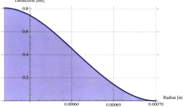
Figure 2-8 shows an example of this deflection. Similar to the straight beam de-sign, it is evident that there are two regions of curvature. Deflection from the mass
causes one ring of the membrane to be in tension and the other to be in compression. This behavior leads to two different types of devices which are included in this lay-out: the single capacitor design and the differential design. The zero from curvature
equation 2.6 with deflection equation 2.10 yields the inflection point of the annular
membrane allowing for the differentiation between the two regions.
ra-Deflection [nm]
Radius [m]
0.06060 0.00065
0.
0Figure 2-8: Deflection of a Top Hat with Fixed-Guided Boundary Conditions
dius, outer, and an inner radius, inner, equation 2.1 becomes
CO = Eoer7r(outer
2 - inner2)
9 (2.11)
and the change in capacitance is described as
(2(outer - inner)dr (outer
2 - inner2)dt _ (outer 2 - inner2)dg
dC = e~r+ 9 9 2 )
(2.12) where dr is radial change, dt is tangential change, and dg as before is the change in thickness.
Single Capacitor Design
The design of the single capacitor device is straightforward. The capacitor is
pat-terned on one half of the membrane making sure not to cross the inflection point. Eigenfrequency analysis showed that the top hat structure and chosen radius did not support a 2 kHz mode. Therefore, three rMass and rFlex combinations were selected
re-spective inflection points were calculated and the capacitors were patterned on the outside area as shown in Figure 2-7. One smaller device with a 400 pm radius and a
11 kHz fundamental frequency was also included.
Like the straight beam design, the capacitor pattern was also varied for the sensi-tive (4 kHz) design. Again assuming fixed outer boundary and guided inner boundary conditions, the axial stress, Orr, and tangential stress, o, are given by the follow sys-tem of equations
[14].
F8 = I [ + v + ( ,v)(rMass) 2
G9 = rMass log( rMaSs 1 + 1 - (rMass 2)]
lineload * a * L6 mRB = C5 mR - (mRB * F8) - (lineload * G9) * r *r = MR (2.13) t2 F5 = I - Mass) 2 G6= TMass rMass 2 1 + Ar _\r / rMass' mRB lieload * G6 theta = * r - n oa r2 thtte ) plate p theta * plate * (1 - V2)
+
* mR r 6 * m9 Oro = t2 (2.14)The strain is given by [16]
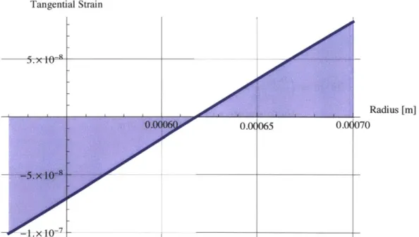
Er = +(E r + 0) c= Ea(Oo + vo-r) (2.15)
Plots in Figure 2-9 and 2-10 again show the strain is largest at the outermost and innermost radii. Therefore the capacitor width of the 4 kHz structure was reduced
Radial Strain t.5.x 10-O.0065 ~,.A I'J Radius [m] 070
Figure 2-9: Radial Strain of a Top Hat with Fixed-Guided Conditions
Tangential Strain
0.00065 0.0(
Radius [m]
070
Figure 2-10: Tangential Strain of a Top Hat with Fixed-Guided Conditions
0.0(
I I
Xt=o-by 1/2 and 1/4. The performance factors for all the single capacitor devices are
summarized in Table 2.5 and 2.6.
Wouter
Figure 2-11: Differential Design for a Top Hat Device
Differential Design
As described previously a differential design is a valuable tool for sensing. The top hat version is shown in Figure 2-11. Ideally both sensing areas of a differential device would have the same nominal capacitance and change in capacitance. Unfortunately it was not possible to match both with the top hat structure. A differential design must have the same change in capacitance to work, so this parameter was the focus of the design. To meet this constraint a system of equations was created using equations 2.11 and 2.12 to simulate the outer and inner capacitors. The outermost radius, a, and innermost radius, rMass, were fixed and the system solved for two radii, router and rinner, which predicted the same capacitance change.
_Eosr7r(rinne, - riass)
InnerCapacitor = oinner - d
_ .E.7r(a 2 - r 2e,
OuterCapacitor = Oouter - d Outer)
dCinner = Co,outer (Cr + CO - Eg)
Mathematica was used to numerically solve dCinner = dCouter for the same three rMass
and rFlex combinations described in Section 2.2.2. Their results are listed in Table 2.5 and 2.6.
2.2.3
Wedge Beam Flexure
WO
Figure 2-12: Wedge Design
The wedge flexure is another variation of the two beam structure from Sec-tion 2.2.1. Like the square and top hat accelerometers, this design worked to stabilize the unwanted pendulum modes by increasing contact with the substrate. Whereas the other two variations increased contact by adding more beams or flexure area, the wedge worked to minimize this increased area therefore maintaining the flexibility of the two beam structure. As shown in Figure 2-12, the straight beam is replaced
by a beam with a tapered width moving from a constant to a linearly-varying cross
section.
Flexural rigidity is defined as, EI, where E is Young's Modulus, and I is the mo-ment of inertia or resistance to motion [17] . Figure 2-13 shows the rectangular cross
section of the beam. Labeled as dashed lines, the beam can bend in two directions resulting in two different moments of inertia, I, and I... The desired and undesired directions of motion are 2 and
y
respectively. In order to make sensitive devices iso-lated in the 2 direction, I, must be minimized and I, must be maximized. Moreover the polar moment of inertia Jr, defined as the summation of I and Iy, affects the pendulum modes and must also be maximized. In the case of the wedge, I varies across the length of the beam and flexural rigidity becomes_ EW(x)h3 EIz(x) = 12 12 Ey (x) - E(X)h (2.16) 12 EJx(x) - Ewjj)h (W(X) 2 + h2)
where the wedge's linearly varying width is described as,
w(x) =(WI -Out)X + Wout (2.17)
lBeam
We can see that both I, and Jx have a cubic dependence on the width while I is only linearly dependent. Therefore, the undesired directions of motion can be stabilized
by increasing the width while only minimally affecting 1. In the case of wedge flexure
this was done by adding triangular tails to the straight beam design thus increasing
wout.
y
Ih
1WOMMONmmmmmmmummuWW
nowm
W(X(a) 2 Strain, ALength (b)
y
Strain, AWidth (c) i Strain, AThicknessFigure 2-14: Strain Pattern for Wedge Device
Figure 2-14 illustrates the strain pattern produced on the top side of a bending wedge. Red indicates a positive strain, green no strain, and blue a negative strain. As expected the largest strain is along the - direction corresponding to the change in length. The next largest contribution, change in thickness 2-14(c), reinforces the change in capacitance according to equation 2.2. Conveniently, the change in width illustrated in 2-14(b), which negatively impacts the capacitance change, is the smallest contribution. Focusing on dominant term, 2-14(a), we see that the inner rectangular area matches the strain pattern produced by a straight beam device. The outer tails, on the other hand, result in an irregular strain pattern. Nonetheless we see that the area of highest strain is the outer and inner fourth of the rectangular portion of the wedge. With this in mind, the capacitor was patterned on the outside fourth of the beam as shown in Figure 2-12 to maximize the capacitance change per area. Three different sets of parameters were chosen corresponding the desired 2 kHz, 5 kHz, and 10 kHz resonant frequencies. Their expected performance is listed in Table 2.5 and 2.6.
2.2.4
Pinwheel Flexure
The last three sets of devices all used flexure mechanisms with an inflection point meaning that one portion of the sensing area was in tension and the other was in compression. While this does offer interesting possibilities for differential sensing, it also limits the size of the capacitor. The pinwheel design ignored differential sensing, and instead worked to eliminate this inflection point thus allowing for the capacitor
*II
Figure 2-15: Examples of Spiral Flexure Design
to be patterned over a larger area. The cantilever is a natural starting point as its deflection along a beam has the same sign of curvature. Unfortunately it is not possible for a cantilever to support a hanging mass as it requires a fixed-free boundary condition. Instead the first iteration of this device moved toward a coiled spring approach which accommodated a compact design for a large beam length. A small torsion bar connected long pliable coils to the mass in an effort to simulate a cantilever-like structure. As expected this design had extremely low resonant modes. Many iterations of two and four coil structures were tested varying dimensions of both the torsion bar and springs. Some examples are shown in Figure 2-15. Given the high aspect ratio of the mass, long springs were unable to provide the necessary stability.
Instead the spiral design converged to a pinwheel structure as shown in the bottom right of Figure 2-15 and also in Figure 2-16. The torsion bar was preserved but the spirals were replaced with a beam. In addition, as was seen with the other designs, higher strain was observed closer to the fixed end of the beam. In response to this the capacitors were patterned on only half of the flexure to increase the expected performance. Two versions were included in the layout and their parameters are listed in Tables 2.5 and 2.6
Wconnect W Beam W~m =30 pm connect =15 pm
Figure 2-16: Pinwheel Design
2.3
Three Axis Design
Force, which causes acceleration, is a vector quantity therefore giving it a magnitude as well as a direction. To describe forces in the three dimensional world a sensor must resolve contributions from three orthogonal axes. The devices outlined above are designed to be sensitive in one direction namely the Z^ axis as outlined in Figure
1-3. That being said acceleration in the real world occurs in all directions so, ideally,
an accelerometer should be able to detect motion from all of these orientations. A study of the basic beam flexure design shows potential for this three axis pick off due to the pendulum behavior of the proof mass.
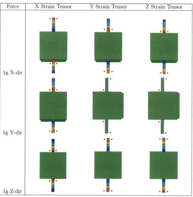
To illustrate this concept Table 2.2 shows the strain distribution in the beams when subject to a force in each of the i,
y,
and directions. Restating the gradient of color, red corresponds to a positive, tensile strain and blue to a negative, compressive strain. Red results in a positive change in capacitance and blue results in a negative one. A powerful pattern forms. To emphasize the pattern plus signs have been added next to all of the positions of positive strain.Table 2.2: Strain Tensor Values for ig Forces Acting in the X, Y, and Z Directions
1g X-dir + +§.
+g
Y-dir + +
1g Z-dir + + + +
Table 2.2 contains a lot of information but there are two levels of redundancy which can be used to simplify this explanation. First, we note by looking at the
columns that a similar pattern manifests in each direction of the strain tensor. This makes sense given the explanation about the Poisson effect in Section 2.1. With this redundancy, we can focus on the pattern formed in one axis. Second, looking at the second row of Table 2.2, we note that each beam can be segmented into four quadrants. Shown in Figure 2-17, there are eight distinct areas which can be used to extract information from the device. Given the boundary conditions of the beams, the inner four areas form the exact opposite pattern as the outer four so we can focus attention to the outer four areas of the device. Thus illustration of the three axes pick off can be simplified to four outer areas of the beams.
1
2
M
A
7
6
S
8
S
3
4
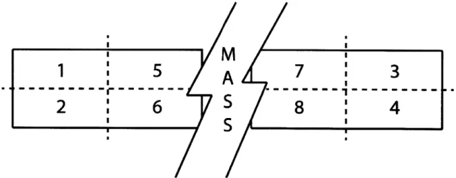
Figure 2-17: Eight Regions of the Two Beam Structure
These four areas provide four distinct signals about the behavior of the device. In reality each signal is a change in capacitance corresponding to a magnitude of acceleration. To get an understanding of the concept we can reduce these signals to a binary representation. Keeping with the color scheme of Table 2.2,
positive change in capacitance (red) -
+
negative change in capacitance (blue) -
-These four signals now give us four bits of information with 24 or 16 possible states. Table 2.3 shows all of the possible states. Given the boundary conditions of the beams those highlighted in red are not valid. Eliminating these states, we are left with eight possibilities each of which correspond to a type of acceleration. Each direction of
Table 2.3: All Possible States for the Outside Capacitors
1 2 3 4
Table 2.4: Valid States for the Outside Three Axis Capacitors
1 2 3 4 Acceleration Type + + + + Negative Z + + - - Positive X + - + - Negative Y + - - + Counterclockwise Torque - + + - Clockwise Torque - + - + Positive Y - - + + Negative X - - - - Positive Z
motion can be distinguished using the patterns formed by the four outside capacitors. Forces in the Z^ direction impose the same strain on all four capacitors. Forces in the 9 or transverse direction produce opposite changes at the two fixed ends and forces in the , or axial direction result in opposite strains across the longitudinal axis.
This analysis' usefulness is twofold. One, these patterns can be used to cancel out forces in the axial and longitudinal directions thus isolating the desired out of plane acceleration. Adding all of the capacitance changes together will result in a zero net change for forces in the axial and longitudinal directions while reinforcing the capacitance change in the sensitive out of plane direction. Two, these signals can
(a) Strain, ALength (b) 9 Strain, AWidth (c) i Strain, AThickness
Figure 2-18: 3 Axis Strain Pattern for a Four Beam Device
also be used to detect accelerations in all three directions. This can done using the lookup table above or by doing a simple inversion of half of the incoming signals and summing all the signals. Use of the inversion scheme will isolate forces in the axial or longitudinal directions while canceling forces in the other directions. The logic is outlined below
1
+
2+
3+
4 -+ ±Zdirection- + 2 + -,3 + 4 -+kYdirection
1 + 2 + -,3 + ,4 -+ kXdirection
The inner capacitors encode redundant information and can be combined in a similar fashion to boost the overall change in capacitance.
In reality it is difficult to route four (outer) or eight (outer and inner) individual capacitors on each device. To remedy this the three axis design was converted to a four beam flexure. Not only did this simplify the routing it also allowed for larger capacitors and more stability in the device as discussed in Section 2.2.1. Figure
2-18 shows the strain pattern produced along one axis. As before an acceleration in
the . direction produces the same change in all four capacitors providing the largest
signal. Negating half of the signals (right and bottom) and adding contributions from opposite beam pairs creates two signals which can be used to extract accelerations in the - and Y directions. Using the same dimensions, a set of square accelerometers were modified for this purpose patterning contacts for each individual capacitor.
2.4
Device Summary
The following two tables summarize the devices included in this first generation of design. The first table lists each device and their appropriate dimensions. Refer to each flexure diagram in Section 2.2 for a description of the parameters. The second table lists each device and their expected performance based on the metrics in Section 1.3. For the figure of merit, Vmax is the breakdown voltage of the dielectric related to the dielectric strength. Assuming 9 nm of silicon oxide with a dielectric strength of 12 * 106 V/cm [13], the breakdown voltage was calculated as 10.8 V.
Table 2.5: Device Summary
Freq Dimensions Footprint
[kHz] [ym] [m
Beam
1 2.05 WBeam:6 0 0 1Beam:2 0 0 IMass:1250 lCap:100 1.98e-6
2 5.01 WBeam:4 0 0 1Beam100 lMass:7 0 0 lcap:50 7.20e-7
3 5.01 WBeam:4 0 0 lBeam:1 0 0 lMass:7 0 0 lcap:25 7.20e-7
4 5.01 WBeam:4 0 0 lBeam:100 lMass:7 0 0 lCap:1 2.5 7.20e-7
5 10.30 WBeam:4 0 0 lBeam:100 Mass: 190 lCap:50 3.12e-7
Differential Beam
6 2.05 wBeam:6 0 0 lBeam:2 0 0 Mass:1250 lCap:100 1.98e-6
7 5.01 wBeam:4 0 0 IBeam:100 lMass:7 0 0 lCap:50 7.20e-7
8 10.30 WBeam:4 0 0 lBeam: 100 Mass 190 Cap:50 3.12e-7 Square
9 2.31 wBeam:2 0 0 lBeam:2 0 0 lMass:9 20 9.14e-7
10 5.04 wBeam:2 0 0 lBeam:100 lMass:9 5 0 9.23e-7
11 10.11 WBeam:4 0 0 lBeam:1 0 0 lMass:850 8.03e-7
12 3.30 WBeam:19 lBeam:80 lMass:500 2.53e-7
13 2.81 WBeam 17 lBeam:90 Mass:4 0 0 1.63e-7
14 2.37 WBeam 14 lBeam:100 lMass:3 0 0 9.28e-8
15 2.51 WBeam 7 lBeam:90 lMass: 2 0 0 4.1le-8 Top Hat
16 3.92 rFle.:2 60 TMass:4 40 wCap: 141.9 1.54e-6
17 3.92 rFlex:2 60 rMass:4 40 wCap:70.9 6 1.54e-6
18 3.92 TFlex 2 60 rMass:4 40 wCap:3 5.4 8 1.54e-6
19 5.02 TFlez 180 rMass:520 wcap:9 6.4 3 1.54e-6 20 10.38 rFlex:105 TMass:595 wCap:55.92 1.54e-6
21 11.04 rFle: 140 rMass:2 60 wCap:3 8.4 8 5.03e-7
Differential Top Hat
22 3.92 TFlex:2 60 rMass:4 40 wot: 13 3.7 w
1 n:122.5 1.54e-6
23 5.02 rFlex: 180 rMass:520 wot:90.56 w1n:85.68 1.54e-6 24 10.38 rFlex:105 TMass:595 wot:51.32 wn:49.77 1.54e-6
Wedge
25 2.03 wot:600 w1n:400 1Beam:2 0 0 lMass:1 250 7.00e-7 26 5.04 wot:600 wIn:400 lBeam 1 0 0 Mass:1 2 0 0 5.80e-7
27 10.11 wot:400 w1n:200 1Beam:50 lMass:7 0 0 1.70e-7
Pinwheel
28 2.01 lBeam:1 7 6.5 wConnect:12 Mass 3 0 0 1.12e-7
29 2.59 lBeam 11 8.5 wConnect:7 lMass:2 0 0 5.46e-8 Three Axis
30 2.03 lMass:9 20
WBeam:2 0 0 lBeam:2 0 0 4.00e-8
31 5.04 lMass:950 WBeam:2 0 0 lBeam:2 0 0 1.50e-8