HAL Id: hal-02145940
https://hal.archives-ouvertes.fr/hal-02145940
Submitted on 3 Jun 2019
HAL is a multi-disciplinary open access
archive for the deposit and dissemination of
sci-entific research documents, whether they are
pub-lished or not. The documents may come from
teaching and research institutions in France or
abroad, or from public or private research centers.
L’archive ouverte pluridisciplinaire HAL, est
destinée au dépôt et à la diffusion de documents
scientifiques de niveau recherche, publiés ou non,
émanant des établissements d’enseignement et de
recherche français ou étrangers, des laboratoires
publics ou privés.
Polarized cathodoluminescence for strain measurement
M. Fouchier, N. Rochat, E. Pargon, Jean-Pierre Landesman
To cite this version:
M. Fouchier, N. Rochat, E. Pargon, Jean-Pierre Landesman. Polarized cathodoluminescence for strain
measurement. Review of Scientific Instruments, American Institute of Physics, 2019, 90 (4), pp.043701.
�10.1063/1.5078506�. �hal-02145940�
Cite as: Rev. Sci. Instrum. 90, 043701 (2019); https://doi.org/10.1063/1.5078506
Submitted: 25 October 2018 . Accepted: 15 March 2019 . Published Online: 08 April 2019 M. Fouchier, N. Rochat, E. Pargon, and J. P. Landesman
ARTICLES YOU MAY BE INTERESTED IN
Development of a confocal scanning microscope for fluorescence imaging and
spectroscopy at variable temperatures
Review of Scientific Instruments
90, 043702 (2019);
https://doi.org/10.1063/1.5079743
A miniaturized biaxial tensile apparatus based on torsional loading design
Review of Scientific Instruments
90, 045103 (2019);
https://doi.org/10.1063/1.5090535
Simple low power nanosecond pulses from a continuous wave diode laser
Review of
Scientific Instruments
ARTICLE scitation.org/journal/rsiPolarized cathodoluminescence for strain
measurement
Cite as: Rev. Sci. Instrum. 90, 043701 (2019);doi: 10.1063/1.5078506
Submitted: 25 October 2018 • Accepted: 15 March 2019 • Published Online: 8 April 2019
M. Fouchier,1,a) N. Rochat,2 E. Pargon,1 and J. P. Landesman3
AFFILIATIONS
1Université Grenoble Alpes, CNRS, LTM, F-38000 Grenoble, France 2Université Grenoble Alpes, CEA, LETI, F-38000 Grenoble, France
3Université de Rennes, CNRS, IPR (Institut de Physique de Rennes)–UMR 6251, F-35000 Rennes, France a)Electronic mail:[email protected]
ABSTRACT
Strain can alter the properties of semiconductor materials. The selection of a strain measurement technique is a trade-off between sensitivity, resolution, and field of view, among other factors. We introduce a new technique based on the degree of polarization of cathodoluminescence (CL), which has excellent sensitivity (10−5), an intermediate resolution (about 100 nm), and an adjustable field of view. The strain information provided is complementary to that obtained by CL spectroscopy. Feasibility studies are presented. The experimental setup and the data treatment procedure are described in detail. Current limitations are highlighted. The technique is tested on the cross section of bulk indium phosphide samples strained by a patterned hard mask.
Published under license by AIP Publishing.https://doi.org/10.1063/1.5078506
I. INTRODUCTION
Mechanical strain can alter the electrical and optical properties of semiconductor materials. For instance, in field-effect transistors, strain engineering is used to enhance the mobility of carriers in the channel.1In laser diodes, strain affects the emission wavelength, the emission polarization, the threshold current, and the gain2,3as well as the operating lifetime.4Photoelastic optical waveguides have also been developed.5Strain can arise from a lattice6or a thermal expan-sion mismatch between two deposited layers as well as from soldered or glued packages.4
Techniques for the measurement of strain in crystalline mate-rials include X-ray diffraction (XRD),6,7 Raman spectroscopy,8 transmission electron microscopy (TEM),9,10and scanning electron microscope (SEM)-based electron back scatter diffraction (EBSD)11 each having strengths and limitations in terms of spatial resolution, field of view, sensitivity, accuracy, and ease of use. For example, Raman spectroscopy and classical XRD techniques can map strain at the micrometer scale, whereas classical TEM imaging permits strain measurement at the nanometer scale but only over small sample areas. In addition, TEM sample preparation is complex and allows strains to relax. Recently, scanning XRD has enabled to reach reso-lutions of the order of 100 nm using a focused synchrotron source12
and TEM holography techniques have enabled an increased field of view.13ESBD has intermediate lateral resolution (about 50 nm) and field of view (several tens of microns).11 In all cases, strain sensitivity, the minimal measurable strain, does not exceed 10−4.
Strain in light emitting semiconductors can also be assessed using photoluminescence (PL)6,14 or cathodoluminescence (CL)15–20spectroscopy. In these techniques, the hydrostatic compo-nent of the deformation is given by the spectral shift due to electronic transitions through the material’s bandgap.21,22They are both very sensitive to strain, down to 10−5, but they suffer from the influence of other parameters such as impurity levels and lattice defects. Pho-toluminescence spatial resolution is limited to about 1 µm, while that of CL can be much better, depending on the acceleration voltage of the incident electron beam and the diffusion length of carriers in the measured material.23These techniques do not provide information on the strain direction. Tang et al.24evaluated strain anisotropy by discerning transitions to heavy holes and light holes21,22using low temperature CL spectroscopy. However, the strain values obtained cannot be extrapolated to room temperature.
Cassidy et al. measured strain anisotropy at room temperature, using the degree of polarization (DOP) of the optical emission, first by electroluminescence (EL)25 and then by PL,4,19,26–31 achieving a strain sensitivity of 10−5and a spatial resolution of about 1 µm.
Rev. Sci. Instrum. 90, 043701 (2019); doi: 10.1063/1.5078506 90, 043701-1
Polarization resolved CL, for its part, has been implemented within scanning electron microscopes (SEMs) and transmission electron microscopes (TEMs) for the study of nanowires,32,33plasmons,34,35 and the effect of polarized electrons.36However, direct strain mea-surement from the DOP of CL has not been reported to our knowl-edge.
Here, we introduce such a method with the aim of improving spatial resolution compared to the DOP of PL technique while con-serving the excellent sensitivity. In Sec.II, the experimental setup and preliminary experiments are described. In Sec.III, we present measurements on the cross sections of indium phosphide (InP) sam-ples, either strained by thin stripes of hard mask (HM) or patterned by reactive ion etching, and compare them to those obtained using CL spectroscopy. Indium phosphide is the substrate of choice for monolithic photonic integration37and is also used for laser emit-ters.38,39 Indium phosphide samples strained by thin HM stripes have already been characterized by CL spectroscopy and the DOP of PL.20The strain fields induced by the HM are well known and have been modelized.20Etched InP samples have also been characterized by CL spectroscopy18,19and DOP of PL19although in the top view only. Etching is suspected to introduce stress within the patterned lines.
II. EXPERIMENT
A. Preparation of samples
N-type S-doped 4″(100) InP wafers, with a carrier concentra-tion of 1 × 1018 cm−3, are coated with a 500 nm thick SiN layer deposited by plasma-enhanced chemical vapor deposition (PECVD) at 300○
C. Then, 1, 3, 6, 10, and 20 µm wide isolated lines aligned along the (110) direction are printed by e-beam lithography. Next, the wafer is cleaved into samples that are glued with thermal paste onto a SiO2carrier wafer. Etching is performed on a 200 mm plat-form from Applied Materials, which is equipped with two industrial reactors (DPS and DPS+). Both generate an inductively coupled plasma (ICP) where the source antenna and the bottom electrode are powered. The DPS has a cathode with a fixed temperature of 50○
C, while the DPS+ is equipped with a hot cathode. In the DPS reactor, the SiN HM is etched using a CF4/CH2F2/Ar chemistry and the resist is stripped in O2plasma to obtain the “patterned HM sam-ples” [Fig. 1(a)]. Similarly, processed samples are transferred under vacuum to the DPS+ reactor where InP is etched to a depth of 3 µm in a CH4/Cl2/Ar plasma at 200○C. The HM and the sidewall passivation layer are removed by a short oxygen plasma followed by a wet etch in a 49% HF solution to obtain the “etched sam-ples” [Fig. 1(b)]. In order to observe their cross section (Fig. 1), the samples are cleaved across the structures using a perfect cleave
FIG. 1. Cross-sectional views of (a) a “patterned HM” sample and (b) an “etched”
sample.
mechanism (PCM) manual cleaving tool from SELA. The cleaving tool helps with obtaining clean and unfaceted InP cross sections repeatedly. InFig. 1, the x, y, and z directions correspond to the [110], [1¯10], and [001] crystallographic directions of the InP sample. B. Apparatus, settings, and basic data treatment 1. Spectroscopy measurements
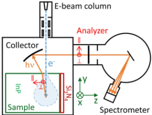
Cathodoluminescence spectroscopy imaging is performed on a Rosa instrument from Attolight (Fig. 2without the “Analyzer”). In this tool, a focused electron beam scans the sample with nor-mal incidence while the optical emission is collected. After exit-ing the vacuum chamber, the optical beam is analyzed by usexit-ing a spectrometer to obtain a luminescence spectrum for each pixel of the image. The spectrometer consists of a 32 cm monochroma-tor from Horiba Jobin Yvon fitted with a 1024 × 1024 EMCDD high-speed camera adapted for UV-visible detection (200-1100 nm). The camera enables near-instant acquisition of the entire emission spectrum.
In all experiments, the sample is measured in a cross-sectional view at room temperature. The current and voltage of the incident e-beam are set to 4 nA and 5 kV, respectively. The scans are square and their size varies from 5 to 42 µm, depending on the width of the mea-sured line on the sample, while the number of data points is kept at 128 × 128. The integration time at each pixel is set to 10 ms, resulting in a total acquisition time for one image of 168 s. The monochroma-tor entrance slit is adjusted from 300 to 900 µm, depending on the image size, to avoid shadowing the optical beam while scanning.
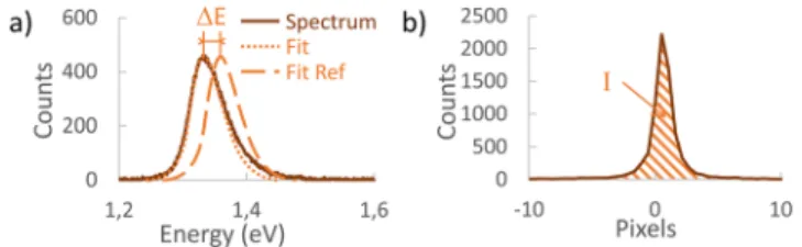
Acquired luminescence spectra result from electronic transi-tions around InP’s bandgap.40 After acquisition, the spectrum at each pixel is approximatively fitted with a Gaussian curve [Fig. 3(a)]. A peak energy is determined from the Gaussian center. A peak shift is obtained by subtracting from the peak energy a reference value measured far from features, in practice close to the middle of the cross section. The reference value is an average over the entire reference image. If we assume that the measured peak energy corresponds to the difference between the conduction band and a weighted valence band average, the peak shift ∆E is proportional to the hydrostatic strain εh21,22
∆E = a × εh, with a = −6.6 eV for InP. (1)
Review of
Scientific Instruments
ARTICLE scitation.org/journal/rsiFIG. 3. Basic data treatment at each image pixel. Determination of (a) the energy
shift∆E from 1st order spectroscopic acquisitions at the pixel of interest and on a reference and (b) the intensity I from 0 order acquisition. The energy shift is used for hydrostatic strain determination. Zero order intensities of orthogonally polarized emissions are used for strain anisotropy determination, via the calculation of the DOP.
A positive ∆E corresponds to a hydrostatic compression, whereas a negative one corresponds to a hydrostatic extension.
2. DOP measurements
The DOP measurement technique using CL is similar in prin-ciple to that using PL.4,19,26–31The DOP of the emitted light is given by
DOP =I− I∥ I+ I∥
, (2)
where I and I∥ are the intensities of light whose polarization are, respectively, perpendicular to and within the plane of the schematic inFig. 2. In order to measure I and I∥, the tool is modified by adding a WB25M-UB wire grid polarizer from Thorlabs (“Analyzer” inFig. 2) between the collector and the spectrometer. The values I and I∥are then measured with the analyzer in the vertical and horizontal positions (Fig. 2), respectively. In our current implemen-tation, separate I and I∥ images are acquired, the analyzer being rotated manually between the two positions. A spectrometer is not needed for measuring the total emission intensity of a bulk mate-rial. A photodiode placed right after the analyzer would do as well. However, the spectrometer cannot be removed because of other tool usages, which leaves two options: integrating the (1st order) emission spectrum over energies or adding the intensities of all the camera pixels of the reflected (0-order) signal [Fig. 3(b)]. In order to increase the signal to noise ratio, we chose a 0-order acquisition with the entrance slit of the monochromator wide open. The lim-ited number of illuminated pixels on the camera, ∼40 when taking the two dimensions into account [Fig. 3(b)], did not prove to be a problem. However, this could be improved by slightly defocusing the optical collection. Also, replacing the grating in the monochromator with a mirror would further increase the signal.
During measurements, the cross-sectioned surface of the sam-ple is placed facing the e-beam inFig. 2. In this configuration, the direction, or s polarization of the light beam exiting the sample, corresponds to the x direction on the sample. The ∥ direction, or p polarization of the light beam exiting the sample, depends on the direction of the emitted beam. However, because of the high opti-cal index of InP, only small solid angles emitted within the material are collected, and we will assume, as a first approximation, that the ∥ direction is the z direction of the sample. Aside from the
spectrometer settings and the integration time (see Sec. II C 3), the tool settings are the same as for spectroscopic measurements.
The DOP is proportional to strain anisotropy within the mea-sured plane28
DOP = −C × (ε− ε∥), (3)
where εand ε∥are the material strains in the , or x, and ∥, or z, directions, respectively, inFig. 2. The coefficient C has been deter-mined to be 65 for InP.29Spectrometric and DOP measurements provide complementary information on the deformation matrix. The shift in energy of the emission does not provide information on the direction of the deformation. DOP measurement gives the difference between deformations in the plane orthogonal to the collection.
C. Preliminary DOP studies
Before DOP measurements are made on strained samples, two feasibility studies are carried out on the following potential issues: the polarization transmission through the optical collection system and the stability of the emitted intensity.
1. Polarization transmission through the optical collection system
Optical fibers are known to scramble light polarization. For that reason, the absence of a fiber optic cable between the collector and the spectrometer in the design of the Attolight tool encouraged us to attempt measuring the DOP of the emitted luminescence. However, the series of mirrors composing the optical collector may also alter polarization.
We consequently started our study by investigating the polar-ization transmission through the optical collection system. For that purpose, a source of polarized light is placed on the sample stage in the CL equipment (Fig. 2) with the direction of polarization first in the direction and then in the ∥ direction. In both cases, the ana-lyzer angle θ is rotated in steps of 10○
starting from the ∥ position.
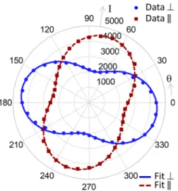
Figure 4presents polar plots of the total intensity (I) measured after the analyzer and the monochromator, set at 0 order. The two sets of data are fitted using a modified Malus’ law
I = Iunpolarized+ Ipolarized× cos(θ − θrot), (4) where Iunpolarized is the intensity of unpolarized light and θrot an angular shift from the horizontal position. It appears that the trans-mitted optical beams are roughly half polarized and the polarization is rotated by 10○.Figure 4also illustrates a difference between the maximum intensities collected from the and the ∥ polarizations at the sample. This is evident when comparing the intensities at 80○
for the polarization and at −10○for the ∥ polarization.
The observed polarization rotation θrotcan be due to various optical misalignments, including that of the analyzer. To compen-sate for it, from now on, Iand I∥will be measured with the analyzer rotated by 10○from the horizontal or vertical position. The observed polarization loss is due to the collecting mirrors and to the spectrom-eter grating. In order to differentiate between the two contributions, the polarization loss due to the spectrometer grating was evaluated separately. It varies from 64% to 83% depending on the polarization direction of the incident beam. The polarization transmission from the collection mirrors is deducted to vary from 72% to 65%. The design of the collecting mirrors is constrained by the electron gun
Rev. Sci. Instrum. 90, 043701 (2019); doi: 10.1063/1.5078506 90, 043701-3
FIG. 4. Polar plots of intensities (I) transmitted through the optical collector and
the monochromator.θ is the analyzer angle from the horizontal position. Data are displayed as round and square markers for the transmission of and ∥ polarized light at the stage, respectively. Plain lines represent a fit using a modified Malus’ law that includes unpolarized light and a rotation.
and difficult to change. To reduce the grating’s impact, one could replace it with a mirror or add a quarter-wave plate between the analyzer and the spectrometer.
A more thorough characterization of the transmission of polar-ization through the optical collector, as done by Osorio et al.34on their system, would be useful. Here, we simply compensated for the transmission difference between the and ∥ polarizated light by adding a correction factor to the DOP calculation, which becomes
DOP = I ∝− I∥ I α + I∥ , (5)
where α is the total ratio between the transmissions of and ∥ polar-izations including the optical collector and the monochromator’s grating.
2. Stability of the emitted intensity
The calculation of DOP images from Eq.(2)requires two CL intensity images acquired from the same sample area tens of seconds apart. Potential issues include stage drift and the effect of sample charging on the emitted light intensity.Figure 5demonstrates that, contrary to the peak energy, the luminesced intensity varies greatly with time during the first 14 min of imaging. A sample charging time of 10-15 min is thus waited before capturing the first image, arbitrar-ily of the polarized intensity. In addition, relative to spectroscopic measurements, the time per image is reduced to 64 s by reducing the integration time per pixel from 10 to 5 ms; this also limits the effect of spatial drift. Furthermore, two images of the polarized intensity are taken, one before that of the ∥ polarized intensity and one after; the two images are geometrically averaged before DOP calculation using Eq.(5). In Cassidy’s PL tool,29although sample charging is not an issue, a rotating polarizer enables simultaneous acquisition of Iand I∥, thus avoiding drift issues.
FIG. 5. Evolution of the luminescence intensity with measurement time for three
e-beam settings. Intensities are normalized.
As illustrated inFig. 5, after normalization, the evolution of the emitted intensity with time is mostly independent of e-beam settings and cannot be used for selecting the best conditions. Nonetheless, the unnormalized value of the emitted intensity decreases greatly when reducing the voltage or current; therefore, the noise on the DOP increases. To the contrary, the size of the pear-shaped inter-action volume of the e-beam with the material increases with the voltage, thus reducing the lateral resolution. An e-beam voltage of 5 kV and an e-beam current of 4 nA are a good compromise, as for spectrometric measurements. Despite the variation of emitted light intensity, the DOP does not depend on e-beam parameters within the range of values tested.
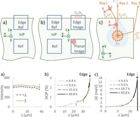
D. Corrections from references 1. DOP measurements
In order to evaluate our method and to compensate for eventual parasitic effects on processed samples, a bare InP sample is measured in two different areas of a cleaved cross section [Fig. 6(a)]: far from edges (“Ref”) and on the edge (“Edge Ref”). Far from edges, despite the absence of strain, the intensities of light emitted with and ∥ polarizations are slightly different [Fig. 7(a)], which would lead to a non-zero DOP using Eq.(2). In Sec.II C 1, when the sample was replaced by a polarized light source, the difference was mainly due to the polarization dependence of the spectrometer grating reflectance. Here, other potential sources of difference are the different trans-mission coefficients of the (s) and ∥ (p) polarizations of the light exiting the sample at its top surface [Fig. 6(c)] for non-zero inci-dent angles [“Ray 1” inFig. 6(c)], as described by Fresnel’s equations. For a planar sample far from edges, this effect is largely canceled by the symmetry of the system, but it may still account for part of the observed difference.Figure 7(b)illustrates the DOP measured on the edge of the cleaved cross section [“Edge Ref” onFig. 6(a)] of a bulk sample as calculated from Eq.(5)with α computed from the “Ref” image far from edges. As expected from the correction, far from the edge (at z = 0 µm), the DOP is null. Closer to the edge, however, the DOP increases. The main origin of this increase is the collection of light exiting the sample from its side [“Ray 3” inFig. 6(c)]. In this case, the difference in transmittance of the (s) and ∥ (p) polar-ized components of the emitted light is not compensated for by the system’s symmetry or by the correction [Eq.(5)] based on a flat ref-erence sample. Other physical phenomena due to the presence of an additional surface are possible.
Review of
Scientific Instruments
ARTICLE scitation.org/journal/rsiFIG. 6. Position of the measurements on (a) a bulk cleaved
sample and (b) the “patterned HM” sample. The “Planar Image” in (b) is a hypothetical measurement. (c) Refraction at the sample’s surface of a selection of emitted light rays. “Ray 1” and “Ray 2” cross the top surface. When measuring close to an edge, rays such as “Ray 3” can also cross the side surface and reach the optical collector. For a normal incidence (“Ray 2”), the transmittance (T) is the same for all polarizations. For other incidences, T∥>T.
FIG. 7. Measurements on the cleaved cross section of a
bulk InP reference sample. (a) Measurements of and ∥ polarized intensities far from edges at a 4.4 k magnification. (b) and (c) Measurements on the edge at magnifications from 4.4 k to 69.8 k of (b) DOP and (c) energy shift (∆E). Images are averaged along the x direction to obtain a profile of the variation with z.
For a measurement on processed features far from the edges of a planar sample [hypothetical “Planar Image” onFig. 6(b)], the difference between the total transmission of the and ∥ compo-nents of light emitted within the sample can be compensated for by using Eq.(5)with a ratio α measured on the same sample far from edges and features [“Ref” inFig. 6(b)] using the same parameters. In practice, α is about 0.91, as can be observed inFig. 7(a). For a mea-surement on processed features at the sample’s edge, for instance on the cross section of the “patterned HM” sample [“Edge Image” in
Fig. 6(b)], an average profile, such as the one shown inFig. 7(b), also taken on the edge but sufficiently far from features [“Edge Ref” inFig. 6(b)] is subtracted line by line from the raw measure-ment to suppress edge effects. For the “etched” sample [Fig. 1(b)], the complex geometry prevents a straightforward compensation for edge effects and only the differential transmission of polarization is compensated for by using Eq.(5).
2. Spectroscopy measurements
Spectroscopy measurements of the “patterned HM” and “etched” samples (Fig. 1) are corrected similarly to DOP measure-ments. In this case, the average peak energy of an image measured far from the sample’s edge [“Ref” inFig. 6(b)] serves as the reference for energy shift determination as already mentioned in Sec.II B 1. An edge effect is also observed on the energy shift emitted from a cleaved bulk sample; as shown inFig. 7(b), the energy increases close to edges. The origin of this effect is unclear, but it is material depen-dent. It is dealt with in the same way as for DOP measurements (see above). In addition, on all images of all samples, a constant slope along the x axis is subtracted. This small slope on ∆E vs x is due to variations in the path of light rays as the e-beam scans the sample. There is no such slope on ∆E vs z as path changes are parallel to the monochromator’s slit and the CCD signal is summed vertically.
III. MEASUREMENTS A. Patterned HM samples
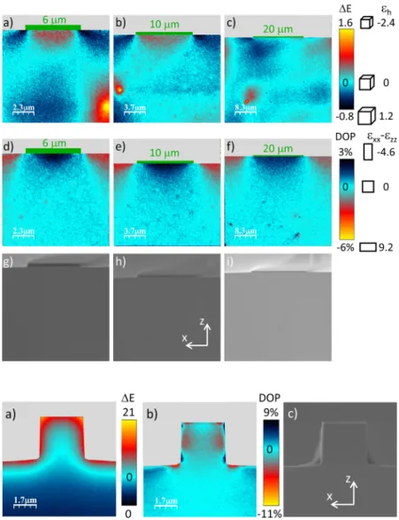
Figure 8presents images measured by CL on “patterned HM” samples [Fig. 1(a)]. Samples with 6, 10, and 20 µm wide Si3N4 HM stripes are presented. Energy shift (∆E) images are shown in
Figs. 8(a)–8(c). Images for 6 and 10 µm HM stripes [Figs. 8(a)and
8(b)] are of good quality. The observed compressed area under the HM and the two symmetric lobes of extended material on each side are characteristics. They are also predicted by simulations, either by a simple edge force model or by finite element analysis (FEM).19 As expected, the sensitivity to strain of CL spectroscopy is excellent. However, the bright features observed at several places far under the HM show that it is also very sensitive to other physical properties of the material. These features are not present in the secondary elec-tron images acquired simultaneously [Figs. 8(g)and8(h)] and may be attributed to impurities or lattice defects. The presence of such features in apparently random areas of the image affects the data treatment, which may explain the poor quality ofFig. 8(c)taken on the sample with a 20 µm wide HM. DOP images taken at the same place as ∆E images are shown inFigs. 8(d)–8(f). Although the information provided is different, a compressed area under the HM and extended areas on each side are also observed. The sensitivity to strain of this new technique is observed to be as good as that of CL spectroscopy and the DOP of PL20or about 10−5. In addition, compared to CL spectroscopy, it is less sensitive to impurities or lat-tice defects; DOP images are exempt of the bright features observed on spectroscopic images, and the quality of the image inFig. 8(f)is as good as the other two. For very thin layers, the DOP is however sensitive to film thickness due to a quantum effect.27The lateral res-olution is the same as that of CL spectroscopy and much improved compared to the DOP of PL,20which enables the imaging of smaller
Rev. Sci. Instrum. 90, 043701 (2019); doi: 10.1063/1.5078506 90, 043701-5
FIG. 8. Images measured on cleaved cross sections of InP
samples strained by thin stripes of patterned Si3N4hard
masks of three different widths: (a), (d), and (g) 6µm; (b), (e), and (h) 10µm; and (c), (f), and (i) 20 µm. (a), (b), and (c) Energy shift (∆E) measured by CL spectroscopy. (d), (e), and (f) Degree of polarization (DOP) of the luminescence. (g), (h), and (i) Secondary electron images. For each HM width, the three types of images are taken at the exact same place.∆E is in meV. Calculated strains (εhandεxx-εzz) have
to be multiplied by 10−4.
FIG. 9. (a) Energy shift (∆E), (b) degree of polarization
(DOP), and (c) secondary electron measurements on the cross section of 3µm wide patterns etched in a bulk InP sample. The three images are acquired from the same area. ∆E is in meV.
samples such as the one with a 6 µm HM. Because light is collected over a large area, lateral resolution is limited by two physical effects: the size of the pear-shaped e-beam interaction volume and carrier diffusion. To give an idea of the pear size, for an accelerating volt-age of 5 kV, the depth below the surface for maximum electron-hole pair generation is about 100 nm.41The presence of minority carri-ers decays around their point of generation according to the rules of diffusion.23All together, the resolution is a few hundred nanome-ters with a large field of view. ∆E and DOP measurements provide complementary information on the strain: εh= εxx+ εyy+ εzzand εxx− εzz. It is consequently interesting to measure them on the exact same area of the sample.
B. Etched samples
Figure 9 displays CL measurements on the cross section of 3 µm wide patterns etched in bulk InP [Fig. 1(b)]. These measure-ments emphasize the high resolution of the technique. However, they are not corrected for the edge effects observed on a bulk cleaved
sample [Figs. 7(b)and7(c)]. The ∆E image inFig. 9(a)is dominated by the edge effect seen inFig. 7(c). The main features observed close to edges on the DOP image [Fig. 9(b)] are also most likely due to the subtler edge effect ofFig. 7(b). As expected, the effect is oppo-site for edges at 90○from each other. Nonetheless, the features close to corners can be attributed to strain. For both ∆E and DOP, an edge effect compensation, via hardware or software, would be nec-essary to extract accurate strain information on samples of complex shape.
IV. CONCLUSION
A new strain measurement technique based on the DOP of CL has been developed and tested on InP samples strained by a thin patterned hard mask. As expected, its strain sensitivity is excellent at 10−5, which is comparable to that of CL spectroscopy and the DOP of PL and better than that of µ-Raman and SEM- or TEM-based elec-tron diffraction techniques. The DOP of CL is less sensitive to defects
Review of
Scientific Instruments
ARTICLE scitation.org/journal/rsithan CL spectroscopy and has a higher lateral resolution than the DOP of PL. The lateral resolution, a few hundred nanometers, is also better than that of µ-Raman and slightly better than that of ESBD and TEM-based techniques. Its field of view is easily adjustable, up to several tens of microns, by changing magnification, as that of µ-Raman and ESBD but contrary to TEM. Sample preparation is the same as for µ-Raman and ESBD and simpler than for TEM. Strain results are less affected by the preparation than those obtained by TEM. Spectroscopic and DOP images can be acquired at the exact same place providing complementary data on strain. Spectroscopic and DOP measurements on strained InP are consistent and agree with previous data and simulations.
ACKNOWLEDGMENTS
This work has been supported by the LabEx Minos No. ANR-10-LABX-55-01, the RENATECH program, and the IRT Nanoelec No. ANR-10-AIRT-05. This work made use of the nanocharacteri-zation platform (PFNC) facilities at Minatec.
REFERENCES
1
M. L. Lee, E. A. Fitzgerald, M. T. Bulsara, M. T. Currie, and A. Lochtefeld,J. Appl. Phys.97, 011101 (2005).
2C. S. Adams and D. T. Cassidy,J. Appl. Phys.64, 6631 (1988). 3N. K. Dutta and D. C. Craft,J. Appl. Phys.56, 65 (1984).
4D. Lisak, D. T. Cassidy, and A. H. Moore,IEEE Trans. Compon., Packag., Manuf.
Technol., Part A24, 92 (2001).
5
L. S. Yu, Z. F. Guan, W. Xia, Q. Z. Liu, F. Deng, S. A. Pappert, P. K. L. Yu, S. S. Lau, L. T. Florez, and J. P. Harbison,Appl. Phys. Lett.62, 2944 (1993).
6I. C. Bassignana, C. J. Miner, and N. Puetz,J. Appl. Phys.65, 4299 (1989). 7V. S. Harutyunyan, A. P. Aivazyan, E. R. Weber, Y. Kim, Y. Park, and S. G.
Subramanya,J. Phys. D: Appl. Phys.34, A35 (2001).
8
D. Rouchon, M. Mermoux, F. Bertin, and J. M. Hartmann,J. Cryst. Growth392, 66 (2014).
9J. Li, D. Anjum, R. Hull, G. Xia, and J. L. Hoyt,Appl. Phys. Lett.87, 222111
(2005).
10
P. Zhang, A. A. Istratov, and E. R. Weber,Appl. Phys. Lett.89, 161907 (2006).
11
A. J. Wilkinson and T. B. Britton,Mater. Today15, 366 (2012).
12
M. Hanke, M. Dubslaff, M. Schmidbauer, T. Boeck, S. Schöder, M. Burghammer, C. Riekel, J. Patommel, and C. G. Schroer,Appl. Phys. Lett.92, 193109 (2008).
13
M. Hÿtch, F. Houdellier, F. Hüe, and E. Snoeck,Nature453, 1086 (2008).
14
M. Gal, P. J. Orders, B. F. Usher, M. J. Joyce, and J. Tann,Appl. Phys. Lett.53, 113 (1988).
15
M. Grundmann, J. Christen, F. Heinrichsdorff, A. Krost, and D. Bimberg, J. Electron. Mater.23, 201 (1994).
16
H. Xue, N. Pan, M. Li, Y. Wu, X. Wang, and J. G. Ho,Nanotechnology21, 215701 (2010).
17
M. Avella, J. Jiménez, F. Pommereau, J. P. Landesman, and A. Rhallabi,Appl. Phys. Lett.93, 131913 (2008).
18
R. Chanson, A. Martin, M. Avella, J. Jiménez, F. Pommereau, J. P. Landesman, and A. Rhallabi,J. Electron. Mater.39, 688 (2010).
19
J.-P. Landesman, D. T. Cassidy, M. Fouchier, E. Pargon, C. Levallois, M. Mokhtari, J. Jimenez, and A. Torres,J. Electron. Mater.47, 4964 (2018).
20
J.-P. Landesman, D. T. Cassidy, M. Fouchier, C. Levallois, E. Pargon, N. Rochat, M. Mokhtari, J. Jiménez, and A. Torres,Opt. Lett.43, 3505 (2018).
21
S. C. Jain, M. Willander, and H. Maes,Semicond. Sci. Technol.11, 641 (1996).
22
I. Vurgaftman, J. R. Meyer, and L. R. Ram-Mohan,J. Appl. Phys.89, 5815–5875 (2001).
23
Y. Rosenwaks, Y. Shapira, and D. Huppert,Phys. Rev. B45, 9108–9119 (1992).
24
Y. Tang, D. H. Rich, E. H. Lingunis, and N. M. Haegel,J. Appl. Phys.76, 3032 (1994).
25F. H. Peters and D. T. Cassidy,Appl. Opt.
28, 3744 (1989).
26P. D. Colbourne and D. T. Cassidy,IEEE J. Quantum Electron.
29, 62 (1993).
27B. Lakshmi, D. T. Cassidy, and B. J. Robinson,J. Appl. Phys.
79, 7640 (1996).
28B. Lakshmi, B. J. Robinson, D. T. Cassidy, and D. A. Thompson,J. Appl. Phys.
81, 3616 (1997).
29
D. T. Cassidy,Mater. Sci. Eng., B91-92, 2 (2002).
30
D. T. Cassidy, S. K. K. Lam, B. Lakshmi, and D. M. Bruce,Appl. Opt.43, 1811 (2004).
31D. T. Cassidy, C. K. Hall, O. Rehioui, and L. Bechou,Microelectron. Reliab.
50, 462–466 (2010).
32
N. Yamamoto, S. Bhunia, and Y. Watanabe,Appl. Phys. Lett.88, 153106 (2006).
33
B. J. M. Brenny, D. van Dam, C. I. Osorio, J. Gómez Rivas, and A. Polman,Appl. Phys. Lett.107, 201110 (2015).
34C. I. Osorio, T. Coenen, B. J. M. Brenny, A. Polman, and A. F. Koenderink,ACS
Photonics3, 147 (2016).
35
V. Myroshnychenko, N. Nishio, F. J. García de Abajo, J. Förstner, and N. Yamamoto,ACS Nano12, 8436 (2018).
36V. L. Alperovich, A. S. Terekhov, A. S. Jaroshevich, G. Lampel, Y. Lassailly,
J. Peretti, N. Rougemaille, and T. Wirth,Nucl. Instrum. Methods Phys. Res., Sect. A536, 302 (2005).
37J. J. G. M. van der Tol, Y. S. Oei, U. Khalique, R. Nötzel, and M. K. Smit,Prog.
Quantum Electron.34, 135 (2010).
38
G.-H. Duan, C. Jany, A. Le Liepvre, A. Accard, M. Lamponi, D. Make, P. Kaspar, G. Levaufre, N. Girard, F. Lelarge, J.-M. Fedeli, A. Descos, B. Ben Bakir, S. Messaoudene, D. Bordel, S. Menezo, G. de Valicourt, S. Keyvaninia, G. Roelkens, D. Van Thourhout, D. J. Thomson, F. Y. Gardes, and G. T. Reed, IEEE J. Sel. Top. Quantum Electron.20, 158 (2014).
39
G. Crosnier, A. Bazin, V. Ardizzone, P. Monnier, R. Raj, and F. Raineri,Opt. Express23, 27953 (2015).
40I. Tsimberova, Y. Rosenwaks, and M. Molotskii, J. Appl. Phys.
93, 9797 (2003).
41
J.-M. Bonard, J.-D. Ganière, B. Akamatsu, D. Araújo, and F.-K. Reinhart, J. Appl. Phys.79, 8693 (1996).
Rev. Sci. Instrum. 90, 043701 (2019); doi: 10.1063/1.5078506 90, 043701-7