© 2019 ISTE OpenScience – Published by ISTE Science Publishing, London, UK – openscience.fr Page | 1
g
m
/I
D
based methodology for capacitive feedback LNA
design
Méthodologie basée sur g
m/ I
Dpour la conception de LNA à retour
capacitifs
Jing Liu1, Estelle Lauga-Larroze1, Serge Subias1, Frédéric Hameau2, Jean-Michel Fournier1, Carlos Galup3, Sylvain Bourdel1
1
RFIC-Lab, Univ. Grenoble Alpes, Grenoble INP, France, estelle.lauga-larroze@univ-grenoble-alpes.fr
2
CEA LETI, France
3
Universidade Federal de Santa Catarina, Brazil
ABSTRACT. A gm/ID based methodology is detailed in this paper in order to help the designers to determine the optimum
size of a capacitive feedback LNA by considering the design topology, the specifications to reach and the technology characteristics. Thanks to this methodology, the gm/ID is maximized to minimize the power consumption under design
constraints which are the voltage gain, the NF and the input inductor (input Q-factor set). To illustrate this methodology, some capacitve feedback LNAs have been designed with different voltage gain requirements in 28nm FDSOI technology for 2.4GHz applications. Based on the initial parameters obtained following the different steps, three LNAs have been designed and simulated. The post-layout simulation results exhibit very good performances in terms of power consumption, linearity IIP3, bandwith BW and noise figure NF for the three given voltage gains (15dB, 18dB and 20dB). The achieved performances are quantified by high values of a well known FoM.
KEYWORDS. gm/ID approach, design methodology, capacitive feedback LNAs.
1. Introduction
With advanced technologies, the way of designing RF circuits is changing. In early nineties the need for low cost RF system dedicated to consumer market such as GSM pushed the RF domain in the CMOS bulk area. At this time, the ft of the technologies was low and reaching a RF bandwidth of few gigahertzes was one of the
major issues. As a result, most of RF circuits were designed in the strong inversion where the MOS transistor achieves the best ft. As a consequence, numerous design method were developed based on Active/Triode region
model valid for Vgs>Vth[Vinaya 15].
However, for RF design, the paradigm is changing since advanced technologies perform very well in terms of ft [Shameli 06]. For consumer market such as 5G and IoT, and thanks to advanced technologies, the issue is
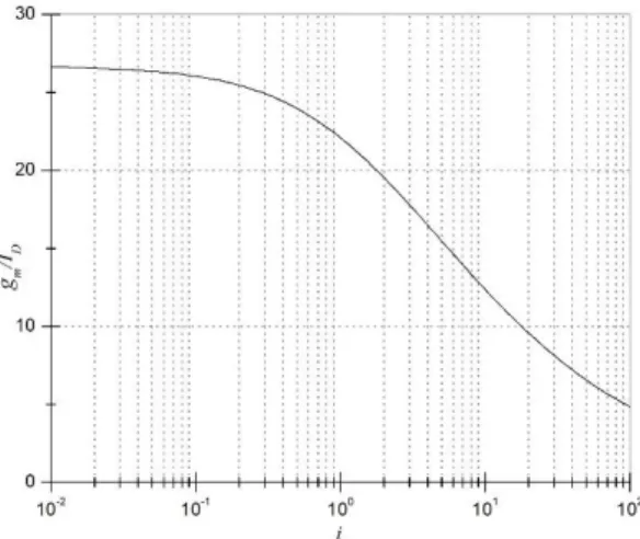
moving from the bandwidth to the power consumption since the demand is high to increase the number of services in the same mobile terminal or to provide long life communication nodes. As a consequence, the trend is to design circuit in subthreshold regions [Song 08] [Fadhuile 14]. Indeed, as presented in Figure 1, the efficiency of the device, which can be characterized by gm/ID increases as the inversion level of the channel
reduces. Following this trend, several works study the optimal region of operation by considering a given function and a given technology. In [Shameli 06], a FOM based on gm ft /ID is introduced which allows to
maximize the efficiency bandwidth product in the design of RFIC. In [Song 08], a FOM dedicated to Low Noise Amplifier (LAN) and based on gm2/ID is introduced to take into consideration the NF whereas the authors in
[Fadhuile 14] proposed a slightly modified FOM to add the ft. All these approaches help the designers to choose
the region of operation by considering functionalities and a technology but do not take into account the topologies and the specifications. Optimizing such FOM could lead to oversize the circuits in term of bandwidth or consumption for example.
© 2019 ISTE OpenScience – Published by ISTE Science Publishing, London, UK – openscience.fr Page | 2
In the nineties, gm/ID based methodologies have been proposed to optimize the power efficiency of several
circuits such as OTA [Silveira 96]. These approaches are generally dedicated to a particular topology and allow the sizing of the transistors in all region of operation to reach given performances. To do so, the designer uses a set of equations which describe the performances of the topology and which help him determining the gm/ID
needed to reach requirements. Then, based on abacus which gives the gm/ID as function of the transistor size, the
topology can be sized for a given current. At this time, abacus was needed since all region models such EKV
[Enz 95] or ACM [Galup 07] were not widespread. These general approaches have been used for several topologies and to optimize different performances in low frequency domain but are still quite unused in RF.
The objective of this article is to present gm/ID based methodologies for the design of a Capacitive Feedback
LNA (CF-LNA). A method which follows the same general approach than the one presented in [Silveira 96] is given. With this method, the gm/ID is maximized to minimize the power consumption under design constraints
which are the Gain, the NF and the input inductor which set the circuit size.
Figure 1. gm/ID versus if in FDSOI 28nm 2. CF-LNA Topology
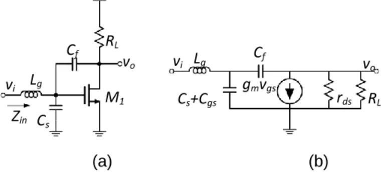
The topology of the considered CF-LNA is given in Figure 2. The small signal gain is derived in annex and can be approximated by:
. o L ds V m O m gs L ds v R r A g R g v R r [1]
with RO=rds//RL . AV can be expressed in terms of the Early voltage as follow:
DD DS
A DS
m V D DD A V V V V g A I V V [2]Av depends on the region of operation through the ratio gm/ID. For low values of VA (i.e. VDD>>VA) as it is the
case in advanced technologies, AV is maximum for VDSOPT=(VDD-VA)/2. The maximum gain AV_max is then
reached for: 2 DD A ds L D V V r R I [3]
and is equal to:
_ max . 4 m DD A m V EOPT D D g V V g A V I I [4]
© 2019 ISTE OpenScience – Published by ISTE Science Publishing, London, UK – openscience.fr Page | 3 . 4 DD A EOPT O D V V V R I [5]
Otherwise, for non-advanced technologies, i.e. VDD<<VA, RL must be maximized to maximize the gain.
When designing a LNA, it is first mandatory to match the input impedance to the 50 Ω antenna. As shown in annex, adding Cf feedback helps to synthesize a real part in the input impedance. An inductor is also needed to
null the imaginary part and achieve the power matching. In addition, a capacitor Cs is used to add flexibility in
the sizing as it will further be developed.
(a) (b)
Figure 2.Capacitive Feedback LNA structure (a) and its small signal model (b)
In LNA design, the NF is another requirement that must be controlled trough the design. The NF is mainly related to the gm of the MOS as follow:
2 1 1 m g m g O NF g R g R R [6]
We can notice that the NF depends little on the operation region since varies little with Vgs. The gain, the
matching and the NF are the main requirements when designing LNA. However, other requirements can arise depending on the application like the size or the bandwidth.
3.Method for Area Reduction
The purpose of this method is to fulfill Gain and NF requirements with the smallest possible consumption while controlling the value of the Lg to limit the area of the circuit.
From [1] and [22] it is possible to express the LNA’s gain as follow:
2 . 1 L ds LNA m p L ds R r A g Q R r [7]
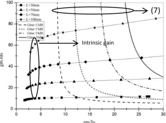
which leads to Eq. [8] of the intrinsic gain (gm.rds) as a function of gm/ID and ALNA_max obtained for VDSOPT:
2 2 _ max 1 1 1 1 1 2 P P m m ds LNA m L LNA EOPT D Q Q g g r A g R A V I [8]
[8] is plotted for several values of gain on Figure 3 for a given value of Qp which allows the choice of Lg.
To obtain the optimal operating point, the intrinsic gain gm.rds of different transistors is plotted on the same
abacus (Figure 3). Lg Cf RL M1 Zin vi vo Cf RL vo Lg vi Cs+Cgs gmvgs rds Cs
© 2019 ISTE OpenScience – Published by ISTE Science Publishing, London, UK – openscience.fr Page | 4 Figure 3. gm.rds vs gm/ID for Qp =1
It is then possible to choose a value of gm/ID which is maximum for a required gain which finally maximizes
the efficiency of the circuit.
The value of gm is then chosen regarding the NF given by [6]. In first order approximation, NF does not
depend on L neither on gm/ID. Then, the value of gm/ID, gm and ID are determined (for a given NF and GV). W/L
is extracted from the abacus which give ID/W/L(gm/ID) presented on Figure 4 and RO and rds are determined with
[2]. As presented in equation [14] and [15], Re(Zin) and Im(Zin) only depend, at this step, on Cs and Cf which
are set to have simultaneously Re(Zin)=50 and Im(Zin)=0.
Figure 4. ID/(W/L) vs gm/ID
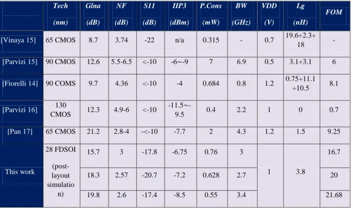
This method has been used to design LNAs with different voltage gain requirements in 28nm FDSOI technology for 2.4GHz applications. Results are summarized in theTable 1:
Glna (dB) NF (dB) gm (mS) gm/ID ( ) L (nm) ID (mA) R0 (Ω) W (µm) 15 <3 15 21 30 0.714 560 83 18 14 22 50 0.636 943 53 20 12 23 70 0.522 1149 54
Table 1. LNA sizing to reach three different gain values
(7)
© 2019 ISTE OpenScience – Published by ISTE Science Publishing, London, UK – openscience.fr Page | 5
In the proposed method, Vea is supposed constant. However, it varies with L and gm/ID. To limit iteration in
the method, the value of Vea must be corrected as soon as the operating point is known.
4. Results
These three LNAs have been designed based on these initial parameters and considering a quality factor Qp
set to 1. Input matching is reach by adding Cf and Cs. A slight tuning has been done by simulation to refine the
results. The simulation results concerning the 15dB gain LNA are shown in Figure 5. At 2.4GHz, the voltage gain of LNA reaches 15.7dB while NF is equal to 3dB. The IIP3 linearity is -6dBm. The LNA consumption is 760µW under 1V of power supply.
Figure 5. Voltage gain, input matching and NF simulated results of the 15dB gain LNA
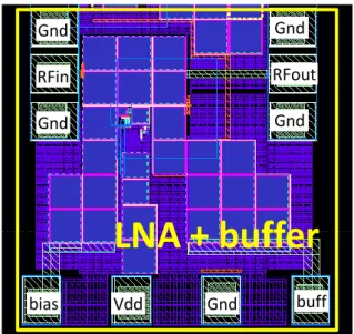
To validate this approach, these LNAs have been designed. For measurement convenience, a matching buffer has been added at the output of the LNAs to ensure the output matching of the circuit. The silicon area occupied by this circuit (LNA + buffer) is 127µm x 170µm without pads, 400µm x 378µm with pads as illustrated in Figure 6.
Figure 6.Layout of the LNA with a 15dB voltage gain
The post-layout simulation results are given in Table 2. Overall performances of LNAs are compared with the following FoM:
Gnd Gnd RFin Gnd Gnd RFout Gnd Vdd bias buff
LNA + buffer
© 2019 ISTE OpenScience – Published by ISTE Science Publishing, London, UK – openscience.fr Page | 6
. 10 . 3 20 log 1 V av lin GHz mW dc mW av lin G BW IIP FoM P F [9] Tech (nm) Glna (dB) NF (dB) S11 (dB) IIP3 (dBm) P.Cons (mW) BW (GHz) VDD (V) Lg (nH) FOM[Vinaya 15] 65 CMOS 8.7 3.74 -22 n/a 0.315 - 0.7 19.6+2.3+
18 - [Parvizi 15] 90 CMOS 12.6 5.5-6.5 <-10 -6 -9 7 6.9 0.5 3.1+3.1 6 [Fiorelli 14] 90 COMS 9.7 4.36 <-10 -4 0.684 0.8 1.2 0.75+11.1 +10.5 8.1 [Parvizi 16] 130 CMOS 12.3 4.9-6 <-10 11.5 -9.5 0.4 2.2 1 0 0.7 [Pan 17] 65 CMOS 21.2 2.8-4 -<-10 -7.7 2 4.3 1.2 1.5 9.25 This work 28 FDSOI (post-layout simulatio n) 15.7 3 -17.8 -6.75 0.76 3 1 3.8 16.7 18.3 2.57 -20.7 -7.2 0.628 2.7 20 19.8 2.6 -17.4 -8.5 0.55 3.4 21.68
Table 2. Comparison performances of LNAs
The simulated results of this capacitive feedback LNAs are compared in Table 2 with other circuits realized
and measured in the same framework. Even if this comparison is not exhaustive since only simulations are presented here, the proposed design approach seems to be attractive since the resulting FoM is very good. We especially show that gain between 15 to 20dB with NF lower than 3dB can be expected with power consumption of 0.55 to 0.76mW and with a sufficient bandwidth to address RF applications if the gm/ID is
maximised.
5. Conclusion
Based on the gm/ID approach, a detailed methodology allowing the design of capacitive feedback LNAs is
presented step by step. To illustrate it, some CF-LNA designs have been realized in 28nm FDSOI technology to reach a given Gv and NF at minimum power consumption for 2.4GHz applications. The post-layout simulation results show good RF performances highlighted by the FOM results. The presented methodology aims to help designers to adopt the gm/ID approach which is perfectly suited to determine the optimum sizes in terms of
consumption for given values of specifications. Furthermore, the gm/ID approach appears to be well suited for
advanced technologies for which the ft is very high.
Acknowledgement: This work has been granted by the European program ECSEL through the project
OCEAN12.
6.Annexes
In this annex, the main equations of the CF-LNA proposed in Figure 2 are derived. The input impedance of the structure is given by
1 1 / / IN g M g IN gs IN Z L p Z L s R C p C p [10]
© 2019 ISTE OpenScience – Published by ISTE Science Publishing, London, UK – openscience.fr Page | 7
with Lg the input inductance, Cgs the input parasitic capacitances of the transistor M1, and ZM the Miller
impedance due to the capacitive feedback which can be expressed as follow if and the output capacitance CO is much lower than Cf:
[11]
1 ( ) O f m o v m O gs O f O R C p g v A g R v R C C p [12]with RO=rds//RL . With ZM, it is possible to express the real part and the imaginary part of Zin as follow if CL<<Cf
11
+ 1
1 + O M M f m O m O M R Z R C p g R g R C p [13] [14] [15] with : [16] [17] [18]The gain of the structure depends on the small signal voltage gain AV and the input Q-factor Qe as follow:
[19]
where
[20]
The NF of a CF-LNA is given as follow for Qe =0:
[21]
where Rg is the source impedance and is the noise excess factor which is technology dependent.
11
M f v Z C p G
2 2 2 2 1 1 ( ) 1 1 1 S S O in IN M P P m O Q Q R Z R R Q Q g R
2 2 ( ) ( ) 1 p in g s gs p p Q m Z L p C C C p Q 0 0 1 1 s f O M M Q C R C R
0 0 0 1 P T P P gs s P IN IN Q C R C C C R R C
2
2 2 2 1 1 ; 1 S P S M P IN P M S Q R Q R Q R C C Q 2 2 1 1 o M LNA V P V S i IN V R A A Q A Q V R 0 g P g L Q R
2 2 0 0 2 2 2 2 0 0 2 1 1 1 1 1 m g f g f g m f g O m f m g m g O g R C R C NF R g C R R g C g R g R R ũ 2019 ISTE OpenScience РPublished by ISTE Science Publishing, London, UK Рopenscience.fr Page | 8
At least, the bandwidth (BW) of CF-LNA is mainly imposed by the feedback capacitor Cf in parallel with Cgd and the capacitors at the output node (CO) and can be approximated as follow:
[22]
if we neglect the Cgd.
References
[Vinaya 15] M. M. Vinaya, R. P. Paily and A. Mahanta, "A low-power subthreshold LNA for mobile applications," VLSI
Design and Test (VDAT), 2015 19th International Symposium on, Ahmedabad, 2015, pp. 1-5.
[Shameli 06] A. Shameli and P. Heydari, "Ultra-low power RFIC design using moderately inverted MOSFETs: an analytical/experimental study," IEEE Radio Frequency Integrated Circuits (RFIC) Symposium, 2006. San Francisco, CA, 2006 pp. 521–524
[Song 08] I. Song et al., "A Simple Figure of Merit of RF MOSFET for Low-Noise Amplifier Design," in IEEE Electron
Device Letters, vol. 29, no. 12, pp. 1380-1382, Dec. 2008.
[Fadhuile 14] F. Fadhuile, T. Taris, Y. Deval, C. Enz and D. Belot, "Design methodology for low power RF LNA based on the figure of merit and the inversion coefficient," Electronics, Circuits and Systems (ICECS), 21st IEEE
International Conference on, Marseille, 2014, pp. 478-481.
[Silveira 96]F. Silveira, D. Flandre, and P. G. A. Jespers, “A gm/ID based methodology for the design of CMOS analog
circuits and its application to the synthesis of a silicon-on-insulator micropower OTA” IEEE J. Solid-State Circuits, vol. 31, pp. 1314–1319, Sept.1996.
[Enz 95] C. Enz, F. Krummenacher, E.A. Vittoz, "An Analytical MOS Transistor Model Valid in All Regions of Operation and Dedicated to Low-Voltage and Low-Current Applications", Analog Integrated Circuits and Signal
Processing Journal on Low-Voltage and Low-Power Design July 1995, 8, pp. 83–114,
[Galup 07] C. Galup-Montoro, M. C. Schneider, A. I. A. Cunha, F. R. de Sousa, H. Klimach and O. F. Siebel, "The Advanced Compact MOSFET (ACM) Model for Circuit Analysis and Design," 2007 IEEE Custom Integrated Circuits
Conference, San Jose, CA, 2007, pp. 519-526.
[Schneider 10]M. C. Schneider and C. Galup-Montoro, “CMOS Analog Design Using All-Region MOSFET Modeling” 2010. Cambridge: Cambridge University Press.
[Vinaya 15] M. M. Vinaya, R. P. Paily and A. Mahanta, "A low-power subthreshold LNA for mobile applications," VLSI
Design and Test (VDAT), 2015 19th International Symposium on, Ahmedabad, 2015, pp. 1-5.
[Parvizi 15] M. Parvizi, K. Allidina, and M. El-Gamal, “A sub-mw, ultra-low-voltage, wideband low-noise amplifier design technique” IEEE Trans.Very Large Scale Integr. (VLSI) Syst., vol. 23, no. 6, pp. 1111–1122, Jun. 2015.
[Fiorelli 14] R. Fiorelli, F. Silveira, and E. Peralias, “MOST moderate-weak-inversion region as the optimum design zone
for CMOS 2.4-GHz CS-LNAs,” IEEE Transactions on Microwave Theory and Techniques, vol. 62, no. 3, pp. 556– 566, March 2014.
[Parvizi 16] Mahdi Parvizi, Karim Allidina and Mourad N. El-Gamal, Y. Rolain, “An Ultra-Low-Power Wideband Inductorless CMOS LNA With Tunable Active Shunt-Feedback,” IEEE Transactions on microwave theory and
technique, vol. 64, no. 6, June 2016.
[Pan 17] Zhijian Pan, Chuan Qin, Zuochang Ye, and Yan Wang, “A Low Power Inductorless Wideband LNA With Gm
Enhancement and Noise Cancellation,” IEEE microwave and wireless components letters, vol. 27, no. 1, January 2017.