HAL Id: hal-01803955
https://hal.laas.fr/hal-01803955v2
Submitted on 7 Jan 2019
HAL is a multi-disciplinary open access
archive for the deposit and dissemination of
sci-entific research documents, whether they are
pub-lished or not. The documents may come from
teaching and research institutions in France or
abroad, or from public or private research centers.
L’archive ouverte pluridisciplinaire HAL, est
destinée au dépôt et à la diffusion de documents
scientifiques de niveau recherche, publiés ou non,
émanant des établissements d’enseignement et de
recherche français ou étrangers, des laboratoires
publics ou privés.
Defects Investigation in Nanosecond laser Annealed
Crystalline Silicon: Identification and Localization
Richard Monflier, Hiba Rizk, Toshiyuki Tabata, Julien Roul, Simona
Boninelli, Markus Italia, Antonio Magna, Fulvio Mazzamuto, Pablo Acosta, S
Kerdilès, et al.
To cite this version:
Richard Monflier, Hiba Rizk, Toshiyuki Tabata, Julien Roul, Simona Boninelli, et al.. Defects
In-vestigation in Nanosecond laser Annealed Crystalline Silicon: Identification and Localization. 22nd
International Conference on Ion Implantation Technology, Sep 2018, Würzburg, Germany. pp.4,
�10.1109/IIT.2018.8807933�. �hal-01803955v2�
XXX-X-XXXX-XXXX-X/XX/$XX.00 ©20XX IEEE
Defects Investigation in Nanosecond laser Annealed
Crystalline Silicon: Identification and Localization
Richard Monflier LAAS-CNRS Université de Toulouse, UPS
Toulouse, France [email protected]
Hiba Rizk LAAS-CNRS Université de Toulouse, UPS
Toulouse, France [email protected] Toshiyuki Tabata SCREEN-LASSE 14-38 rue Alexandre Gennevilliers, France [email protected] Julien Roul LAAS-CNRS Université de Toulouse, UPS
Toulouse, France [email protected] Simona Boninelli
IMM CNR
Zona industriale, Strada VIII 5 Catania, Italy [email protected]
Markus Italia IMM CNR
Zona industriale, Strada VIII 5 Catania, Italy [email protected]
Antonino La Magna IMM CNR
Zona industriale, Strada VIII 5 Catania, Italy [email protected] Fulvio Mazzamuto SCREEN-LASSE 14-38 rue Alexandre Gennevilliers, France [email protected] Pablo Acosta Alba
CEA-LETI 17 rue des Martyrs
Grenoble, France [email protected]
Sébastien Kerdilès CEA-LETI 17 rue des Martyrs
Grenoble, France [email protected]
Filadelfo Cristiano LAAS-CNRS Université de Toulouse, UPS
Toulouse, France [email protected]
Elena Bedel-Pereira LAAS-CNRS Université de Toulouse, UPS
Toulouse, France [email protected]
Abstract— We present a comprehensive investigation of
laser induced damage in silicon by implementing a methodology allowing the identification and the localization of the defects. PL analyses combined with TEM reveals that laser annealed samples reveal the presence of Carbon and Oxygen related defects, in the form of C-lines and G-lines (including the associated G satellite lines). Additional Oxygen related defects (Si-O-Si complexes) were revealed by FTIR analysis. Based on SIMS analyses combined with chemical etch, it is found that the optical defects observed in laser annealed samples originate from the oxygen atoms and carbon impurities contained in the surface native oxide from which they are released and subsequently diffuse into the substrate during anneal down to the liquid/solid interface.
Keywords—melt laser annealing, defects, photoluminescence
I. INTRODUCTION
Laser Thermal Annealing (LTA) in conjunction with ion implantation has been demonstrated to be a very effective method to create heavily doped regions for ultra-shallow junction needed in both advanced MOSFET and solar cells technology [1-3]. More generally, laser annealing is very attractive due to the localised nature of the annealing process (both on the wafer surface and in depth), allowing dopants to be activated while preserving the integrity of the surrounding areas. However, some researchers reported a degradation of the electrical performance of the molten areas which can result in an increase of leakage current in MOS transistors [4] or a decrease of carrier lifetime in solar cells [5]. However, the depth distribution of the laser induced damage has been rarely investigated in detail. Few works use photoluminescence spectroscopy (PL) to identify the defects induced by laser annealing [6,7], but the observed spectral modifications remain difficult to interpret, especially when with an implantation process occurs before anneal or when no other complementary characterization methods are used. Indeed, PL is a method of choice for the very fine analysis of defects in the semi-conductor materials with a detection limit of 106 cm-3 [8] and the ability to assign a specific “signature” to each type of defect. In this work, we propose to clarify the luminescence spectral modifications generated by laser anneal on non-implanted in-situ doped samples through the identification of each peak and by the correlation of PL observations with complementary characterization methods.
II. EXPERIMENT
A. Samples
In this study, a 3 m-thick p-type silicon (Si) epitaxial layer was investigated. The resistivity of the layer is 1.42 Ω.cm, corresponding to a background doping level of ~1016 cm-3. The doped layer was grown on a single crystal 300 mm Cz Si wafer. A set of 88 zones (10 x 10 mm2 size) was annealed sequentially with a 308 nm XeCl excimer laser with an energy density ranging from 1.7 to 8.0 J/cm2. Each zone received 10 laser shots with a pulse duration ≈160 ns.
B. Photoluminescence setup
PL measurements were performed in the 8-300 K range; the samples were mounted on a cold finger placed in the vacuum chamber of a closed cycle He cryostat. We use a 200 mW 488 nm laser diode or 70 mW 375 nm laser diode (Oxxius, Lannion, France) as the excitation source. The emitted photoluminescence was collected by a 10X 0.26 NA objective (Plan Apo NIR, Mitutoyo, Japan) and analyzed using a spectrometer (Andor, SR193i, Belfast, UK). The combination of the InGaAs detector (512 pix) with a 85 l/mm, 1200 nm blazed grating and a 10 µm slit width results in a spectrometer resolution of 1.9 nm. The spectra are recorded as a function of wavelength, which is converted into energy values E according to equation (1) and into energy band IE using equation (2):
where h is the Plank’s constant, c is the speed of light in free space and λ is the wavelength.
III. RESULTS AND DISCUSSION
A. Defects identification
The spectra obtained on the reference non-annealed sample and the annealed samples with energy densities between 2 and 8 J/cm² are presented Fig. 1. The spectra are obtained with a 488 nm laser and a power of 2 mW. The acquisition temperature is 50 K and the spectra are
(1) (2)
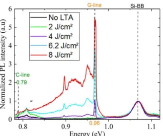
Fig. 1. PL spectra obtained on excimer laser-irradiated zone: C-line, G-line and Si-BB are identified by dotted lines respectively at 0.79, 0.96 and 1.07 eV. The star represent a bench artefact.
normalized with respect to the broad peak centered at 1.07 eV corresponding to the band-to-band transition of silicon. No other peaks are visible in this energy range in the non-annealed sample spectrum. In contrast, the annealed samples exhibit several peaks in a broad band extending from 0.78 to 1 eV. In addition, the intensity of this band increases with the energy density of the laserbeam. According to the literature, the peaks centered at 0.96 and 0.79 eV are attributed to the so called G-line and C-line, respectively, which clearly indicate that carbon- and oxygen-related defects are formed in the laser annealed samples [10]. Indeed, the G emission (due to the relaxation of excitonic transitions) is attributed to the presence of a Cs-Si-Ci complex with Cs and Ci corresponding to carbon atoms in substitutional and interstitial sites, respectively; similarly, the C-line emission is attributed to a Ci-Oi complex representing a carbon atom in interstitial site interacting with an oxygen atom also in interstitial position.
Fig. 2. TEM micrographs from Si samples annealed at different laser energy densities: 4 J/cm2 (a), and 6.2 J/cm2 (b).
0.88 0.90 0.92 0.94 0.96 0.1 0.2 0.3 0.4 0.5 0.6 0.7 PL i ntensit y (a.u) Energy (eV)
Fig. 3. PL spectra obtained from a sample annealed with an energy density of 8 J/cm2 where the G(TA) and E satellite lines bounds to the G-line peak
are identified.
In the energy range between 0.89 and 0.96 eV, light emission can be due to several defects: dislocations, which are responsible for the so called D-lines, or carbon-related defects which exhibit G-line satellite peaks in this same energy range [11]. The dislocation-related D-lines have been observed in plastically deformed silicon [12], epitaxial SiGe/Si stacks [13] or in multi-crystalline silicon (mc-Si) [14]. It was suggested that D-lines appear by pairs (D2/D1, D4/D3 and D5/D5’) because of their behavior in similar temperature intervals [15]. In particular, the D4 band is due to radiative transitions occurring within a shallow unidimensional band formed by the dislocations deformation field, while the D3 line is a phonon replica of D4 [15]. The D1 and D2 peaks are related to the presence of oxygen precipitates [16] and D5 and D5’ are caused by large dislocations [17].
We investigated several laser annealed samples by TEM and typical micrographs obtained from two of them are shown in Fig. 2. Both low magnification (cf. Fig. 2a) and high-resolution micrographs (cf. Fig. 2b) clearly indicate that the crystallinity of the Si structure is perfectly recovered after a melt laser anneal. The observed PL peaks in the 0.89-0.96 eV energy range cannot therefore be associated to dislocation related D-lines.
A zoom-in of the PL spectrum in this energy range for the sample annealed with 8 J/cm2 is shown in Fig. 3. A detailed analysis of this spectrum reveals that the observed peaks are satellite lines related to the G-line peak. In particular, in agreement with previous reports [11], the acoustic transverse phonon replica G(TA) is found at 0.949 eV while the E satellite peak corresponding to local mode related to the vibration of carbon is observed at 0.897 eV. The main properties of the observed peaks are summarized in Table I.
TABLE I. MAIN PROPERTIES OF THE G SATELLITE LINES.
Peaks Energy
(eV)
Gap with G-line (meV) Width (meV) G(TA) 0.949 19 10.2 E 0.897 71 1.05
G(TA)
E
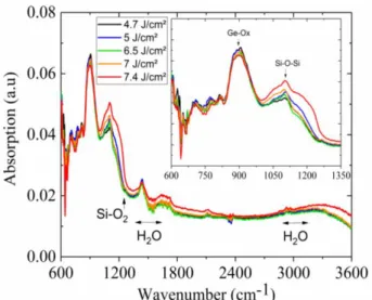
*Fig. 4. Absorption spectra obtained by FTIR on laser annealed samples. In addition to PL, the identification of defects was completed by FTIR (Fourier Transform InfraRed spectroscopy) measurements. In particular, FTIR was used to investigate the presence of oxygen in the laser annealed samples. To this purpose, the absorption by FTIR was measured using a germanium ATR (Attenuated Total Reflectance) accessory allowing to probe a thin silicon layer. Fig. 4 presents the absorption spectra of laser annealed samples with energy densities between 4.7 and 7.4 J/cm². The Ge-O2 peak located at ~900 cm-1 is due to the ATR accessory. The main difference between the measured spectra occurs at ~1100 cm-1, where a peak related to a Si-O-Si complex is observed (cf inset of Fig. 4) [18]. The intensity of the observed Si-O-Si signal increases when the laser energy increases confirming that the formation of this complex is enhanced by the laser annealing process. No other peaks are observed by FTIR in the annealed samples.
In summary, PL and FTIR analyses indicate that both C- and O-related defects are formed during melt laser annealing. In order to assess whether the C- and O- atoms contained in these defects originate from the substrate or are introduced into the structure during annealing, we investigated the C and O chemical concentration profiles in all the annealed samples.
B. Defects localisation
Oxygen and Carbon concentration profiles were measured by Secondary Ion Mass Spectrometry (SIMS) with a Cameca IMS-4FE6 system. In Fig. 5, oxygen depth profiles are reported for a reference non-annealed sample (black curve) and for samples annealed with energy densities in the range 2-8 J/cm2. Both the oxygen peak concentration and the penetration depth are found to increase with the laser energy density. In particular, the oxygen maximum penetration depth is in agreement with the calculated thickness of the melted regions (20 nm at 2 J/cm²; 450 nm at 4 J/cm²; 1000 nm at 6 J/cm²; 1600 nm at 8 J/cm²), which is compatible with an oxygen source being located at the sample surface, while the released oxygen fastly diffuses in the liquid phase down to the liquid/solid interface. It is therefore suggested that the thin native oxide located at the surface during anneal (whose thickness is typically between 1 and 2 nm) is the source of the observed oxygen impurities. Indeed, even the maximum dose of oxygen measured by
Fig. 5. SIMS profiles of oxygen concentration in depth generated by annealed laser for various laser energy
SIMS in the sample annealed at 8 J/cm2 (5.1014 at/cm²) is lower (~75 %) than the amount of oxygen atoms contained in a 1 nm-thick oxide layer.
Finally, for the highest laser energy density investigated in this work (8 J/cm2), an immobile peak is observed at ~200 nm below the surface, at concentrations above ~5x1018 cm-3. This concentration value corresponds to the known solubility limit of oxygen in liquid silicon [19], suggesting that oxygen precipitation occur in the liquid phase during anneal and is “quenched” in the solid phase after recrystallisation.
SIMS analysis was also used to investigate the presence of carbon in the laser annealed samples. The measured C profile from the sample annealed at 8 J/cm2 is reported in Fig. 6 together with the corresponding oxygen profile. For comparison, the C and O profiles from the non-annealed reference sample are also reported in the figure. Similarly to oxygen, C is found to penetrate from the surface during anneal and diffuse (without precipitation) down to the liquid/solid interface. This suggest that Carbon contaminants, generally contained in the surface native oxide, are the source of the observed profile. Indeed, SIMS analysis from a samples containing a surface “clean” thermal oxide showed no carbon penetration during laser anneal (not shown).
Fig. 6. Comparison of SIMS profiles of oxygen concentration and carbon of no-annealed sample and annealed sample by laser at 8 J/cm² with 10 pulses.
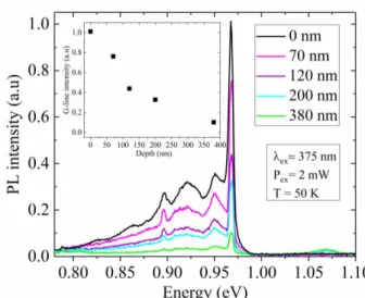
Fig. 7. PL spectra obtained on sample annealed at 8 J/cm² at different depth.
These results therefore suggest that the optical defects observed in laser annealed samples (C- and G- lines in PL spectra, cf. Fig. 1) originate from the oxygen and carbon impurities contained in the surface native oxide that diffuse into the substrate during anneal. In order to confirm this scenario, we etched the 8 J/cm² annealed sample at different depths and observed the corresponding luminescence spectra. The spectra acquired on the sample without etching and etched at 70, 120, 200 and 380 nm depth (as measured by mechanical profilometer) are reported in Fig. 7. The spectra were acquired with a 375 nm laser, whose penetration depth in silicon is ~20 nm. To compare the spectra, the acquisition parameters and the experimental conditions are strictly identical. All investigated samples exhibit similar PL spectra, including C-lines, lines and G-satellite lines. However, the peak intensity is found to decrease when increasing the etch depth. An example is given in the inset for the G-line intensity. Considering the small penetration depth of the incoming laser (~20 nm), these results clearly indicate that the decrease of the PL intensity with depth is in perfect agreement with the decrease of C and O concentrations, measured by SIMS, confirming that they are the cause of the observed PL signal. This is also supported by the corresponding increase in the intensity of the Si-BB peak (at ~1.06 eV) when increasing the etch depth. Indeed, when increasing the etch depth, the contribution of the undamaged Si substrate to the overall PL spectrum becomes more prominent.
IV. CONCLUSION
In this work, we presented a comprehensive investigation of laser induced damage in silicon by implementing a methodology allowing the identification and the localization of the defects.
PL analyses combined with TEM reveals that laser annealed samples reveal the presence of Carbon and Oxygen related defects, in the form of C-line and G-lines (including the associated G satellite lines). Additional Oxygen related defects (Si-O-Si complexes) were revealed by FTIR analysis. Based on SIMS analyses combined with chemical etch, it is found that the optical defects observed in laser annealed samples originate from the oxygen atoms and carbon impurities contained in the surface native oxide from which
they are released and subsequently diffuse into the substrate during anneal down to the liquid/solid interface.
ACKNOWLEDGMENT
This work was financially supported by the Nano2017 French programme. This work was partly supported by LAAS-CNRS micro and nanotechnologies platform member of the French RENATECH network.
REFERENCES
[1] T. Sarnet, M. Hernandez, and D. Débarre, “Dopage laser en microélectronique,” Journal de Physique IV (Proceedings), vol. 138, no. 1, pp. 203–212, Dec. 2006.
[2] K. Huet, F. Mazzamuto, T. Tabata, I. Toqué-Tresonne, and Y. Mori, “Doping of semiconductor devices by Laser Thermal Annealing,” Materials Science in Semiconductor Processing, vol. 62, pp. 92–102, May 2017.
[3] P. Gundel, D. Suwito, U. Jager, F. D. Heinz, W. Warta, and M. C. Schubert, “Comprehensive Microscopic Analysis of Laser-Induced High Doping Regions in Silicon,” IEEE Transactions on Electron Devices, vol. 58, no. 9, pp. 2874–2877, Sep. 2011.
[4] V. Privitera et al., “Integration of Melting Excimer Laser Annealing in Power MOS Technology,” IEEE Transactions on Electron Devices, vol. 54, no. 4, pp. 852–860, Apr. 2007.
[5] M. Ametowobla, G. Bilger, J. R. Köhler, and J. H. Werner, “Laser induced lifetime degradation in p-type crystalline silicon,” Journal of Applied Physics, vol. 111, no. 11, p. 114515, Jun. 2012.
[6] Y.-J. Han, E. Franklin, A. Fell, M. Ernst, H. T. Nguyen, and D. Macdonald, “Low-temperature micro-photoluminescence spectroscopy on laser-doped silicon with different surface conditions,” Applied Physics A, vol. 122, no. 4, pp. 1-10, Apr. 2016.
[7] H. T. Nguyen, Y. Han, M. Ernst, A. Fell, E. Franklin, and D. Macdonald, “Dislocations in laser-doped silicon detected by micro-photoluminescence spectroscopy,” Applied Physics Letters, vol. 107, no. 2, p. 022101, Jul. 2015.
[8] N. A. Drozdov, A. A. Patrin, and V. T. Tkachev, “Modification of the Dislocation Luminescence Spectrum by Oxygen Atmospheres in Silicon”, phys. stat. sol (a) 64, pp. 63-65, 1981.
[9] J. Mooney and P. Kambhampati, “Get the Basics Right: Jacobian Conversion of Wavelength and Energy Scales for Quantitative Analysis of Emission Spectra,” The Journal of Physical Chemistry Letters, vol. 4, no. 19, pp. 3316–3318, Oct. 2013.
[10] M. Tajima, H. Kiuchi, F. Higuchi, and A. Ogura, “Quantification of C in Si by photoluminescence at liquid N temperature after electron irradiation,” Applied Physics Express, vol. 10, no. 4, p. 046602, Apr. 2017.
[11] A. Lazrak, “Etude par photoluminescence des centres associés à l’oxygène et au carbone dans le silicium,” Thesis, Université de Grenoble, 1984.
[12] N. A. Drozdov, A. A. Patrin and V. D. Tkachev, “Recombination radiation on dislocations in silicon”, Journal of Experimental and Theoretical Physics Letters, Vol. 23, p.597, 1976.
[13] V. V. Kveder, E. A. Steinman and H. G. Grimmeiss, “Photoluminescence studies of relaxation processes in strained Si1-x Ge x /Si epilayers”, J. Appl. Phys. Vol. 78, pp 446-450, 1995.
[14] I. Tarasov, S. Ostapenko, C. Hassler and E. U. Reisner, “Spatially resolved defect diagnostics in multicrystalline silicon for solar cells”, Mater. Sci. Eng. Vol. B 71, pp. 51-55, 2000.
[15] S. Ostapenko, I. Tarasov, J. P. Kalejs, . Hassler and E. U. Reisner, “Defect monitoring using scanning photoluminescence spectroscopy in multicrystalline silicon wafers”, Semicond. Sci. Technol., Vol. 15, pp. 840-848, 2002.
[16] S. Pizzini, M. Guzzi, E. Grilli and G. Borionetti, “The photoluminescence emission in the 0.7-0.9 eV range from oxygen precipitates, thermal donors and dislocations in silicon”, J. Phys.: Condens. Matter, Vol. 12 pp. 10131-10143, 2000.
[17] R. Sauer, J. Weber, J. Stolz, E. R. Weber, K.-H. Küsters, and H. Alexander, “Dislocation-related photoluminescence in silicon,” Applied Physics A, vol. 36, no. 1, pp. 1–13, 1985.
[18] V. P. Tolstoy, I. V. Chernyshova and V. A. Skryshevsky, "Handbook of Infrared Spectroscopy of Ultrathin Films", Wiley/Interscience, Hoboken, 2003.
[19] Y. Yatsurugi, et. al., “Concentration, Solubility, and Equilibrium Distribution Coefficient of Nitrogen and Oxygen in Semiconductor Silicon”. J. Electrochem. Soc., Vol. 120, pp. 975-979, 1973.