HAL Id: hal-01955720
https://hal.laas.fr/hal-01955720
Submitted on 14 Dec 2018
HAL is a multi-disciplinary open access
archive for the deposit and dissemination of
sci-entific research documents, whether they are
pub-lished or not. The documents may come from
teaching and research institutions in France or
abroad, or from public or private research centers.
L’archive ouverte pluridisciplinaire HAL, est
destinée au dépôt et à la diffusion de documents
scientifiques de niveau recherche, publiés ou non,
émanant des établissements d’enseignement et de
recherche français ou étrangers, des laboratoires
publics ou privés.
Normally-Off AlGaN/GaN HEMT using fluorine
implantation below the channel
Saleem Hamady, Frédéric Morancho, Bilal Beydoun, Patrick Austin, Mathieu
Gavelle
To cite this version:
Saleem Hamady, Frédéric Morancho, Bilal Beydoun, Patrick Austin, Mathieu Gavelle. Normally-Off
AlGaN/GaN HEMT using fluorine implantation below the channel. Symposium en Génie Electrique
2014 (SGE 2014), Jul 2014, Cachan, France. �hal-01955720�
SYMPOSIUM DE GÉNIE ELECTRIQUE (SGE’14) : EF-EPF-MGE 2014, 8-10 JUILLET 2014, ENS CACHAN, FRANCE
Normally-Off AlGaN/GaN HEMT using fluorine
implantation below the channel
Saleem HAMADY
1,2,4, Frédéric MORANCHO
1,3, Bilal BEYDOUN
4, Patrick AUSTIN
1,3, Mathieu GAVELLE
51CNRS, LAAS, 7 avenue du colonel Roche, F-31400 Toulouse, France 2Univ de Toulouse, LAAS, F-31400 Toulouse, France
3Univ de Toulouse, UPS, LAAS, F-31400 Toulouse, France 4GET/LPE, Lebanese University, Hadath campus, Beirut, Lebanon
5CEA Tech Midi-Pyrénées, 2 avenue Édouard Belin F31055 Toulouse Cedex 4, France
E-Mail: [email protected], [email protected], [email protected], [email protected], [email protected]
RESUME - AlGaN/GaN HEMTs are very promising candidates for high frequency applications with high power and low noise. Unfortunately, while switching applications strongly demand normally-off operation, conventional HEMTs are normally-on. For the sake of achieving normally-off HEMTs, several structures have been proposed. One of the major normally-off HEMTs uses fluorine implantation in the AlGaN layer. We suggest in this work the implantation of fluorine ions under the AlGaN/GaN interface only below the gate electrode rather than implanting in the AlGaN layer. Simulation results show that the proposed method is capable of achieving normally-off operation and more effective when it comes to the fluorine concentration required to obtain the desired threshold voltage. Neither the vertical breakdown voltage, nor the off-state current are affected by this approach.
Keywords— TCAD simulation, normally-off, Gallium Nitride (GaN), High electron mobility transistor (HEMT), fluorine implantation
1. INTRODUCTION
The High Electron Mobility Transistor (HEMT) is a field effect transistor in which two layers of different bandgaps and polarization fields are grown upon one another. As a consequence of the discontinuity in the polarization field, surface charges at the heterointerface are created. If the induced charge is positive, electrons will tend to compensate the induced charge resulting in the formation of a two dimensional electron gas (2DEG) [1]. Thanks to the GaN properties and the HEMT’s topology, AlGaN/GaN HEMTs are now promising devices for high frequency applications with high power and low noise, such as microwave and millimeter wave communications, imaging and radars [2].
In the conventional HEMT, the energy levels of the triangular quantum well, formed in the GaN layer below the AlGaN/GaN interface, are below the Fermi level at equilibrium. This will make the channel populated with electrons at zero gate voltage, hence making the HEMT normally-on. However, for power switching applications, normally-off operation is strongly required [3]. In order to achieve normally-off operation, the energy levels must be lifted above the Fermi level. Several structures have been proposed
for the realization of normally-off AlGaN/GaN HEMT such as recessed gate structures [4], fluorine ion treatment [5], pn junction gate structures [6], thin AlGaN barrier[7], AlN/GaN structure [8] and conventional HEMT with InGaN cap layer [9]. In the normally-off HEMT reported in [5], fluorine ions are implanted in the barrier layer (AlGaN layer). When this approach is used, small amount of fluorine ions penetrate into the channel formed at the AlGaN/GaN interface, presenting themselves as impurities that lead to mobility degradation [10]. In this paper, we propose to implement the ions below the channel (in the GaN layer) under the AlGaN/GaN interface, and that only below the gate electrode. To obtain this structure, the following can be done: after growing the buffer and GaN layers, fluorine ions will be implanted. Then the channel layer of GaN (15 nm) will be introduced, and above all comes the AlGaN layer (barrier layer). This way, no scattering will occur between the 2DEG and the fluorine ions since the fluorine ions are below the channel region.
2. SIMULATION STRATEGY
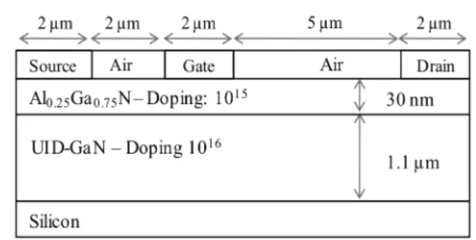
ATLAS, a physically-based TCAD simulation tool from Silvaco, is used to analyze the new HEMT structure. Physical models of the simulator are based on Shockley-Read Hall recombination, Fermi-Dirac statistics and field-dependent mobility [11]. The simulator is calibrated by using real parameters of a normally-on HEMT device, as shown in figure 1.
Fig. 1. Schematic cross-section of the normally-on HEMT structure used for the calibration of the TCAD simulations.
Add “cm-3” after 1015 and 1016 in the figure 1.
In figure 2, the simulation results are presented and compared with the experimental transfer characteristics Id (Vgs). A good match is observed for the threshold voltage
(Vth) and the transconductance (gm). During calibration, the
energy and the concentration of the acceptor traps as well as the density of the 2DEG were tuned. In Table 1, some of the parameters used for the simulation are illustrated.
Fig. 2. Comparison of experimental and simulated Id(Vgs) transfer characteristics showing a clear match for the threshold voltage and transconductance.
Table 1: HEMT simulation parameters
To simulate the effect of the implanted fluorine ions, negative charge was added inside the GaN (or AlGaN) layer. To do that using ATLAS, the GaN (or AlGaN) layer was split into two layers. This will generate an interface (GaN/GaN or AlGaN/AlGaN homo-interface) inside the layer. At this interface, a fixed negative charge is added. Although the profile of the fluorine ions concentration, resulting from this approach, differs from the profile experimentally obtained, its effect on the transfer characteristics can be imitated by varying the concentration of negative charge at the interface.
3. SIMULATION RESULTS
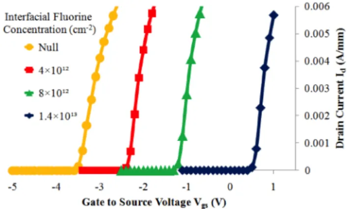
3.1. Fluorine implantation in AlGaN layer
Figure 3 shows the transfer characteristics of the conventional normally-on HEMT of figure 1 (“Null”) and HEMTs with fluorine implanted in AlGaN (figure 4) at various concentrations (from 4 × 10¹² to 1.4 × 1013 cm-2). The distance
between the fluorine ions and the AlGaN/GaN interface is taken 15 nm. It is clear that, at a certain fluorine concentration (1.4 × 1013 cm-2), this technique is capable of shifting the
threshold voltage to a positive value (0.5 V), making the HEMT normally-off.
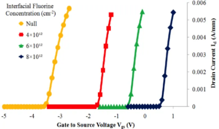
3.2. Fluorine implantation in the GaN layer
Figure 5 shows the transfer characteristics of the conventional normally-on HEMT of figure 1 (“Null”) and HEMTs with
Fig. 3. Id (Vgs) transfer characteristics of the conventional normally-on HEMT and HEMTs with fluorine implanted in AGaN at various concentration.
Fig. 4. Schematic cross-section of the simulated HEMT with fluorine implanted in the AlGaN layer.
Density of acceptor traps 1017 cm-3 Energy of acceptor traps 0.41 eV
Interfacial charge density k( PGaN - PAlGaN) / q cm-2
fluorine implanted in the GaN layer (Figure 6) at different concentrations (from 4 × 10¹² to 8 × 1012 cm-2). The distance
between the fluorine ions and the AlGaN/GaN interface is also taken to be 15 nm. As the fluorine concentration increases, the threshold voltage increases to positive values, confirming that our technique is also capable of achieving normally-off HEMT.
It can be seen from figures 3 and 5 that although the same threshold voltage (0.5 V) was achieved after implantation in both cases, the fluorine concentration required to achieve the desired threshold voltage is lower (8×10¹² < 14×1012) when implantation is performed in the GaN layer rather than in the AlGaN layer, making our proposed technique more efficient. 4. ENERGY BAND DIAGRAM
To further explore the consequences of the two different techniques, the band diagrams for the two structures are shown in figure 7. It can be concluded from this figure that the implantation in GaN is more effective: since HEMTs attain Schottky gates, the conduction band at the top of the AlGaN layer is pinned at a fixed energy equals to the Schottky barrier. If it was not for that pinning, the conduction band in AlGaN would have risen higher when fluorine is implanted, causing a higher shift in the threshold voltage. Moreover, it can be noted, from the band diagram, that the confinement of the 2DEG under the gate is superior in the case of Fluorine implanted in GaN (see zoom in Figure 7).
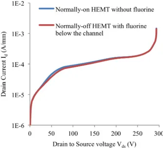
5. BREAKDOWN AND OFF-STATE CURRENT
To examine the off-state current and the breakdown voltage, the structure shown in figure 6 was studied. However,
Fig. 5. Id (Vgs) transfer characteristics of the conventional normally-on HEMT and HEMT with fluorine implanted in GaN at various concentration.
Fig. 6. Schematic cross-section of the simulated HEMT with fluorine implanted in the GaN layer
Fig. 7: Band diagrams of HEMT with fluorine implanted in AlGaN at concentration 1.4×1013cm-2 and HEMT with fluorine in GaN at concentration 8×1012cm-2; both HEMTs attain a threshold voltage of 0.5 V.
an x-mole fraction of 0.15 was used instead (YOU HAVE TO EXPLAIN HERE, IN ONE SENTENCE, WHY YOU HAVE CHANGED THE X-MOLE FRACTION). In this case, a fluorine concentration of 4.2 × 1012 cm-2 is necessary to achieve
normally-off operation with a threshold voltage of 0.5 V. The same HEMT with no fluorine implantation attains a threshold voltage of -2 V.
Figure 8 shows the variation of the drain current with the applied drain to source voltage Id(Vds). The applied gate to
source voltage is: Vgs = Vth - 1 V, in order to study the two
HEMTs in the off-state, i.e. below their threshold voltage. It is clear that neither the vertical breakdown voltage, nor the off-state current are affected by the implanted fluorine ions. A breakdown voltage of 280 V was obtained in both cases.
6. CONCLUSION
In this work, for the sake of obtaining a normally-off HEMT, we suggest the implantation of fluorine ions in the GaN layer, under the AlGaN/GaN interface only below the gate electrode, rather than the implantation in the AlGaN layer as previously proposed in other papers. Using numerical simulations, we have shown that this approach is capable of shifting the threshold voltage to positive values. In addition to that, this technique is more effective when it comes to the
concentration required to achieve normally-off operation. Moreover, with this technique, the channel electrons will be better confined below the gate and scattering with fluorine ions will vanish, since fluorine is implanted below the channel layer. Finally, the implantation of fluorine ions below the channel does not affect the vertical breakdown voltage and the off-state current.
7. ACKNOWLEDGMENT
This work was funded by the Laboratory for Analysis and Architecture of Systems (LAAS – CNRS/France) and by GET/EDST/UL- AZM & SAADA association.
8. REFERENCES
[1] H. Chen, J. Wang, C. Xu, M. Yu, Y. Fu, Z. Dong, F. Xu, Y. Hao, and C. P. Wen, “Enhanced device performance of AlGaN/GaN HEMTs using thermal oxidation of electron-beam deposited aluminum for gate oxide,” in 9th International Conference on Solid-State and
Integrated-Circuit Technology, 2008. ICSICT 2008, 2008, pp. 1443–1446.
[2] U. K. Mishra, P. Parikh, and Y.-F. Wu, “AlGaN/GaN HEMTs-an overview of device operation and applications,” Proc. IEEE, vol. 90, no. 6, pp. 1022–1031, 2002.
[3] H. Kambayashi, Y. Satoh, T. Kokawa, N. Ikeda, T. Nomura, and S. Kato, “High field-effect mobility normally-off AlGaN/GaN hybrid MOS-HFET on Si substrate by selective area growth technique,”
Solid-State Electron., vol. 56, no. 1, pp. 163–167, Feb. 2011.
[4] S. D. Burnham, K. Boutros, P. Hashimoto, C. Butler, D. W. S. Wong, M. Hu, and M. Micovic, “Gate-recessed normally-off GaN-on- Si HEMT using a new O2-BCl3 digital etching technique,” Phys. Status
Solidi C, vol. 7, no. 7–8, pp. 2010–2012, 2010.
[5] H. Chen, M. Wang, and K. J. Chen, “Self-aligned enhancement-mode AlGaN/GaN HEMTs using 25 keV fluorine ion implantation,” in
Device Research Conference (DRC), 2010, 2010, pp. 137–138.
[6] X. Hu, G. Simin, J. Yang, M. A. Khan, R. Gaska, and M. S. Shur, “Enhancement mode AlGaN/GaN HFET with selectively grown pn junction gate,” Electron. Lett., vol. 36, no. 8, pp. 753–754, 2000. [7] Y. Ohmaki, M. Tanimoto, S. Akamatsu, and T. Mukai,
“Enhancement-Mode AlGaN/AlN/GaN High Electron Mobility Transistor with Low On-State Resistance and High Breakdown Voltage,” Jpn. J. Appl.
Phys., vol. 45, no. No. 44, pp. L1168–L1170, Nov. 2006.
[8] M. Higashiwaki, T. Mimura, and T. Matsui, “Enhancement-Mode AlN/GaN HFETs Using Cat-CVD SiN,” IEEE Trans. Electron
Devices, vol. 54, no. 6, pp. 1566–1570, 2007.
[9] T. Mizutani, M. Ito, S. Kishimoto, and F. Nakamura, “AlGaN/GaN HEMTs With Thin InGaN Cap Layer for Normally Off Operation,”
IEEE Electron Device Lett., vol. 28, no. 7, pp. 549–551, 2007.
[10] K. J. Chen, L. Yuan, M. J. Wang, H. Chen, S. Huang, Q. Zhou, C. Zhou, B. K. Li, and J. N. Wang, “Physics of fluorine plasma ion implantation for GaN normally-off HEMT technology,” in Electron
Devices Meeting (IEDM), 2011 IEEE International, 2011, pp. 19.4.1–
19.4.4.
[11] SILVACO, “ATLAS User’s Manual DEVICE SIMULATION SOFTWARE,” Santa Clara, CA,, 2011, pp. 330–331.
Fig. 8. Simulated Id(Vds) characteristics in the state, showing the off-state current and the breakdown voltage of the normally-on HEMT and the normally-off HEMT with fluorine implantation below the channel.