HAL Id: tel-01627309
https://tel.archives-ouvertes.fr/tel-01627309
Submitted on 1 Nov 2017
HAL is a multi-disciplinary open access archive for the deposit and dissemination of sci-entific research documents, whether they are pub-lished or not. The documents may come from teaching and research institutions in France or abroad, or from public or private research centers.
L’archive ouverte pluridisciplinaire HAL, est destinée au dépôt et à la diffusion de documents scientifiques de niveau recherche, publiés ou non, émanant des établissements d’enseignement et de recherche français ou étrangers, des laboratoires publics ou privés.
optics
Emanuel Thomas Peinke
To cite this version:
Emanuel Thomas Peinke. All-optical ultrafast switching of semiconductor micropillar cavities : basics and applications to quantum optics. Materials Science [cond-mat.mtrl-sci]. Université Grenoble Alpes, 2016. English. �NNT : 2016GREAY030�. �tel-01627309�
Pour obtenir le grade de
DOCTEUR DE L’UNIVERSITÉ DE GRENOBLE
Spécialité : Physique / Nanophysique
Arrêté ministérial : 7 août 2006
Présentée par
Emanuel Thomas P
EINKE
Thèse dirigée par Jean-Michel GÉRARD
et encadrée par Joël BLEUSE
préparée au sein de l’équipe mixte CEA-CNRS « Nanophysique et Semiconducteurs », CEA / INAC-PHELIQS , F-38054 Grenoble
à l’École Doctorale de Physique de Grenoble
Commutation tout optique ultra-rapide de
micropiliers semi-conducteurs : propriétés
fondamentales et applications dans le
domaine de l’optique quantique
All-optical ultrafast switching of semiconductor
micropillar cavities: basics and applications to
quan-tum optics
Thèse soutenue publiquement le 5 avril 2016, devant le jury composé de :
M. Benoît BOULANGER Président du jury M. Alfredo DE ROSSI Rapporteur M. Philippe ROUSSIGNOL Rapporteur M. Willem L. VOS Examinateur M. Jean-Michel GÉRARD Directeur de thèse M. Joël BLEUSE Encadrant de thèse
Pour commencer ce manuscrit, je tiens à remercier toutes les personnes qui m’ont soutenues et inspirées pendant ces trois années de thèse. Grâce à eux, ce fut une expérience en-richissante et inoubliable. J’espère que le résultat, ce manuscrit, saura refléter ceci et convaincre le lecteur.
Mes encadrants m’ont été indispensables. Jean-Michel Gérard, mon directeur de thèse, pour son accompagnement et son engagement tout le long de cette thèse. Ses idées novatri-ces et son enthousiasme sont certainement deux piliers de cette thèse, et m’ont permis de l’accomplir avec grande satisfaction. Joël Bleuse, mon encadrant, m’a appris à maîtriser les différentes expériences optiques et m’a fortement soutenue pendant la rédaction. A l’écoute de toutes mes questions, soit-elles sur la recherche ou sur le plan personnel, je pouvais toujours me confier à lui — sans oublier nos nombreuses discussions sur la so-ciété et la politique. Enfin, Julien Claudon, à qui j’ai pu adresser toutes mes questions sur la physique et discuter des difficultés de programmation rencontrées (ou encore parler d’exploits en montagne).
Je tiens également à remercier les membres du jury qui ont accepté de m’évaluer et m’ont donné un retour précieux sur ce manuscrit : Benoît Boulanger, président du jury, Philippe Roussignol et Alfredo De Rossi, rapporteurs, et Willem L. Vos, examinateur. Merci à vous pour vos remarques et ce moment fort agréable que nous avons passé lors de ma soutenance. Un grand merci aux techniciens Yann Genuist, Didier Boilot et Yoann Curé. Yann, Didier et moi avons repris ensemble la main sur le bâti d’épitaxie III-As — après que Emmanuel Dupuy m’ait introduit dans ce domaine — et ce fut un grand plaisir de travailler en trinôme : Yann l’expert de la croissance moléculaire, Didier l’expert de la science du vide, et moi le physicien. Nous avons toujours eu le soutien de Yoann. Outre la croissance, j’ai beaucoup apprécié sa complicité et son aide dans la programmation et le développement de codes. Sur ce point je remercie également Jan-Peter Richters, qui au début de ma thèse était mon expert Linux et programmation, et Yohan Désières, qui m’a initié aux simulations FDTD.
cale. Un des moments forts de cohésion et d’amitié était la pause-café matinale. Puis les secrétaires côté CEA, Carmelo Castagna et Céline Conche, qui m’ont fortement facilité toutes les démarches administratives grâce à leur compétence et leur efficacité. Et bien sur tous les stagiaires, thésards et post-docs, Thomas, Rob, Tobi, Tomek, Quentin, Petr, Mark, Damien+Damien, Manos, Adrien, Pamela, . . . qui sont devenus des amis.
Merci aussi à mes collaborateurs, Gaston Hornecker et Alexia Auffèves (de notre groupe), avec lesquels j’ai travaillé sur le « pulse shaping » et à Willem L. Vos et Henri Thyrrestrup des COPS de l’université de Twente avec lesquels nous avons eu un riche échange autour des expériences de « cavity switching ».
Bien sûr, merci à mon successeur Tobias Sattler pour tout le travail, le rire et les aventures ensemble. Je suis aussi reconnaissant à Adrien Delga qui m’a lithographié des échantillons et à Petr Stepanov avec lequel j’ai eu le plaisir de partager des expériences d’optique.
Finalement tous mes amis de Grenoble et de la région, ma famille, et ma copine Sara. Merci à vous tous,
Introduction 5
1 Physical concepts of optical microcavities 9
1.1 Confinement of the electromagnetic field . . . 9
1.1.1 Spatial confinement . . . 9
1.1.2 Spatial confinement: the mode volume . . . 11
1.1.3 Temporal storage and the quality factor Q . . . 12
1.2 Semiconductor microcavities . . . 14
1.2.1 Properties of distributed Bragg reflectors . . . 16
1.2.2 Planar cavities . . . 19
1.2.3 Micropillars . . . 20
1.3 Applications of semiconductor microcavities . . . 23
1.3.1 Spectral filtering . . . 23
1.3.2 Cavity Quantum Electrodynamic (CQED) . . . 24
1.3.3 Low threshold microlasers . . . 30
1.3.4 Bright single-mode single photon sources . . . 31
1.4 Cavity switching . . . 32
1.4.1 Changing the refractive index of semiconductors . . . 32
1.4.2 Applications of cavity switching . . . 33
1.5 Conclusion . . . 34
2 Sample production and characterization 35 2.1 Conception of a planar microcavity . . . 35
2.2 Molecular beam epitaxy . . . 36
2.2.1 The principle of MBE growth . . . 36
2.2.2 Sample preparation and growth conditions . . . 38
2.2.3 The RHEED . . . 39
2.2.4 Growth of planar cavities . . . 40
2.2.5 Growth of InAs quantum dots . . . 41
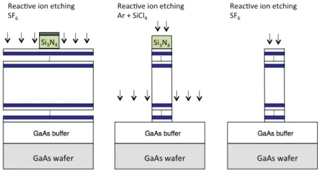
2.3 Top-down fabrication of a pillar microcavity . . . 44
2.4 Optical characterisation . . . 46
2.4.1 The FTIR . . . 46
2.4.2 Micro-photoluminescence . . . 47
2.4.3 Time resolved spectral analysis with a streak camera . . . 48
2.5 Numerical methods . . . 50
2.5.1 The transfer matrix method . . . 50
2.5.2 FDTD . . . 54
2.6 Conclusion . . . 55
3 Cavity Switching experiments by all-optical free carrier injection. 57 3.1 Switching microcavities . . . 57
3.2 Our experimental approach: Probing cavity switching with an internal light source . . . 58
3.3 Characterising switching events in micropillar cavities . . . 62
3.3.1 “Switch-on” behaviour . . . 63
3.3.2 Free carrier relaxation and the spectral return of the cavity mode . . 64
3.3.3 Switching amplitude . . . 73
3.4 Differential switching of micropillar cavity modes . . . 79
3.4.1 Differential switching of a small micropillar . . . 80
3.4.2 Simulation of differential switching . . . 81
3.4.3 Differential switching of an ellipsoid micropillar . . . 84
3.4.4 Differential switching of a big micropillar . . . 86
3.5 Conclusion . . . 90
4 Theory of Purcell switching and related applications 91 4.1 About the real-time control of an emitter in a microcavity . . . 91
4.2 Mathematical description of the time- and energy-dependent coupling of a QD in a cavity . . . 93
4.2.1 Rate equations . . . 94
4.2.2 Quantum Langevin equations for a QD in a cavity . . . 95
4.3 Purcell switching . . . 96
4.4 Temporal shaping of single photon pulses . . . 101
4.4.1 Photon emission fidelity and efficiency . . . 102
4.4.2 Shaping of time-domain Gaussian and exponentially increasing single photon pulses, using cavity switching . . . 103
4.4.3 Efficient emission and consecutive reabsorption of single photon pulses112 4.4.4 Using emitter tuning to shape single photon pulses . . . 120
4.5 Conclusion . . . 124
5 Experimental applications of cavity switching 125 5.1 Generation of ultrashort spontaneous emission bursts using cavity switching 125 5.1.1 Single burst generation . . . 126
5.1.2 Double burst . . . 130
5.1.3 Dependence of tburst with the amplitude of the switch . . . 132
5.2 Is there Purcell switching in the experiments? . . . 138
5.3 Switching a planar high-Q cavity with the application to change the colour of the trapped light . . . 140
5.3.1 The high-Q planar cavity . . . 140
5.3.2 The cavity ring-down measurement . . . 142
5.3.3 Changing the colour of the light trapped in a planar cavity . . . 143
5.4 Conclusion . . . 150
Conclusion and perspectives 153
Semiconductor optical microcavities have been intensively studied since the late 80’s, due to their strong interest for basic experiments on light-matter interaction as well as for applications. To give only a few examples, microcavity lasers are nowadays widely used in telecoms and datacoms, while ring microcavities are key components used for filtering and reconfigurable routing in photonic chips.
On a more fundamental side, semiconductor microcavities containing quantum dots (QDs) have been used to reproduce in a solid-state system the famous Cavity Quantum ElectroDynamics (CQED) experiments initially performed on real atoms by the 2012 No-bel Prize laureate Serge Haroche [1]. In these experiments, semiconductor QDs are used as artificial atoms. Major basic effects such as the enhancement or inhibition of the QD spon-taneous emission [2, 3, 4], or the strong coupling regime between a single QD and a cavity mode [5, 6], have been demonstrated. Microcavities provide in fact a nearly perfect con-trol of QD spontaneous emission, which opens the way to important novel applications in optoelectronics and quantum information science. Noticeably, highly efficient single-mode single-photon sources have been realized by exploiting the Purcell effect (spontaneous emis-sion enhancement) for a single QD in a GaAs/AlAs microcavity [7, 8, 9].
While tuning techniques have been developed to control the frequency of the cavity modes [10], or the detuning and thus the interaction of cavity modes and embedded emit-ters, such techniques are usually very slow compared to the relevant time scales of the system (such as the storage time of the light in the cavity, or the emission lifetime of an embedded QD). Cavity switching, i.e. the ability to tune the frequency of the modes of a cavity in an ultrafast way [11, 12, 13, 14], opens far-reaching perspectives, such as the control in real time of the properties of an emitter in a cavity. Another application consists in changing the colour of light trapped in a cavity, and demonstrated experimentally by the group of M. Lipson using ring resonators [11] and later by Tanabe et al. using a photonic crystal cavity [15].
The objective of this thesis was to study in a time-resolved way — using a streak-camera with picosecond resolution — all-optical switching of microcavities having integrated solid state emitters. This work is in the continuity of my “Diplomarbeit” [16] and therefore contains some similarities with it. The cavity switching — i.e. the energy shift of the cavity mode — was realised in the picoseconds or few tens of picoseconds time-range. The time-dependent interactions of emitter and cavity mode were studied and the final goal was to control in real time the spontaneous emission dynamics of an emitter integrated in a micropillar cavity.
My contribution can be separated in three main parts: growth, simulation and optical analysis.
• With the molecular beam epitaxy (MBE) I grew mainly GaAs, AlAs, AlGaAs bi-dimensional layers and also InAs QDs. On this basis planar microcavities, solid-state emitters, and other structures were grown. In this manuscript I will only focus on the QD and microcavity production.
• I wrote Matlab, Octave and Python scripts to simulate on the transfer-matrix method (TMM), on the Finite-Difference in the Time Domain (FDTD) method, on diffusion, recombination and guided modes in micropillars and on solving differential equations like rate equations and quantum Langevin equations. This ensemble of developed numerical methods allowed me to design cavity samples with the desired properties, to analyse as-grown samples and to predict and study the feasibility of the differ-ent cavity switching experimdiffer-ents. Furthermore theoretical studies about the time-dependent coupling of an emitter and a cavity mode could be carried out, leading to results about the temporal shaping of single photon pulses.
• The optical characterisations were mostly about studying microcavities and the pho-toluminescence of emitters. With Fourier Transform Infra-Red (FTIR) spectroscopy I obtained information about reflectivity and modal structure of as-grown cavities. With macroscopic photoluminescence (excitation and collection of milimetre big structures) I studied ensembles of as-grown InAs-QDs. The micro-photoluminescence enabled me to study emitters integrated in structures on the micrometre scale — e.g. micropillar cavities.
The main part of the optical analysis were about cavity switching. They were done by time-resolved micro-photoluminescence measurements. For this purpose we ob-tained a new streak-camera with a picosecond temporal resolution. I mounted a new setup on the optical table, which was adapted to the switching of micrometre size cavities and could be operated in reflection (e.g. to study micropillar cavities) or in transmission (e.g. to study planar cavities). A frequency tunable pulsed- and a con-tinuous wave-laser could simultaneously be used as pump or probe. When operating under reflection, the samples could be placed in a cold-finger cryostat and at low temperature (about 7 K), in order to optimise the emission properties of the QDs. This thesis is organized as follows:
Chapter 1 Optical solid-state microcavities are introduced and their physical concepts discussed. Different types of cavities and their light storage and confinement properties — with the corresponding figures of merit, the quality factor Q and the effective mode volume Vef f — will be discussed. Introducing emitters inside the cavities we can speak
about spontaneous emission and cavity quantum electrodynamics (CQED). We will see different applications. Finally cavity switching — a dynamic modification of the cavity mode resonance — is introduced. It is the fundamental concept for this work.
Chapter 2 The production of microcavities and the integration of solid-state emitters, notably quantum dots, will be explained. The molecular beam epitaxy (MBE) plays a central role. We will see how to analyse the produced samples optically and introduce the numerical simulations used to concept the samples and predict the cavity switching experiments.
Chapter 3 We present a detailed experimental study of the switching of micropillar modes using all-optical free carrier injection. The spontaneous emission of a QD ensemble is used as internal light source, so as to probe by time-resolved photo-luminescence the switching events. For optimised pumping conditions, we observe very large switching amplitudes and/or clear differential behaviours for the first modes of the micropillar. The switching amplitude and return dynamics are modeled in detail, taking into account the diffusion and recombination of the injected electron hole pairs.
Chapter 4 We will theoretically investigate a real-time control of the emitter–cavity in-teractions. A single two-level emitter in a microcavity can be dynamically brought in and out of resonance with a cavity mode by tuning the resonance of the cavity mode, e.g. by cavity switching. Thanks to Purcell effect the spontaneous emission rate of the emitter will change [17]. Using this behaviour, we will show how to trigger the emission of the two-level emitter and how to shape the time-envelope of an emitted single photon pulse. We will conclude that for a QD in a state of the art semiconductor microcavity, cavity switching could be used to generate, with both a high fidelity and a high efficiency, single photon pulses with a Gaussian time-envelope or with an inverse exponential time-envelope. These pulses are important resources for quantum information processing.
Chapter 5 On the basis of the detailed study of the switching process (presented in chapter 3), we consider here two important potential applications using cavity switching as a resource. On one side, we study the spontaneous emission of QDs embedded in a micropillar. Thanks to their transient coupling to switched cavity modes, the system emits one or several ultrashort light bursts. We show how to control the duration (about 3 to 50 ps) and separation of these bursts and test their coherence properties by studying their propagation through a scattering medium. We also probe and discuss the role of the Purcell effect in this spontaneous emission switching experiments. On the other side, we study another major application of cavity switching: the frequency conversion of the
trapped light. Compared to microdisk and photonic crystal cavities which have been previously used in this context, planar and micropillar cavities are well suited for such experiments thanks to their simple in–out coupling geometry. We present a novel cavity design, including a thick “cavity layer”, which enables to increase the light storage time of the planar cavity up to a few tens of picoseconds. Such a cavity has been grown, and further probed by performing a cavity ring down experiment. FDTD simulations confirm that such a cavity is well suited to trap and change the colour of a 30 ps long Gaussian light pulse (mimicking a typical light pulse used in telecom networks). We finally propose a novel experimental configuration which should enable a perfectly efficient colour change, and could be used for instance to shift the frequency of a single photon without losses.
PHYSICAL CONCEPTS OF OPTICAL MICROCAVITIES
An optical cavity is a structure that confines an electromagnetic field in a certain region of space, during a certain time. A well-known and simple example is the Fabry-Perot cavity, which consists of two parallel planar mirrors, separated by a certain length. In this chapter, I will focus on cavities made of semiconductor materials. Moreover, the cavities treated here feature at least one dimension on the micrometre scale: they are microcavities.
In this chapter we introduce the cavity quality factor Q and its effective mode volume Veff [18]. These two figures of merit respectively characterise the light storage time and the spatial confinement of light. Those will serve to compare different semiconductor microcavities, such as photonic crystals, microdisks, planar cavities and micropillars. By integrating a solid-state emitter (for example a quantum dot) inside such a microcavity, one can deeply modify and control its spontaneous emission. Furthermore, cavity switching — the possibility to dynamically control the cavity properties — will be discussed, as well as some potential applications.
1.1 Confinement of the electromagnetic field
1.1.1 Spatial confinement
To confine light, the electromagnetic waves must be reflected. There are several kinds of mirrors using different reflection mechanisms. We discuss in the following three reflection mechanisms: metallic reflection, total internal reflection and Bragg reflection.
The metallic reflection Metallic mirrors reflect electromagnetic waves over a broad spec-tral range. Their production is relatively easy. Their main disadvantage is the absorption
Figure 1.1: Illustration of a) reflection on a metallic mirror, b) total internal reflection and c) reflection on a Bragg mirror for the one wavelength defining its layers. The arrows illustrate the propagation of the electromagnetic waves.
losses in the metal that limit the reflectance to about 95% in the optical domain. Reflection on a metallic mirror is shown schematically in figure 1.1a).
To avoid the use of metals, dielectrics are a possible replacement, in particular semi-conductors, below their band gap. The reflection mechanism for dielectrics is either total internal reflection or based on interference effects (distributed Bragg reflectors).
Total internal reflection The interface between a cavity and its external environment can provide a mirror in the context of total internal reflection. We first consider a planar interface between two dielectrics with ncav > n0. For a plane wave incident from the large
index side, light will undergo a total reflection if the angle of incidence ✓ satisfies sin(✓) n0
ncav
, (1.1)
in accordance with Snell’s law. Figure 1.1b) shows the principle of total internal reflection. In the case of a cavity in air, the above equation for total internal reflection reduces to ✓ arcsin(1/ncav).
Total internal reflection is used, for example, to guide the light in an optical fibre. In the context of microcavities, total internal reflection is used in circular structures such as spheres or disks, where whispering gallery modes appear on their periphery [19] and in waveguide-like micropillar cavities.
In real cavity structures the internal reflectance on the cavity walls is not exactly R = 1 if surface curvature is present. Only if no curvature is present in the direction of propaga-tion, e.g. in a flat 2D semiconductor–air interface or in waveguides like a straight optical fibre, total internal reflection may occur. Additional surface roughness of the cavity walls decreases the reflectance in most practical systems in a much stronger way.
Bragg reflection Bragg mirrors, or Distributed Bragg Reflector (DBR), are based on an interference mechanism. For simplicity, we first consider a 1D Bragg mirror, which is built by stacking multiple semiconductor layers having refractive indices n1 and n2 and
thicknesses B/4ni, where ni alternates between the two values of n1 and n2 and B is
the operating wavelength. The surrounding medium above the layer structure has the refractive index nt (t=top), the medium under the layer structure has the refractive index
nb (b=bottom) as sketched in figure 1.1c. We consider a wave with a normal incidence.
At each interface electromagnetic waves are reflected and transmitted. For reflection, a phase shift of ⇡ is induced if a wave comes from a material with smaller refractive index than the refractive index of the material on the other side of the interface. In the opposite case, the phase shift upon reflection is by contrast 0. All reflected waves in the B/4ni
thick layers are in phase and interfere constructively. Figure 1.1c) shows schematically the reflection on a Bragg mirror. Around the operating wavelength B is a forbidden photonic
band with high reflectance, the stopband.
DBR are not limited to one-dimensional confinement. The concept of Bragg reflection is used in photonic crystals, too. Two-dimensional arrays of holes in thin semiconductor slabs are widely used to define 2D photonic crystals. They possess a forbidden band common to all directions of propagation in the plane, and to both polarizations. 3D photonic bandgap materials have also been developed and used for spontaneous emission control [20, 4, 21].
1.1.2 Spatial confinement: the mode volume
If a microcavity confines the light in the three directions of space, the resonant cavity modes form a discrete set and are localised. We speak of 0D cavities. The spatial extent of one mode can be described by its effective volume Veff. Veffis the volume of an equivalent cavity
with uniform field distribution which would provide the same maximum field intensity as the actual cavity. Both cavities have to contain the same integrated electromagnetic energy (illustrated in figure 1.2).
Figure 1.2: The pictures show the extension of a cavity mode in a real cavity (left picture), and the equivalent cavity (right picture) with uniform distribution of the field intensity. The colour intensity corresponds to the electromagnetic field inten-sity. Both cavities include the same integrated electromagnetic energy, and display the same maximum field intensity.
Veff can be estimated by considering the solutions of the Maxwell equations. The total
electromagnetic energy stored in the cavity mode is W =RRR ✏0✏r|E|2d3r. Therefore Veffis
field E and ✏r,max the relative permittivity on the position of |E|max. Thus
Veff =
RRR
n2(r)|E(r)|2d3r
nmax2|E|max2
(1.2) n(r) is the refractive index as a function of space and nmax is the refractive index at
maximum electric field. The effective mode volume is a very useful figure of merit for cavity quantum electro-dynamics (CQED) effects in microcavities.
1.1.3 Temporal storage and the quality factor Q
A perfect cavity, defined by lossless mirrors, would store the light forever. In this ideal case, each cavity resonance represents in the spectral domain one Dirac peak, corresponding to a proper pulsation of the cavity resonance !0, called a cavity mode (see figure 1.3: R = 1).
Figure 1.3: The pictures show the confinement of a perfect cavity (left) and the confinement of a real cavity (right) and the corresponding local density of states in the spectral domain. A perfect cavity leads to discrete modes while real cavity modes have a Lorentzian shape.
In reality, light escapes out off the cavity with a characteristic time ⌧cav, the storage
time of light. As a consequence, the energy I of the stored electromagnetic field in the cavity decreases exponentially in time t: I(t) / e t/⌧cav, see figure 1.4a). In the spectral domain this results in broadened cavity modes with Lorentzian shape (c.f. figure 1.3: R < 1). In practice the light storage can be limited in time by absorption by the mirrors or transmission through the mirrors.
Let us introduce the quality factor of the modes which governs the dynamical and spec-tral properties of the cavity. We consider a cavity with loss channels which are constant over time and induce weak losses per optical cycle. We assume that some light is injected into a cavity mode m, resonant to !m, at t = 0. Since ⌧cav depends, generally speaking, on
the mode under study, we note in the following ⌧m the decay time from the initially stored
decay is defined as
Im(t)/ e t/⌧m , t ✏ [0,1] (1.3)
and the corresponding electric field as
Em(t)/ e t/2⌧m i!mt, t ✏ [0,1] (1.4)
In the first order approximation, the stored energy I is
Im(t) = Im(0)· (1 t/⌧m) (1.5)
so
Im= Im(0)· t/⌧m (1.6)
To characterise the cavity’s capacity to store electromagnetic fields in time, the quality factor Q is introduced:
Q = 2⇡·energy lost per optical cycleenergy stored in the cavity (1.7) This definition is general and true for every resonator, whether it is electrical, mechanical or optical. We can re-express the energy lost per optical cycle to deduce the final expression of Qm, the quality factor on a mode m:
Qm = 2⇡·energy stored in the cavity mode menergy stored in the cavity mode m
⌧m ·
2⇡ !m = ⌧m· !m
(1.8) This is the definition of the quality factor in the temporal domain. Qm can be measured
in this domain using a “cavity ring-down” experiment, an example of which is illustrated in the reference [23], by determining ⌧m. A short light pulse excites the cavity and the
transmitted intensity is observed as a function of time.
I will now introduce the quality factor in the spectral domain. Having the time depen-dence of the electric field in the cavity, equation 1.4, from a Fourier transformation the spectral distribution can be obtained:
Em(!)/ Z 1 0 e t/2⌧me i(!m !)t / 1 1 2⌧m + i(!m !) (1.9) The intensity of the electromagnetic field, proportional to the local density of states, is
|Em(!)|2 /
1
(!m !)2+4⌧1m2
(1.10) This is a Lorentzian distribution. Thus the cavity modes have a Lorentzian spectral dis-tribution and are broadened with a characteristic full width at half maximum
!m =
1
(cf. figures 1.3: R < 1 and 1.4b)).
The quality factor in the spectral domain is Qm=
!m
!m (1.12)
Qm is measured in the spectral domain, measuring !m and !m (see figure 1.4b)) in the
cavity’s reflection or transmission spectrum, see e.g. Rivera et al. [24].
Figure 1.4: a) Exponential decay of the energy stored in the cavity. b) Illustration of the values, which characterise the temporal storage in an optical cavity.
Formula 1.11 shows the equivalence of the measurement of Qm in the temporal domain
and in the spectral domain.
The later discussion illustrates the two different strategies for probing the quality fac-tor of a cavity. Spectral measurements can easily be performed for moderate Q cavities (Q < 10000) in the optical domain. By contrast time-resolved ring-down experiments are more easily performed for high Q cavities.
1.2 Semiconductor microcavities
With the mentioned confinement mechanisms, different types of semiconductor microcav-ities can be obtained and characterised by their figures of merit Q and Veff. Depending on
the foreseen application, a high Q, a small mode volume, or a combination of both prop-erties will be looked after. The highest Q combined with the smallest Veff should represent
the ideal cavity. In my studies I will focus on cavities based on Bragg mirrors, but for state of completeness let me introduce other cavities, too.
Microdisk cavities are thin circular disks surrounded by air. Figure 1.5a) shows such a microdisk. The stored light is confined by total internal reflection, thanks to the high contrast in the refractive index of the cavity’s semiconductor and the surrounding air; once in the plane of the thin disk, once at the disk circumference. Whispering gallery modes
Figure 1.5: SEM (Scanning Electronic Microscope) images of four AlGaAs microcavities with the corresponding maximum Q-values. a) A GaAs microdisk having a 2 µm diameter [25]. b) A planar cavity (its cross-section) which was produced in my laboratory. c) A micropillar having a 1 µm diameter [2]. In b) and c) the colour of the spacer corresponds to GaAs and the other colour corresponds to AlAs. The central spacer and the Bragg mirrors are well distinguishable. d) A photonic crystal cavity made of GaAs, taken from [26]. GaAs is grey, the holes are black. The cavity mode is localised in the centre of such cavity.
can take place. Quality factors Q up to 360000 were measured [27]. One has to note that Qincreases with the radius and is intrinsically limited by radiation losses, mainly induced by the surface roughness [28]. The whispering gallery modes are localised close to the disk circumference and occupy a mode volume much smaller than the disk volume. For a disk of diameter 2 µm the effective volume is Veff= 4( /n)3 [29]. Microdisk cavities have very
high Q and small Veff. However, isolated microdisks display a broad radiation diagram,
covering all directions in (and close to) the plane of the microdisk. Out off plane emission is much easier to detect. Various strategies, including the coupling to a nearby waveguide, have been developed to collect the emission from microdisk cavities.
Photonic crystal cavities consist of a very tiny cavity volume surrounded by arrays of periodic holes. The effective volume can be Veff < ( /n)3 [30]. The holes act as reflection
centres. Interference mechanisms lead to the confinement of the light in the central cavity. The holes can be etched in a thin semiconducting film, producing a 2D photonic crystal [31]. At the cavity surface total internal reflection occurs. Figure 1.5d) shows a 2D photonic crystal cavity made of GaAs. Noda et al. measured quality factors up to 9000000 [32]. Three dimensional photonic crystal cavities exist, too. Photonic crystal cavities have very high Q and hold the records of the smallest Veff. Their radiation pattern is more difficult
to control.
Microcavities based on Bragg mirrors are relevant for this thesis. The basic cavity is the planar cavity, confining the light in the plane between two Bragg mirrors. The medium in between the DBR is called a spacer. Such a cavity is shown in figure 1.5b). Quality factors up to Q ⇡ 450000 were obtained [33]. The effective volume Veff is much bigger than in the
previous cavities as the modes have no real lateral confinement. An advantage of planar cavities is their radiation perpendicular to the cavity surface and quite directive.
Etching planar cavities perpendicular to their surface creates the so called pillar micro-cavities [34] (see figure 1.5c)). Those micropillars combine two types of confinements. On the sidewalls the total internal reflection confines the light like in waveguides. At the top and bottom of the pillar the Bragg mirrors confine the light like in planar cavities. Q up to 200000 were measured for state of the art processing [33, 35]. The effective volume is more or less small: Veff ⇡ 5( /n)3 for a pillar of 1 µm diameter [2]. Their emission is very
directive and perpendicular to the cavity surface. This makes them very accessible for the collection and use of the emitted light and very useful as microlasers and single photon sources.
One has to note that the mentioned quality factors are all for cavities based on III-V-semiconductors, mainly made of GaAs and AlAs, the most mature material system beside Si/SiO2.
The studies I did are all about planar and micropillar cavities, made of aluminum-gallium-arsenide, AlxGa1 xAs. This material has the advantage of being very well
mas-tered in terms of growth and processing, which are described in section 2.2. It is possible to precisely define the layers of the Bragg mirrors. In addition, it is possible to integrate optical emitters is these structures, such as InAs quantum dots or InGaAs quantum wells. Complicated cavities for sophisticated experiments are feasible. I describe in the next sections in more detail the properties of DBRs and micropillar cavities
1.2.1 Properties of distributed Bragg reflectors
Firstly let us consider only normal incidence. Bragg mirrors are defined for a central wavelength B for which they feature their maximal reflectance. The reflectance R of a
layers, the reflectance for the wavelength B, coming from the top, is [36, 37] Rt= 1 nb nt( n1 n2) 2M 1 +nb nt( n1 n2) 2M !2 , n1 > n2 . (1.13)
This value depends on the surrounding media. nt, nb, n1 and n2are illustrated in figure 1.6.
An interesting property of DBR is that for normal incidence the reflectance does not differ for light impinging from the bottom and for light impinging from the top.
Figure 1.6: A simple Bragg mirror having 16 alternating B/4ni thick layers, placed on a
substrate and the corresponding reflectance spectrum for B = 954nm. This
spectrum is the same, if light impinges from the top (air) or from the substrate, both under normal incidence. The material with the high refractive index is shown in white (layers and substrate), the one with the smaller refractive index in blue. The spectrum is computed for alternating AlAs/GaAs layers placed on a GaAs substrate. At 1.3 eV, so = 954 nm, and for room temperature their refractive indices are nGaAs⇡ 3.55 and nAlAs⇡ 2.95 [38]. The refractive
index of the air is taken nair= 1.
For other than the central wavelength, the Bragg mirror features a high reflectivity on a photonic stopband covering a certain wavelength range (cf. figure 1.6). The size of stopband does not depend on the number of layers (if they are numerous). All reflectance spectra in this thesis have the same stopband size , cf. the figures, because they are all based on Bragg mirrors of the same materials, aluminum-arsenide (AlAs) and gallium-arsenide (GaAs). For a large number of layers it is approximately [36]
B = 4 ⇡arcsin ✓ n1 n2 n1+ n2 ◆ , n1> n2 . (1.14)
The discussed characteristics are identical for transverse electric (TE) and transverse magnetic (TM) electromagnetic waves, provided normal incidence. If we consider other than normal incidence, the results differ. Out of normal incidence it matters from which side light impinges and TE and TM waves behave in a different manner. Their reflectances
as a function of the angle to normal incidence ✓ are shown for the central wavelength Bfor
different cases in figure 1.7. Where the reflectance reaches unity, total internal reflection appears.
Figure 1.7: Reflectance spectra for TE and TM mode for the central wavelength B =
954nm as a function of the incident angle, showing three different cases. The spectra in a) and b) are computed for the mirror of figure 1.6, where nt= nair=
1 and nb = nGaAs; at ✓ = 0 the reflectivities are equal. a) Light is injected
from the air. For ✓ 6= 0 the reflectivities differ, but remain high. Because of the high refractive index of the mirror compared to the air, light under any angle of incidence in the air continues propagating nearly with normal incidence inside the cavity. Thus the Bragg mirrors are well defined and have good reflection properties for all angles of incidence. b) Light is injected from the substrate. For larger angles total internal reflection appears. Right before that, the TM-mode has a minimum. The global reflectance is very high. c) Now the mirror is modified, by replacing the air with the material with the small refractive index, so nt= nAlAs. Light impinges from the substrate, nb= nGaAs.
Compared to b) the refractive index change at the cavity surface, next to nt,
is small. The total internal reflection appears for larger incident angles. For small incident angles the Bragg mirrors are well defined and well reflecting. In between the reflectance is close to zero. This can have important consequences when inserting emitters, such as quantum dots.
1.2.2 Planar cavities
Assembling two parallel infinite Bragg mirrors separated by a spacer leads to a planar cavity, confining the light in spacer between its two DBR. To produce such a planar cavity made of AlAs and GaAs, B/4ni-layers are deposited on a GaAs substrate and construct a
Bragg-mirror having the reflectance Rbottom. Then a spacer, generally an integer multiple
of B/ni thick, is deposited on the bottom mirror. This selection rule for the thickness
of the resonator enables the cavity mode to be centred inside the reflectance’s stopband. Each cavity mode has an associated peak in the reflectance spectrum. The optical thickness of the spacer defines the number of resonant modes in the stopband and their positions. Finally a second Bragg mirror, also defined for B, is deposited on the resonator. Its
reflectance is Rtop. The materials are chosen such that ni alternates between the 2 values at
each interface. This assembly leads to a longitudinal (in the growth direction) confinement of the light. Such a cavity is shown in figure 1.5b).
The cavity’s main properties are its central wavelength, its quality factor and its func-tionality. Good extraction and collection properties or filtering properties can be desired, for example. If an emitter is placed in the cavity, the light extraction will play the crucial role. Good upwards extraction will be achieved for Rbottom Rtop. If Rbottom ⇡ Rtop the
cavity will have good filtering properties. For Rbottom = Rtop the resonant cavity modes
will have a reflectance equal to zero, corresponding to a transmittance equal to 1. For the rest of the stopband the reflectance remains approximately unity. An exemplary spec-trum for such filtering cavity is shown in figure 2.1. Section 2.5.1 treats the mathematical description of the planar cavity’s reflectance.
The reflectance of the two DBR, Rbottom and Rtop, and the thickness of the spacer Lcav
define the time ⌧cav stored light stays in the cavity, and so Q. We can describe the cavity
by an equivalent Fabry-Perot cavity (cf. figure 1.8), confining the light during the same time ⌧cav and having two ideal mirrors (no phase shift and no absorption upon reflection)
with the DBR’s reflectivities Rbottom and Rtop. The corresponding Fabry-Perot resonator
thickness is LF P = Leff,top+ Lcav + Leff,bottom. The penetration lengths Leff account for
the penetration of the light within the DBRs upon reflection (cf. figure 1.8). [39] Leff= B
ncav
n1n2
4ncav(n1 n2)
, n1> n2 . (1.15)
ncav is the refractive index of the cavity spacer. In there the light source can be placed.
Leff depends only on the different refractive indices of the layers, and not on the number of layers. For a planar cavity, consisting of only two different materials, the penetration length in both Bragg mirrors is always equal. For example for a GaAs/AlAs cavity with a GaAs spacer the penetration length is Leff= 1.23ncavB .
Placing a spacer of the thickness Lcav = N· B/2ncav, N 2 N, (the resonator) in between
the two mirrors, a round-trip of the light in the cavity is L = N · B/ncav+ 4· Leff long.
We can introduce the order of the cavity m = L
B/ncav: m = N + 4· Leff
B/ncav
Figure 1.8: A planar cavity (blue) with an equivalent Fabry-Perot cavity (red).
The cavity’s temporal storage depends though on the reflectance of the Bragg mirrors and the thickness of the spacer. An important value is therefore the finesse F.
F = ⇡· 4 p Rbottom· Rtop 1 pRbottom· Rtop (1.17) If Rbottom and Rtop are both close to unity, this expression reduces to
F ⇡ 2⇡
2 Rbottom Rtop
. (1.18)
F is related to the quality factor quantifying the cavity’s temporal storage.
Q = m· F (1.19)
I will use planar cavities for the simulations and in preliminary experiments, especially to prepare further experiments on micropillar cavities.
1.2.3 Micropillars
Micropillar cavities confine the light in the three dimensions of space. They have been introduced in the context of vertical-cavity surface-emitting lasers (VCSEL) and all-optical switches in the late 80s [34, 40] and were soon judged to be very interesting in the context of spontaneous emission control [41]. Along the pillar axis the light is confined by total internal reflection like in a waveguide. A top and a bottom DBR complete the three dimensional confinement, resulting in a small effective volume of a few ( B/n)3. Discrete
cavity modes appear. The small volume is important for the enhancement of spontaneous emission, the Purcell effect, and used for active components.
The resonances of micropillars differ from the ones of the planar cavity [42]. In the ideal planar cavity with two perfect mirrors Rtop= Rbottom = 1and spacer B/ncav thick,
the resonant condition is B/ncav = Lcav leading to one only cavity mode. However
micropillars behave like waveguides. The physics of waveguides predict several guided modes m having proper resonances m, described by m/nmeff = Lcav with the effective
refractive index nm
eff (m is an index) and the unchanged physical length Lcav. The DBR
confine these modes vertically.
The guided modes are calculated as follows: An electric field which propagates along the z-axis writes E := E(r, ✓, z, t) = E(r, ✓) · ei(!t z), with E = (E
r, E✓, Ez)(same for the
magnetic field H), using the cylindrical coordinates (r, ✓, z). is the propagation constant along z. It has to be min(n)!
c < m <
max(n)!
c for guided modes. When describing a
micropillar cavity, ! is the resonance of the corresponding planar cavity. c is the speed of light in vacuum. n is the refractive index and can depend on r and t.
The wave equation for guided modes along z writes generally:
2+ ✓ n(r, t) ! c ◆2! Ez= 0 (1.20)
Thanks to the here cylindrical symmetry Ez(r, ✓) = Ez(r)e±il✓, with l 2 N, and the
Laplacian = @r2+1r@r+r12@✓2+ @z2. The wave equation can be simplified:
@r2+ 1 r@r l2 r2 m 2+ ✓ n(r, t) ! c ◆2! Ez(r) = 0 (1.21)
and describes now the guided modes in a cylindrical waveguide. Solving this equation results in the propagation constants m of the guided modes. These constants are the
same in the GaAs section of the micropillar. (If n is a function of the time, m is a
function of the time, too. This is interesting for later simulations of cavity switching.) In a micropillar, due to the DBR, each guided mode m gives birth to a confined mi-cropillar mode m. The corresponding effective refractive index is nm
eff = mc/! and the
cavity resonance in energy Em= nGaAsnm eff ~!.
When the pillar diameter decreases, the modes get more and more confined by the sidewalls, like the case for waveguides. nm
eff decreases and the cavity resonances are
blue-shifted. The resonant condition can be written as ( B m)/nmeff = Lcav. m is the
induced shift of the resonant modes and B is the resonance for an infinitely thick pillar,
the planar cavity. For the different modes this shift is shown on the energy scale, so Em = Em EB, as a function of the pillar radius in figure 1.9.
In addition, a continuum of non-confined modes exists. Those are the leaky modes of the pillar. Two kinds exist. The modes can be not confined in plane, so not confined by total internal reflection. Or they can be not confined by the Bragg mirrors: Initially the
Figure 1.9: The energy blue-shift for the different modes of a GaAs/AlAs micropillar, hav-ing a B/n-thick resonator, as a function of the pillar radius.
Experimen-tal and theoretical results are taken from [42]. The operating wavelength is
B= 960nm (EB= 1.29 eV)
DBR are defined for a resonance B with the stopband centred around this value. Every
confined mode corresponds to a shifted resonance B m and its stopband is always
centred around this shifted resonance. Let us now consider for instance the wavelength
B, the resonant wavelength of the planar cavity under normal incidence. B belongs to
the stopband of the planar cavity, as well as to the stopbands related to the first guided modes in the micropillar. This is no longer the case for higher order guided modes of the GaAs cylinder, as soon as their effective index nm
eff is reduced by typically 5% with respect
to ncav. Such guided modes are no longer confined by the DBR at around B, and give
rise to the formation of a continuous density of modes around B.
In general, the quality factors of micropillars are smaller than the quality factor of the original planar cavity. The pillar’s effective refractive indices may change in a different way for the different layer materials. For each material n nmeff
n has to be compared. For
aluminum-arsenide (AlAs) and gallium-arsenide (GaAs) the relative changes in the refrac-tive indices are nearly equal. The thicknesses of the GaAs and AlAs sublayers in the DBR correspond still to a quarter of the optical wavelength, for the novel resonance Em. The
Bragg mirrors keep their reflection properties and micropillars made of alternating layers of AlAs and GaAs have still high intrinsic quality factors. In the ideal case (and for pillar diameters > 1µm), the quality factor of the micropillar equals the quality factor of the
planar cavity [43]. Usually of bigger effect is the reduction of Q by the losses on the pillar’s side-wall surface having a certain roughness [24, 44]. The smaller the pillar radius, the bigger is this effect, see figure 1.10 [44].
Figure 1.10: Limited quality factor in high Q micropillar cavities, taken from [44]. Three different micropillar cavities, characterised by their number of Bragg layers, are studied. The smaller the micropillar diameter, the more its quality factor is limited by the losses due to imperfections. As shows the second figure, intrinsic losses have limited effect on Q. The dominating losses originate from scattering at the more or less rough pillar surface [44].
1.3 Applications of semiconductor microcavities
Microcavities can be used for passive and active components. First, a microcavity can be used to spectrally filter optical signals. Second, a microcavity can be used to increase the strength of light-matter interactions, with application to the realization of low threshold microlasers and to bright single photon sources.
1.3.1 Spectral filtering
A common filtering cavity consists of a microring in an integrated optical photonic circuit, described in reference [45]. Two waveguides are coupled to a microring like shown in figure 1.11. Only the wavelengths resonant with the microring cavity modes enter from the first waveguide into the microring and are extracted into the second waveguide. Those are in the spectral interval = /Q ( / = !/!0 = 1/Q). Such resonators are
Figure 1.11: To the left, two waveguides coupled to a microring cavity creating a filtering cavity for the wavelength 2 = c/f2; image taken from [45]. To the right, a
recent application showing a delay line, composed of many coupled microrings [46].
1.3.2 Cavity Quantum Electrodynamic (CQED)
Cavity Quantum Electrodynamic describe the interaction between a quantum light emitter and the light confined in a cavity.
Basics of CQED
The insertion of an emitter in a cavity influences the emitter’s spontaneous emission, depending on the strength of the coupling between emitter and the available local density of states, strongly related to the available cavity modes. Purcell proposed in 1946 to tailor so the emitter’s spontaneous emission rate [17], which became an important tool for cavity quantum electro-dynamics (CQED), even in its early development stages [1, 47]. In the 90s solid state microcavities became more and more important and the Purcell effect became a major research topic for them [48]. The first very successful experimental demonstration of the Purcell effect in a semiconductor microcavity was realised with self-assembled InAs quantum dots (QDs) in a GaAs/AlAs micropillar in 1997 [2]. InAs QDs in GaAs/AlAs micropillar are still an important subject of research in modern CQED, thanks to the maturity of technological processes for this system.
QDs are semiconductor monochromatic two-level emitters (usually called two-level-systems, TLS). Integrated in a microcavity, they can couple to the cavity modes and to the continuum of leaky modes. For the easiness of the purpose I will consider first one TLS in a microcavity with one only cavity mode. A detailed quantum treatment of a two-level emit-ter in a cavity is given by [49] and [50]. The system can be described in emit-terms of normalised coupling rates , ˜ and g. It is spanned in the sub-space {|e, 0i, |g, 1i, |g, 0i}, indicating the TLS excitation with e the excited state and g the ground state and the cavity mode photon population which can be in between 0 and 1. describes the energy relaxation from the cavity mode to the continuum of empty modes in the outer space, ˜ the energy relaxation from the two-level emitter to the mentioned continuum and g the (reversible)
coupling between cavity mode and two-level emitter, as illustrated in figure 1.12.
An ideal loss-less cavity–TLS system would have = 0 and ˜ = 0. Emitter and cavity would coherently exchange a single photon, oscillating eternally between the states |e, 0i and |g, 1i. These are the so-called Rabi-oscillations. In real systems , ˜ > 0 damp the coherent exchange, as shown in figure 1.12. It is called the strong coupling regime where g , ˜. The first experimental evidence of the strong coupling regime was realised by Thompson et al. for atoms in a cavity [51]. In a solid state system it was obtained in 2004 with InAs QDs in a photonic crystal [52] and in a micropillar-system [5].
For much weaker coupling between emitter and cavity mode the photon exchange can be over-damped and become irreversible. This is the weak coupling regime where g < . The emitter emits with an exponentially decaying signal, as if it was surrounded by bulk material instead of the cavity, but with a modified characteristic time of decay ⌧TLS. It
can be calculated using Fermi’s golden rule. Depending on the strength of the coupling, the spontaneous emission can be accelerated or slowed down.
Figure 1.12: Left image: A two-level system in a cavity and the relevant coupling rates. Following images: The emitter’s population p as a function of time t, once for perfect loss-less coupling between emitter and cavity mode, once the strong coupling regime, and once for the weak coupling regime. In the loss-less case emitter and cavity coherently exchange one single photon, leading to Rabi-oscillations. In the strong coupling regime the envelope of the coherent exchange is damped, reflecting the losses of the cavity. In the weak coupling regime no re-excitation of the emitter occurs. The population of the emitter shows an exponential decay, leading to an exponentially decaying spontaneous emission signal.
The Purcell factor In the weak coupling regime of CQED, the cavity mode coupled to the cavity loss or leaky modes is described as a quasi-mode, with a Lorentzian spectral local density of states ⇢(!) (cf. figure 1.13 ). The coupling of a monochromatic emitter to this continuous quasi-mode is described by Fermi’s golden rule. It describes the transition from the excited TLS state and zero photon in the cavity |e, 0i to the TLS ground state with one photon in the cavity |g, 1i by the spontaneous emission rate
m =
2⇡
~2|he, 0| dˆ· ˆE|g, 1i|
The relaxation of the emitter (initially excited) in the cavity mode m (initially empty) remains irreversible and occurs with the rate m, related to the emitter’s characteristic
time of decay ⌧TLS = 1/ m. ˆd is the dipole operator of the emitter and ˆE the electrical
field operator of the cavity mode. ˆd acts on the TLS excited and ground states |ei and |gi, respectively, and ˆE on the cavity mode population (|0i or |1i). ˆE can be described with the photon creation and annihilation operators, ˆa† and ˆa, respectively:
ˆ
E(r, t) =|E|max
⇣ ˆ
a(t)f⇤(r) + ˆa†(t)f (r)⌘ (1.23) |E|max is the maximum value of the electric field at the centre of the cavity mode. f is a
complex function describing the spatial distribution of the cavity mode, and normalised to |f|max= 1. In accordance with the definition of Veff by equation 1.2
|E|max=
s ~!m
2✏0Veff,m (1.24)
The local density of states ⇢(!) for a cavity with one only cavity mode resonant to !m
is a Lorentzian ⇢(!) = 2 ⇡ !m 1 1 + 4(! !m !m ) 2 (1.25)
!m= !m/Qm is the cavity line-width.
One generally introduces the Purcell factor FP as the maximum enhancement of
spontaneous emission obtained for an emitter on resonance with the cavity mode, so ⇢(! = !m) = 2Q⇡!mm, located on the maximum amplitude of the electric field E, with a
dipole aligned along the local mode polarization. Under this conditions we can simplify equation 1.22. With d2 =|he|ˆd|gi|2, we obtain the final spontaneous emission rate for an
emitter perfectly coupled to a cavity mode:
m =
2d2Qm
~✏0Veff,m (1.26)
The spontaneous emission rate of the same emitter placed in infinite bulk material is
0 = d 2!3
3⇡✏0~c3 (1.27)
We can compare both spontaneous emission rates:
m 0 = 6⇡Qm Veff,m c3 !m3 (1.28)
The Purcell factor FP describes the maximal enhancement of spontaneous emission.
Therefore
m = FP · 0 (1.29)
defines the Purcell factor, which is [17] FP = 3 4⇡2 Qm Veff,m 3 m n3 (1.30)
Since it depends only on m, Qm, and Veff,m, FP is also a figure of merit of the cavity mode
m.
Using a microcavity with an effective volume of the order of ( /n)3 and a high quality
factor, like for a micropillar, gives a Purcell factor greater than 1; spontaneous emission is enhanced. The spontaneous emission rate of a TLS in a cavity is maximised, if the conditions for equation 1.30 are fulfilled: the TLS is perfectly aligned in the cavity and its transition is at the same frequency as the cavity resonance: !TLS = !m.
Besides the emission into the cavity mode, two-level systems emit into leaky modes. The spontaneous emission rate into these leaky modes is 0 with ⇡ 1 for a micropillar
cavity [2, 53], and much lower values for photonic crystal cavities. For TLS in a semicon-ductor cavity the total spontaneous emission rate is generally speaking TLS, the sum of
spontaneous emission rate into the cavity mode FP 0, and spontaneous emission rate into
leaky modes 0.
TLS= (FP + )· 0 (1.31)
These different contributions to the global spontaneous emission rate are illustrated in figure 1.13. The two formalisms are related:
= !m g = 1 2 p FP 0 ˜ = 0 (1.32)
Figure 1.13: The TLS–cavity system in the Purcell regime: To the left is illustrated a TLS inside a cavity. The TLS emits a photon which can populate the cavity mode, before leaving the cavity, or which can couple into the leaky modes. The corresponding rates are indicated. To the right is shown the associated density of modes as a function of the angular frequency. The leaky modes have a constant contribution to the density of modes, the cavity mode a Lorentzian contribution. The full-width at half-maximum of the Lorentzian is equal to
!m= !m/Qm, its height is equal to Qm divided by its integral.
For an emitter which is in resonance with a cavity mode, one quantifies the fraction of the spontaneous emission that couples into the cavity mode by the factor .
= FP
In the Purcell regime, where spontaneous emission is increased, FP and ! 1.
High can be exploited for good photon extraction properties, like done in the references [2, 54, 55, 9]. Micropillar cavities are useful for observing the Purcell effect. The figure of merit Q/Veff can be high. The first successful observation of the Purcell effect in a
semiconductor microcavity was achieved with a micropillar [2]. This micropillar is shown in figure 1.5c). We will consider in the following two applications of single mode emission using high FP and high .
Quantum Dots (QDs): Artificial atoms for solid state CQED
A possible and widely used TLS light source in CQED are solid state semiconductor QDs. Their production is described in section 2.2.5. A semiconductor QD has a low band-gap compared to the surrounding bulk material. It can be described as a few-nanometre small three-dimensional potential-well. Thus it can confine very locally electrons and holes. Due to this strong local confinement, discrete excitonic energy states exist inside the QD. The fundamental excited state, with one electron–hole pair, is called exciton (X). The following injected electron–hole pair is called bi-exciton (XX). The QD size is small and the confined carriers are close to each other. Coulomb-interactions are thus important. Therefore the different excitonic states are separated in energy. The splitting between the discrete exciton- and bi-exciton-state is about a few meV and depends strongly on the QD geometry [56].
The confinement energies of the discrete excitonic states in a QD depend strongly on the QD size and shape. Usually neighbouring and very similar QDs have not the same size and shape. This makes that an ensemble of semiconductor QDs has a broad photoluminescence spectrum, being the sum of all the contributing discrete states. The radiative recombina-tion of an electron-hole pair leads to the emission of one photon, called photoluminescence. A spectral line-width !TLS can be attributed to each transition.
At low temperature (about 4 K) such line-width is a few tens of µeV, but usually not limited by the radiative lifetime T1of the transition: !TLS = T1⇤
2 +
1
2T1 is broadened by the dephasing time T⇤
2. The broadening exists because the QD — integrated in a semiconductor
matrix — couples to its environment. Phonon interactions, for example, broaden its line-width with increasing temperature, cf. references [57, 58, 59] and figure 1.14. Fluctuations of the environment, especially of the filling of charge traps, also broaden the line-width. That is why a QD line-width is a few tens of µeV broad if the free carriers are injected in the semiconductor surroundings (for T ⇡ 4 K). But if the QD excitation is resonant to a QD transition, e.g. the exciton, no charges are excited in the semiconductor surroundings. With such resonant excitation [60], and at T ⇡ 4 K, the QD line-width can be much closer to the radiative lifetime limit.
In the context of CQED experiments when the Purcell effect is of interest, one needs an emitter line-width much smaller than the line-width of the cavity mode: !TLS⌧ !m.
We will focus our studies to this case and have cavity quality factors Qm of the order of
Figure 1.14: The broadening of the line-width of a QD transition — called “Sample B” — in function of the temperature is shown. This figure is taken of reference [57]. The plotted line-width is equal to ~ !TLS.
temperature T . 50 K such CQED experiments can be feasible.
If one is interested in single photon emission, the different QD-transitions, e.g. of exciton and bi-exciton, have to be spectrally separated. Their line-widths have to be smaller than their splitting. The constraint on the temperature is similar as in the preceding case.
The emission of indistinguishable single photons requires lower temperatures and reso-nant excitation. Under resoreso-nant excitation and at the very low temperature of T ⇡ 4 K the line-widths are of only a few of µeV, as we saw. For the emission of indistinguishable single photons the influence of the dephasing, so T⇤
2, has to be negligible. The Purcell
effect can be used to obtain these conditions: it decreases the radiative lifetime T1 by
the Purcell factor FP. Therefore the contribution of dephasing is reduced. In this way
indistinguishable single photons were generated [61]. CQED experiments with QDs
Generally speaking, the combination of high quality factor microcavities having a small modal volume (/ ( /n)3) and two-level atomic or atomic-like systems allow the realization
of CQED experiments. First demonstrations were realised in the 80s with isolated Rydberg atoms [1]. Those were recently reproduced using quantum dots as “artificial atoms” inserted in semiconductor microcavities. The strong coupling regime between a QD and a discrete mode was observed [5, 6], also the spontaneous emission enhancement of an ensemble of QDs [2]. The quality factor Q is one key factor in most applications.
Other important demonstrations were the inhibition of the spontaneous emission rate of an ensemble of QDs, first realised in photonic crystal cavities [3, 4], the enhancement of the spontaneous emission rate of a single QD [62, 54, 55], and its inhibition [63].
In the following I will mention some possible applications of CQED with QDs in solid state cavities.
1.3.3 Low threshold microlasers
We consider a laser formed by an optical cavity containing a gain medium. To reach the lasers threshold, the mean photon number in the cavity should exceed one. Below the threshold, the cavity mode is essentially fed by the spontaneous emission of the gain medium. In a “macroscopic” cavity, the fraction of spontaneous emission coupled to the mode is typically ⇠ 10 5. In the gain medium more than 105 excited resonant QDs are necessary to reach the laser threshold. The threshold current, which compensates the relaxation by spontaneous emission of these QDs, as well as of all QDs which are not in resonance due to the size distribution of the QDs, must be large. For the “macroscopic” diode laser it is about 5 mA, cf. figure 1.15a).
In a microcavity having a small mode volume and a high Purcell factor, thus a -factor close to unity, the laser threshold can be reached with few QDs. The reason is the very effective coupling of spontaneous emission and the cavity mode. Low threshold currents, of the order of 10 µA, exciting the QDs of microlasers are sufficient to maintain the lasing. This threshold is two orders of magnitudes smaller than that of a standard diode laser. An example of such microcavity laser has a microdisk as resonator, cf figure 1.15c). An other example is the VCSEL (vertical-cavity surface-emitting laser) [64]. VCSEL are physically very similar to micropillars. Planar Bragg mirrors are used to confine the light in the central laser cavity. The semiconductor resonator, often made of AlAs, is reduced in size by selective oxidation in order to locally increase the confinement of the light and to localise current injection. The emission of a VCSEL is very directional. Recently much smaller threshold currents, around 200 nA, were obtained using photonic crystal laser cavities albeit at cyogenic temperatures [26]. These four mentioned types of lasers and typical threshold currents are shown in figure 1.15.
Figure 1.15: Four types of lasers and exemplary threshold currents. a) diode laser. b) VCSEL (vertical-cavity surface-emitting laser) [64]. c) microdisk laser [65]. d) photonic crystal laser [26]. The threshold currents of microlasers are much smaller than those of standard laser diodes, used for example in CD players.
1.3.4 Bright single-mode single photon sources
A single photon source has to emit one single photon after the other, and never two si-multaneously. The research about single photon sources has initially been motivated by quantum cryptography, where quantum mechanical principles predict most safely commu-nication protocols [66]. Single photon sources can be obtained by strongly attenuating a pulsed laser. The average photon number per pulse hni follows the Poisson law. To avoid as much as possible pulses containing multiple photons, one can reduce drastically the average photon number per pulse. hni ⇠ 10 2seems to be ideal for quantum cryptography
with attenuated laser pulses [67]. In most pulses hni = 0 and the single photon pulse cannot be deterministic.
Efficient solid-state single photon sources would be by far more useful for quantum communication and metrology applications [68]. Solid-state single photon sources were realised, for example, with a colour centre in diamond [69, 70] or with a single QD [54, 71, 61].
Single photon emission from QDs can be obtained at low temperature. An approach is to prepare the QD in a state containing only the exciton X: radiative recombination must result in the emission of a single photon. The preparation can be obtained as follows: a pulsed excitation injects a lot of excitons in the QD. As the number of excitons follows a Poisson statistic, it should always be initially greater than 1. The radiative cascade starts and several photons are emitted. The last remaining excitation in the QD must be the exciton X. This state is obtained, just after the emission from the bi-exciton XX (what can be detected in order to know the corresponding time). Adapted spectral filtering can filter all the photons emitted by the QD, except the exciton X. Following this protocol [72] the QD can be a deterministic and very efficient single photon source. Another possibility is to excite only the exciton X — separated in energy from the other QD excitons — by resonant excitation [60, 61, 73, 74]. In this way the jitter can be reduced, but the preparation is more challenging.
To be a bright single photon source the emission also has to be very directive, in order to make the collection efficient. Solid state TLS in bulk material are barely directive. Integrated in a microcavity they can couple their emission into the cavity mode, described by the factor ; e.g. for FP = 10: > 90%, so nearly signal-mode emission. In a
micropillar for example, the cavity mode emission is very directive and perpendicular to the cavity surface.
State of the art single photon sources can be bright and highly efficient, with ✏ ⇡ 75% the probability to find actually one photon in the right pulse [7, 9] and the multiple photon probability reduced by two orders of magnitude compared to a poissonian source. Besides microcavities in the Purcell regime, a very successful approach and one of the brightest single photon sources is realised with an InAs QD in a tapered photonic wire [7, 8].
1.4 Cavity switching
Under cavity switching one understands a fast modification of the cavity properties, es-pecially of the cavity resonance frequency. Fast means of the order of the time-scales of the cavity properties, like its storage time ⌧cav, or of coupled cavity–emitter systems (e.g.
period of Rabi-oscillations, lifetime of an emitter in the Purcell regime).
The resonant condition in a cavity is Lcav = N /2ncav, where N is an integer. A way
to change the cavity resonance is to change the cavity length Lcav. This is possible for
macroscopic cavities (albeit not in a fast way), but hardly for semiconductor microcavities where the mirror positions are fixed. For these, the only accessible parameter to change the resonance is the refractive index ncav, and so the optical cavity length Lcav ncav. A
modification of ncav by n modifies by :
= n
ncav (1.34)
and the cavity mode resonance is shifted. The good news is that several ultrafast ways exist for changing the semiconductor material’s refractive index.
1.4.1 Changing the refractive index of semiconductors
The presence of free carriers inside a semiconductor decreases its refractive index. Free carriers can be injected electrically or optically. The free carrier injection is very efficient if the excitation is higher in energy than the bandgap of the semiconductor. Xu et al. showed how to inject electrically, with a p-i-n junction, free carriers in a microcavity [10]. The cavity resonance was blue-shifted within several nanoseconds. Important acceleration of the free carrier injection to below the picosecond level was achieved when injecting the free carriers optically [75, 76, 11, 14]. In such all-optical free carrier injection a femtosecond (or picosecond) pumping laser pulse is absorbed in the microcavity and generates free carriers, as illustrated in figure 1.16. The refractive index changes and the spectral positions of the cavity modes are shifted. The cavity is switched. Once injected, the free carriers will re-combine. The recombination speed depends on the properties of the semiconductor, which has usually a predominant role for the non-radiative recombination processes. Depending on the quality of the material and its geometry, the related characteristic time can vary from tens of a picosecond up to nanoseconds. These recombination dynamics control the spectral return of the switched cavity resonance.
Reference [14] shows for an injected free carrier density of about 1019cm 3 a switch of the
cavity resonance from Ecav = 1.278eV to 1.29 eV, so EEcavcav = ⇡ 1%.
An instantaneous change of the refractive index, in order to switch the cavity mode’s resonance, can be obtained with the electronic Kerr effect [12, 13]. An applied electric field (which can be applied electrically and optically) increases the refractive index proportional to its intensity. Ctistis et al. reported a red shift of a cavity mode by more than a half line-width, corresponding to a change in the refractive index of +0.1% [12]. Between the


![Figure 1.10: Limited quality factor in high Q micropillar cavities, taken from [44]. Three different micropillar cavities, characterised by their number of Bragg layers, are studied](https://thumb-eu.123doks.com/thumbv2/123doknet/12850255.367854/28.892.231.709.233.452/figure-limited-micropillar-cavities-different-micropillar-cavities-characterised.webp)
![Figure 1.11: To the left, two waveguides coupled to a microring cavity creating a filtering cavity for the wavelength 2 = c/f 2 ; image taken from [45]](https://thumb-eu.123doks.com/thumbv2/123doknet/12850255.367854/29.892.157.689.149.329/figure-waveguides-coupled-microring-cavity-creating-filtering-wavelength.webp)
![Figure 1.15: Four types of lasers and exemplary threshold currents. a) diode laser. b) VCSEL (vertical-cavity surface-emitting laser) [64]](https://thumb-eu.123doks.com/thumbv2/123doknet/12850255.367854/35.892.162.694.736.940/figure-lasers-exemplary-threshold-currents-vertical-surface-emitting.webp)


![Figure 2.6: InAs growth. (a) The first image shows InAs islands on GaAs [87], acquired by atomic force microscopy (AFM)](https://thumb-eu.123doks.com/thumbv2/123doknet/12850255.367854/47.892.125.710.306.560/figure-inas-growth-image-islands-acquired-atomic-microscopy.webp)
![Figure 2.8: Those two figures, taken from literature, show how the size of the deposited InAs islands (and so the PL peak energy of the QDs) depends on the deposition rate of the InAs [97] and on a eventual growth interruption before encapsulating the InAs](https://thumb-eu.123doks.com/thumbv2/123doknet/12850255.367854/49.892.130.728.357.638/figure-figures-literature-deposited-deposition-eventual-interruption-encapsulating.webp)