HAL Id: in2p3-00123716
http://hal.in2p3.fr/in2p3-00123716
Submitted on 11 Jan 2007
HAL is a multi-disciplinary open access
archive for the deposit and dissemination of
sci-entific research documents, whether they are
pub-lished or not. The documents may come from
teaching and research institutions in France or
abroad, or from public or private research centers.
L’archive ouverte pluridisciplinaire HAL, est
destinée au dépôt et à la diffusion de documents
scientifiques de niveau recherche, publiés ou non,
émanant des établissements d’enseignement et de
recherche français ou étrangers, des laboratoires
publics ou privés.
based on CMOS sensors
A. Besson, G. Claus, C. Colledani, Y. Degerli, G. Deptuch, M. Deveaux, W.
Dulinski, N. Fourches, M. Goffe, D. Grandjean, et al.
To cite this version:
A. Besson, G. Claus, C. Colledani, Y. Degerli, G. Deptuch, et al.. A vertex detector for the
In-ternational Linear Collider based on CMOS sensors. 10th European Symposium on Semiconductor
Detectors, Jun 2005, Wildbad Kreuth, Germany. pp.233-239, �10.1016/j.nima.2006.05.279�.
�in2p3-00123716�
A vertex detector for the International Linear Collider based on
CMOS sensors
Auguste Besson,
a, *Gilles Claus,
aClaude Colledani,
aYavuz Degerli,
bGrzegorz
Deptuch,
a,1Michael Deveaux,
a,cWojciech Dulinski,
aNicolas Fourches,
bMathieu
Goffe,
aDamien Grandjean,
aFabrice Guilloux,
aSebastien Heini,
a,cAbdelkader Himmi,
aChristine Hu,
aKimmo Jaaskelainen,
aYan Li,
bPierre Lutz,
bFabienne Orsini,
bMichel
Pellicioli,
aEmanuele Scopelliti,
a,2Alexandre Shabetai,
aMichal Szelezniak,
aIsabelle
Valin,
aMarc Winter
a,*.
aInstitut de Recherches Subatomiques, 23 rue du Loess, Strasbourg 67037 Cedex 02, France b CEA Saclay, DAPNIA, Gif-sur-Yvette Cedex, France
c GSI, Planckstraße 1, Darmstadt 64291,Germany
Elsevier use only: Received date here; revised date here; accepted date here
Abstract
The physics programme at the International Linear Collider (ILC) calls for a Vertex Detector (VD) providing unprecedented flavour tagging performances, especially for c-quarks and τ leptons. This requirement makes a very granular, thin and multi-layer vertex detector installed very close to the interaction region mandatory. Additional constraints, mainly on read-out speed and radiation tolerance, originate from the beam background, which governs the occupancy and the radiation level the detector should be able to cope with. CMOS sensors are being developed to fulfil these requirements. This report addresses the ILC requirements (highly related to beamstrahlung), the main advantages and features of CMOS sensors, the demonstrated performances and the specific aspects of a vertex detector based on this technology. The status of the main R&D directions (radiation tolerance, thinning procedure and read-out speed) are also presented.
© 2001 Elsevier Science. All rights reserved
CMOS; ILC; vertex detector; radiation hardness; read-out speed; thinning; material budget; ———
*
Corresponding authors. Tel.: +33-3-88-10-68-01; fax: +33-3-90-24-28-70; e-mail: [email protected], [email protected] 1 Since April 2005 with BNL, Upton, NY, USA
2
Also at university Como (Italy)
PACS: the PACS codes can be found at the home page of NIMA (left column, under Contents Services):
http://www.elsevier.nl/inca/publications/store/5/0/5/7/0/1/
1.Introduction and requirements for the ILC
The e+e- International Linear Collider will provide very high luminosity collisions (~2x1034 cm-2s-1 @500 GeV) ranging from the Z mass to about 1 TeV. It will allow covering a very large physics programme including searches of rare and new processes, Higgs physics and very high precision measurements [1]. A large fraction of the events of physical interest will contain b or c quarks and τ leptons. Therefore, a vertex detector allowing to reconstruct the flavour of each vertex with unprecedented performances in terms of efficiency and purity, and this in spite of the high track density, will be of prime importance [2]. Consequently, the first layer should be placed as close as possible to the interaction region. An excellent double hit resolution is also needed, in particular to distinguish neighbour tracks inside jets, leading to a high granularity, i.e. a pitch of about ~ 20 µm on the first layer.
The beam background (beamstrahlung) has to be carefully considered since it governs the occupancy and the radiation level the detector should stand. In addition, the VD should be able to reconstruct low momentum tracks which do not reach the main tracker. This implies a minimization of the multiple scattering and thus a constraint on the material budget. Furthermore, the power dissipation should be controlled at a level allowing minimal material budget from the cooling system. Finally, these requirements translate into a track impact parameter resolution better than:
δ(IPr,φ,z) = 5 ⊕ 10/(p . sin3/2θ) µm
Ultimately, the VD design, like all the other components of the detector, will be driven by this high precision requirement, but it can also be considered as a result of a compromise between all the different constraints, i.e. resolution, granularity, radiation tolerance, occupancy and power dissipation. CMOS sensors provide an appealing response to these requirements. The next section summarises their demonstrated performances, obtained with the series of MIMOSA sensors developed in Strasbourg
since 1999. Section 3 gives an update of the constraints coming from beamstrahlung background. Section 4 describes the design and the geometry of a VD exploiting best the specificity of CMOS sensors. Section 5 exposes the performed measurements on the sensor radiation tolerance, in particular to 10 MeV electrons. Section 6 presents last results on industrial thinning up to about 50 µm. Section 7 gives an overview on read-out speed achievement strategy, emphasising a fast, column parallel architecture for the 2 inner layers.
2.Features and performances of CMOS sensors
2.1. Main features of CMOS sensors
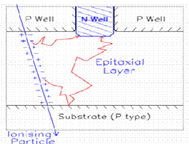
CMOS sensors are manufactured in standard CMOS technology, which offers low fabrication costs and fast turn-over for their development. The key element of this technology is the use of an n-well/p-epi diode to collect, through thermal diffusion, the charge generated by the impinging particle in the thin epitaxial layer (typically 5-15 µm, mostly undepleted) underneath the read-out electronics (see figure 1). The signal charge is thus proportional to the epitaxial thickness (~ 80 e--h pairs / µm for minimum ionizing particle – m.i.p.).
Figure 1: Detection principle of a Minimum Ionizing Particle going trough a CMOS sensor.
A peculiarity of the sensors is that they allow fabricating System-on-Chips (SoC) by integrating signal processing micro-circuits (amplification, pedestal correction, digitisation, sparsification, etc.) on the detector substrate. Moreover, the latter may be thinned down to a few tens of microns since the active volume is less than 20 µm thick. CMOS sensors thus present an attractive trade off between granularity, material budget, read-out speed and radiation tolerance, making them particularly well suited for the ILC-VD application.
2.2. Performances achieved with MIMOSA chips
The development of CMOS sensors for charged particle tracking was pioneered in Strasbourg in 1999 [3],[4],[5],[6]. The first years of the development allowed demonstrating that this technology provides excellent detection efficiency and spatial resolution. Furthermore, these results were also established with a macroscopic detector element.
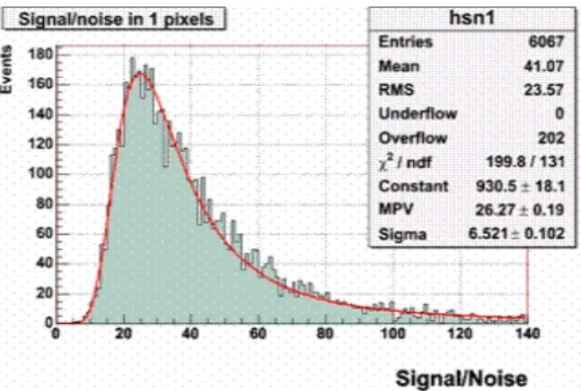
Most of the fabricated chips have been tested with m.i.p. (~120 GeV pion beam at the CERN-SPS, or ~5 GeV e- beam at DESY) demonstrating a typical Signal-to-Noise ratio (S/N) of ~ 20-30 (MIMOSA 9, 11, 14 in AMS 0.35 opto, figure 2), a spatial resolution of σsp ~ 1.5 µm (MIMOSA 1, 5 and 9 with a 20 µm pitch, figure 3), a detection efficiency (εdet) of ~ 99-99.9 % (even at temperatures near 40oC in the case of MIMOSA 9 and 11), and a double hit separation power (σ2hits) of ≥~ 30 µm.
2.3. Exploration of fabrication processes
The capability of developing radiation tolerant and fast sensors depends on basic fabrication parameters such as the epitaxial layer, the feature size, the number of metal layers, the leakage current, the doping and depth of the n- and p-wells, the oxide thickness, a.s.o., which may vary substantially from one fabrication process to another. Finding well adapted fabrication processes, which allow integrating the necessary signal conditioning micro-circuits in the sensor, with low pixel noise and pixel-to-pixel dispersion, is therefore a must. 13 MIMOSA chips have been designed and fabricated exploring 6 different fabrication processes: AMS-0.6µm,
AMI-0.35µm, AMS-0.35µm (opto and high-res), IBM-0.25µm, TSMC-0.25µm.
Figure 2: Typical Signal/Noise distribution for MIMOSA 9 prototype. (pitch = 20 µm; diode size = 14.62 µm2; temp. = 0oC)
Figure 3: Spatial resolution (µm) versus pixel size (µm) (MIMOSA 9 prototype, temperature = 0oC).
Among them, the AMS 0.35 opto process allowed realizing prototypes (MIMOSA 9 and 11) with the best detection performances [7]. These very satisfactory results were obtained because the noise of the pixels could be kept near 10 e- ENC. The induced comfortable S/N value translates into a detection efficiency exceeding 99.5 % even in the case of a large pitch (40 µm in MIMOSA 9) where charge collection is expected to eventually exhibit inefficiencies due to the sizeable path achieved by some charge carriers until the sensing diode. These results allow foreseeing a variable pitch for the vertex detector, ranging from 20 µm for the inner most layer to 40 µm for the outer layer, which translates into a reduced data flow and power dissipation.
3.Constraints from beamstrahlung background
3.1. Estimate of the beamstrahlung rate
The knowledge of the rate of beamstrahlung electrons traversing each detector layer deserves much attention since its magnitude dictates the necessary read-out speed (due to occupancy) and dominates the radiation tolerance requirements.
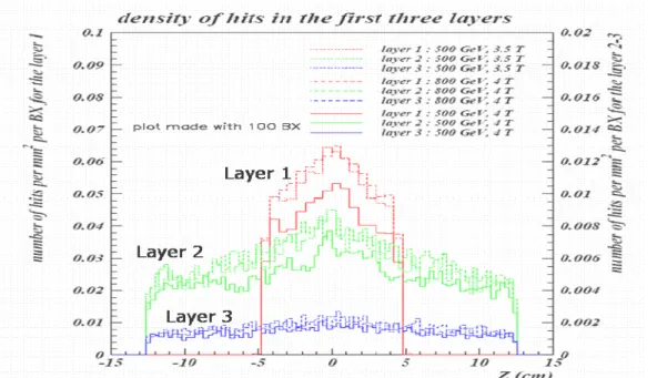
The electron rate has been reevaluated w.r.t. the TESLA TDR estimates, which were based on a single bunch crossing (BX), with the GUINEAPIG program [8]. Figure 4 summarises the results obtained with 100 BX and shows the hit density (hits/mm2/BX) along the direction parallel to the beam axis. One observes that the hit density in the inner most layer varies from about 3 hits/cm2/BX at the acceptance edges to more than 5 hits/cm2/BX near the vertical to the interaction point. This sizeable difference is due to ~10 MeV electrons produced close to 90o and traversing a large number of times (> 10) the inner most layer while they spiral in the 4 T magnetic field of the apparatus. The momenta of beamstrahlung electrons reaching the detector concentrate near 9-10 MeV/c. The hit rate decreases therefore rapidly with increasing radius: it is ~8 times smaller in the second layer and is still ~3 times smaller in the third layer.
However, the rates shown are subject to
uncertainties or unknowns which need to be considered when deriving constraints on the vertex detector performances. For instance, the rates increase by ~20 % if the experimental magnetic field happens to be of 3.5 T only, or if the collider is run at a collision energy of 800 GeV instead of 500 GeV. Moreover, the very limited accuracy of the generator should be taken into account, since the electrons of concern are at the edge of the phase space and since the process generation is still to be confronted to real data (the ILC will presumably provide the first opportunity for such a comparison). It is mandatory to take this uncertainty into account in the required detector performances. A global safety factor of 3 was chosen for this purpose, to apply on the raw Monte-Carlo output.
The hit density at 90o can therefore be estimated to possibly reach ~15 hits/cm2/BX. This upper limit determines the conditions in which the vertex detector should still be fully operational.
3.2. Consequences on the signal processing electronics
Accounting for the cluster multiplicity (~5-10) and the hit density uncertainty, a 50 µs read-out time for the first layer (as mentioned in the TESLA TDR) would hardly suffice to keep the occupancy under a few percent level.
Figure 4: Distribution of beamstrahlung hits in the three inner layers of the vertex detector along the direction parallel to the beam axis.
The target value was therefore fixed to ~≤ 25 µs, which is still not comfortable, but reflects a compromise which accounts for power dissipation, material budget and detector design considerations.
Moreover, a very valuable back-up for handling the occupancy in the inner most layer may come from the ~ 8 times lower hit density in the second layer: it will consist in extrapolating the track elements reconstructed in the four - much less crowded - outer layers down to the inner most layer. In case the occupancy turns out to be very high in the latter, the hits of interest can be selected by requiring them to be associated to a track element extrapolated from the other layers. This forces however the integration time to be significantly below 100 µs in the second layer (the TESLA TDR value was 250 µs). A target value of ~50 µs was retained for this purpose.
Since the hit density in the third layer is more than 20 times lower than in the inner most layer, a read-out time of ~≤200 µs can be considered as appropriate. The same target value was retained for the fourth and fifth layers, where the hit density is even lower.
4.Specific aspects of the CMOS VD concept
The detector concept taking best advantage of the CMOS sensor peculiarities with respect to other technologies, is likely to rely on a geometry similar to the one described in the TESLA TDR (based on CCDs).
It consists of 5 cylindrical layers with radii ranging from 15 to 60 mm. Depending on the layer, the polar angle coverage extends to |cosθ| ~ 0.90 - 0.95. A sideview of the detector geometry is shown in figure 5.
Figure 5: Side view of the detector geometry.
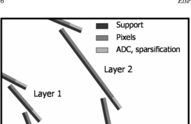
The fact that the columns are oriented perpendicular to the beam lines allows making them short enough to guarantee a swift read-out of the layers most exposed to the beamstrahlung electrons, even if their rate happens to be significantly higher than predicted by present simulations. The functionalities (ADC, sparsification and signal transfer electronics) which cannot be integrated in the pixels are located in a narrow band on the edge of the sensors (figure 6). The loss in resolution on the impact parameter derived from the study is modest (a few % [8]). Overall, the multiple scattering parameter b, entering into the canonical expression of the impact parameter resolution, increases by only ~5-10%, mainly because the material of the beam pipe governs the value of b, which grows essentially like the square root of the fraction of radiation length. In comparison, the benefit in read-out time is rather significant. For instance, shortening the read-out time from 50 of 25 µs allows reducing the radius of the inner most layer by ~ 15-20%. Since b is proportional to this radius, it decreases by the same amount.
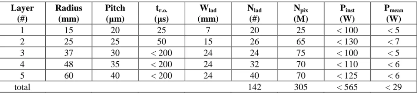
Layer (#) Radius (mm) Pitch (µm) tr.o. (µs) Wlad (mm) Nlad (#) Npix (M) Pinst (W) Pmean (W) 1 15 20 25 7 20 25 < 100 < 5 2 25 25 50 15 26 65 < 130 < 7 3 37 30 < 200 24 24 75 < 100 < 5 4 48 35 < 200 24 32 70 < 110 < 6 5 60 40 < 200 24 40 70 < 125 < 6 total 142 305 < 565 < 29
Table 1: Main features of the detector concept based on CMOS sensors. For each layer, the table indicates the radius, the pixel pitch, the read-out time, the ladder width, the number of ladders, the number of pixels, the instantaneous and average power dissipation.
Figure 6: Transverse view of layer 1 and 2 (the thickness is not at the real scale).
Prominent characteristics of the VD are summarised in table 1. The main differences with the TESLA TDR geometry include a faster read-out (and thus a larger number of ladders equipping the inner layers), a variable pixel pitch (and therefore a smaller total number of pixels: 300 millions instead of 800 millions, translating into a reduced data flux and power dissipation), less material at small polar angle, and the absence of a cryostat.
On the first layer, the pixels are grouped in columns of 256 units, read out in parallel at an effective clock frequency of ~ 10 MHz, which translates into a column read-out time of ~ 25 µs. The 2nd layer is designed with the same approach. On the other hand, the 3 outer layers, taking advantage of the much smaller data flux and of the long time between each train (~200 ms), rely on a different strategy. First, charge is sampled and stored inside a memory cell in the pixel during the beam train (about 5 memory cells per pixel are foreseen). Secondly, all cells are read out after the end of each bunch train (see section 7).
Another important issue concerns the power dissipation, mainly governed by the number of columns. For the whole detector, the expected instantaneous power dissipation would amount to ~550 W, a value which would still require substantial cooling. As for any of the technologies envisaged for the vertex detector, the crucial question arises on how well the beam time structure can be exploited to switch off (most of) the detector in between trains, or nearly so. A conservative approach was chosen for the present estimates, which assumes that the detector can be switched off (or nearly so) for at least 95 % of
the time, a hypothesis which translates into an average dissipation of ~ 30 W. This value is still considered as being compatible with a light cooling system.
The optimal operating temperature of the sensor is still to be found. Several different sensor prototypes have provided excellent detection performances while operated at room temperature. It may however be wise to run the detector at controlled temperature in order to reduce the sensitivity of the sensors to unexpected radiation effects, such as the rise of the electronic noise. It seems likely that this operating temperature will be compatible with a very light cooling system.
5.Issue of radiation tolerance
5.1. Radiation level expected
Taking into account the radiation level given by the new beamstrahlung studies and assuming that the sensor performances should remain essentially unchanged after 3 years of operation, the radiation tolerance requirements are based on a total electron flux of ~5.4x10¹² hits/cm2 [8]. The required radiation tolerance amounts therefore to ~150 kRad (including a safety factor of 3).
The non-ionising radiation level was estimated, assuming a NIEL factor of 30 for electrons of about 10 MeV [9],[10]. The expected fluence is about ≤2x10¹¹ n
eq/cm2 for 3 years of operation. This value is significantly larger than the expected fluence induced by the neutron gas circulating inside the experimental apparatus (~≤1010 n
eq/cm2/yr) 3.
5.2. Tolerance to 1 MeV neutrons and 10 MeV electrons
Recently, several sensors were irradiated with various types of particles in order to check that the neutron gas and the beamstrahlung electron doses ———
3 This value includes a safety factor of 10 applied to the output of Monte-Carlo simulations.
expected at the ILC are affordable. The chips were in particular exposed to ~ 1 MeV neutrons, 10 keV X-Rays and 9.4 MeV electrons.
A preliminary analysis of the data collected with the MIMOSA-9 chip exposed to a fluence of 1x10¹²neq/cm2 shows that the detection efficiency remains essentially unaffected, staying around 99.5 % at an operating temperature of -20oC. This observed tolerance is much superior to the performance required for the ILC.
MIMOSA-9 and -5 chips were exposed to integrated doses of up to 1x10¹³e-/cm2. The preliminary results show that (at a temperature of -20oC) the S/N value is still high (~23 instead of ~28 before irradiation), and that the detection efficiency, which amounts still to 99.3±0.1%, changes only marginally.
The radiation tolerance studies performed in the last two years have established quite reliably that CMOS sensors can stand the ionising and non-ionising radiation doses to which the vertex detector is going to be exposed at the ILC, even if these doses come out to be much higher than the present Monte-Carlo predictions. This statement is however only fully valid if the sensors are operated at negative temperatures, typically about -10oC.
6.Issue of thinning
6.1. General remarks
The thickness ambitioned is ~50 µm and, if possible, twice less. While thinning sensors to ~50 µm is not expected to be particularly difficult or suspected to affect the sensor performances, a thickness of nearly 20 µm is considered as a challenge. The ability of industry to achieve it with a satisfactory yield needs to be assessed. Moreover, internal mechanical stress may occur, translating into wrinkling of the chip. The answer to this side effect may consist in gluing the chip on a thin carbon foam, diamond or beryllium support, which would ensure the necessary rigidity. A dedicated research effort has started, which ought to encompass bonding issues, to investigate such possibilities. It profits from similar
studies performed for the STAR upgrade and - eventually – for the CBM experiment at GSI.
6.2. Achieved thickness
It is now established since a few years that reticle size chips (i.e. MIMOSA-5) can be thinned down by industry to 120-130 µm, without any noticeable side effect. This is still 2.5 times too much for the resolution ambitioned on the track origin. Attempts were made to thin MIMOSA-5 sensors down to ~50 µm, guided by the development for the STAR vertex detector via collaborators from LBNL. The procedure was applied to individual, diced, sensors. The thinned sensors were bonded to a prototype ladder using a 50 µm thin film adhesive at LBNL. Up to 9 chips were mounted on a single ladder. Preliminary test results show that the bonding technique is efficient and that the sensor functionalities tested are all preserved.
More recently, another company, located in Europe, was contacted and has accepted to thin MIMOSA-5 chips to 50 ± 5 µm. The thinning of the first wafers is currently under way.
In conclusion, the procedure allowing thinning down the sensors to ~50 µm is still not fully established, but seems in good shape. Moreover, a more aggressive goal, such as 25 µm, may be accessible on the mid-term.
7.Issue of read-out speed
7.1. R & D on signal processing architecture
The design of the signal processing micro-circuits is strongly influenced by the need to cope with the large flux of beamstrahlung e- in the inner most layer. Since this flux decreases rapidly with increasing radius, a different architecture is envisaged for the outer layers, which takes advantage of the beam time structure. The following strategies are pursued to meet the running condition requirements: a massively parallel architecture with on-chip data sparsification adapted to the inner layers; for the outer layers, on-pixel storage for ~ 5 snapshots during a single bunch train crossing, the signal transfer and processing being postponed to the end of the train.
7.2. Present achievements
Since 2002, three different prototypes (MIMOSA-6, 7, 8) were fabricated in order to explore various charge collection and signal treatment architectures integrated in sensors adapted to fast, massively parallel, readout. These architectures are based on the concept of pedestal subtraction inside each pixel (via correlated double-sampling) and on grouping the pixels in short columns read out in parallel, each column being equipped with a single discriminator handling the signals coming out sequentially from all pixels of the column.
MIMOSA-8 [11] is the most recent prototype of this series. Its tests with a 55Fe source provide particularly encouraging results. It features in-pixel amplification and CDS, and is organized in 4 sub-arrays of 32 columns read out in parallel. Each column contains 32 pixels (25 µm pitch) and is ended with a discriminator. Preliminary results show that the noise levels are in the order of ~ 13-18 e-ENC, depending on the sub-array, and that the charge-to-voltage conversion gain is of ~ 50-70 (resp. 110) µV/e- for the different DC-coupling (resp. AC-coupling) architectures. Moreover, the pixel-to-pixel dispersion comes out to be particularly low and matching the requirements.
8.Summary
The R&D on CMOS sensors for the ILC vertex detector has made significant progress. The beam background has been evaluated with improved accuracy, leading to substantially more severe radiation tolerance and read-out speed requirements.
A preliminary vertex detector design has been proposed, taking into account the peculiarities and advantages of the CMOS sensors. It assumes two different read-out architectures: a fast one, based on column parallel processing, adapted to layer 1-2 and another one, relying on memory cells integrated in each pixel, adapted to layer 3-5. The development of the fast column parallel architecture is well advanced. The radiation tolerance of the sensors to 1 MeV neutrons and 9 MeV electrons was investigated and found sufficient for the expected background rates. Finally, the thinning procedure has made headway down to 50 µm.
The coming years will be dedicated to consolidate the detector concept, the thinning procedure, the power consumption, and the fast read-out architectures. The latter will include a major outcome on a fast ADC (~ 4-5 bits) integrated in the side band at the end of each column, on a reticle size prototype. Besides the effort devoted to the design of the sensors adapted to the inner layers, a prototype (called MIMOSA-12) adapted to the outer layers was designed and sent for fabrication by the end of March 2005. It features 4 capacitors inside each pixel. The latter have a pitch of 35 µm. The sensor includes 6 different sub-arrays exploring various MOS capacitors (50, 100 and 200 fF). A major issue of this type of design consists in finding the smallest possible capacitors in order to integrate the largest possible number of them in each pixel.
Finally, the characteristics of processes providing a feature size below 0.25 µm will be investigated. These efforts should allow the CMOS sensors to become more and more likely to fulfill the detector performance requirements.
References
[1] TESLA Technical Design Report
http://tesla.desy.de/new_pages/TDR_CD/start.html [2] M.Winter. "Looking forward: a detector for the future Linear
Collider machine" IEEE Trans.Nucl.Sci., (2004). [3] A list of all fabricated prototypes can be found here:
http://ireswww.in2p3.fr/ires/recherche/capteurs/list/list.html [4] R.Turchetta et al. Nucl.Instr.Meth. A458 (2001), 677. [5] G. Deptuch at al. “Design and Testing of MAPS…” IEEE
Trans.Nucl.Sci., Vol. 49, No 2, (2002), 601.
[6] G. Deptuch et al. “Development of MAPS for charged particle tracking”, Nucl.Instr.Meth., A511 (2003), 204.
[7] W. Dulinski et al. “Optimization of Tracking Performance of CMOS…”, in proceedings of IEEE NSS-MIC 2004, Oct. 12-22, Rome, Italy, accepted for Transaction on Nuclear Science. [8] http://www.desy.de/f/prc/docs_rd/prc_rd_01_04_update_02_0
5.pdf A.Besson et al. DESY PRC R&D NR 01/04 (2005) [9] A. Vasilescu. “The NIEL scaling hypothesis…”, ROSE coll.
Preprint TN/97-2 (revised Dec.99) and references therein. [10]G.P. Summers et al.. IEEE Trans. Nucl. Sci. NS-40 (1993),
p.1372.
[11]Y. Degerli et al. “A Fast Monolithic Active Pixel Sensor …”, in proceedings of IEEE NSS-MIC 2004, October 12-22, Rome, Italy, accepted for Transaction on Nuclear Science.