Beam Alignment and Image Metrology for
Scanning Beam Interference
Lithography–Fabricating Gratings with
Nanometer Phase Accuracy
by
Carl Gang Chen
B.A., Swarthmore College (1995)
S.M., Massachusetts Institute of Technology (2000)
Submitted to the Department of Electrical Engineering and Computer
Science
in partial fulfillment of the requirements for the degree of
Doctor of Philosophy
at the
MASSACHUSETTS INSTITUTE OF TECHNOLOGY
June 2003
c
° Massachusetts Institute of Technology 2003. All rights reserved.
Author . . . .
Department of Electrical Engineering and Computer Science
May 23, 2003
Certified by . . . .
Mark L. Schattenburg
Principal Research Scientist, MIT Center for Space Research
Thesis Supervisor
Accepted by . . . .
Arthur C. Smith
Chairman, Department Committee on Graduate Students
Beam Alignment and Image Metrology for Scanning Beam
Interference Lithography–Fabricating Gratings with
Nanometer Phase Accuracy
by
Carl Gang Chen
Submitted to the Department of Electrical Engineering and Computer Science on May 23, 2003, in partial fulfillment of the
requirements for the degree of Doctor of Philosophy
Abstract
We are developing a scanning beam interference lithography (SBIL) system. SBIL is capable of producing large-area linear diffraction gratings that are phase-accurate to the nanometer level. Such gratings may enable new paradigms in fields such as semi-conductor pattern placement metrology and grating-based displacement measuring interferometry. With our prototype tool nicknamed “Nanoruler”, I have successfully patterned, for the first time, a 400 nm period grating over a 300 mm-diam. wafer, the largest that the tool can currently accommodate.
By interfering two small diameter Gaussian laser beams to produce a low-distortion grating image, SBIL produces large gratings by step-and-scanning the photoresist-covered substrate underneath the image. To implement SBIL, two main questions need to be answered: First, how does one lock the interference image to a fast-moving substrate with nanometer accuracy? Secondly, how does one produce an interference image with minimum phase nonlinearities while setting and holding its period to the part-per-million (ppm) level? My thesis work solves the latter problem, which can be further categorized into two parts: period control and wavefront metrology.
Period control concerns SBIL’s ability to set, stabilize and measure the image grating period. Our goal is to achieve control at the ppm level in order to reduce any related phase nonlinearity in the exposed grating to subnanometers. A grating beamsplitter is used to stabilize the period. I demonstrate experimental results where the period stabilization is at the 1 ppm level. An automated beam alignment system is built. The system can overlap the beam centroids to around 10 µm and equalize the mean beam angles to better than 2 µrad (0.4 arcsec), which translates into a period adjustability of 4 ppm at 400 nm. Image period is measured in-situ via an interferometric technique. The measurement repeatability is demonstrated at 2.8 ppm, three-sigma. Modeling shows that such small period measurement error does not accumulate as growing phase nonlinearities in the patterned resist grating; rather, the resist grating has an averaged period that equals the measured period. Any phase nonlinearity is periodic and subnanometer in magnitude.
SBIL wavefront metrology refers to the process of mapping the phase of the grating image and adjusting the collimating optics so that minimum image phase nonlinearity
can be achieved. The current SBIL wavefront metrology system employs phase shift-ing interferometry and determines the image nonlinearity through a moir´e technique. The system has an established measurement repeatability of 3.2 nm, three-sigma. I am able to minimize the nonlinearity to 12 nm across a 2 mm-diam. image. Mod-eling shows that despite an image phase nonlinearity at the dozen nanometer level, printed phase error in the resist can be reduced to subnanometers by overlapping scans appropriately.
From the point of view of period control and wavefront metrology, I conclude that SBIL is capable of producing gratings with subnanometer phase nonlinearities. Thesis Supervisor: Mark L. Schattenburg
Acknowledgments
More than half of this dissertation was written in Beijing, China, at my parents’ place over the course of six months, from September 2002 to February 2003. Little did I anticipate that the anti-terrorism campaign would have such a profound impact on my own life, and on the lives of so many other foreign students. Fortunately, given the circumstances, I was stuck at the right place: home. In hindsight, the forced exile might have been one of the best things that happened to me. I am stronger because of it.
During those six agonizing months, I had the love and support of my family and friends to count on. To them, I am forever grateful. Special thanks go to Paul Konkola, Ralf Heilmann, Chulmin Joo, Raymond Scuzzarella, Craig Forest, Yanxia Sun, Juan Montoya, Ed Murphy, Bob Fleming and Mark Schattenburg. They man-aged to ship a hundred kilograms of notebooks, data and references to me, without which, there would not have been any thesis. Another special thank-you to Fred Gevalt, the person who braved the bureaucracy and managed to get me back in time so that I can put an appropriate end to my MIT career.
I have the honor to be the first student who did both his Master’s and PhD under the guidance of Dr. Schattenburg. Mark is an effective yet easy-going advisor. I can express and argue my ideas freely in front of him. I am very grateful to his continuing financial support during my time in China. His questions and suggestions have significantly enhanced the quality of my work.
Paul’s skill in controls and mechanical design is enviable. As the only people working full time on SBIL (until I was held up in China), he and I have collaborated closely over the years. I am honored to call him a dear colleague and a loyal friend. One could only hope that the camaraderie will last a lifetime.
Ralf contributed considerably towards SBIL research by designing and implement-ing the phase measurement optics used for heterodyne frimplement-inge lockimplement-ing. I also deeply appreciate his help in taking some new period measurement data so that I could analyze them in Beijing and report the findings at a conference.
With every passing day, Chulmin is a step closer to realizing his dream of becoming a MIT PhD. I wish him the best of luck, and may I remind the man that he still owes me a dinner in Seoul. I am proud to have Craig as a friend. His enthusiasm and warmth are refreshing. Yanxia has been working extremely hard since she joined the team. I wish her some joyful downtime in the coming year. Over the past couple of months, Juan has become a good colleague and friend. He is starting to put his
own signature on the SBIL project. Bob’s caring for the lab made it not-too-painful a place to spend 24 hours in. His good sense of humor is most memorable. Captain Ed’s mastery of fab-processes makes him invaluable to my work. He is easily one of the nicest follows that I know. I wish him the best. Not enough thank-you’s can express my gratitude towards Ray, whose help during my time of need can most certainly be counted on. As new members, Chih-Hao Chang and Mireille Akilian have demonstrated their skills convincingly. The future of SNL looks bright because of them.
I thank Professors Henry Smith and Cardinal Warde for serving as my thesis readers. I benefitted from their questions.
The work documented in this dissertation is done at the MIT Space Nanotechnol-ogy Laboratory, and is supported by grants from NASA and DARPA.
Contents
1 Introduction 27
1.1 Mechanically-ruled gratings . . . 28
1.2 Interference gratings . . . 29
1.3 Gratings for new paradigms . . . 30
1.4 Scanning beam interference lithography . . . 33
1.4.1 Interference lithography at MIT . . . 33
1.4.2 SBIL concept . . . 37 1.4.3 System advantages . . . 39 1.4.4 System overview . . . 39 1.4.5 Patterned gratings . . . 50 2 SBIL optics 53 2.1 Introduction . . . 54 2.1.1 Grating beamsplitter . . . 54 2.1.2 Optics . . . 55
2.1.3 Thin lens equation for Gaussian beams . . . 56
2.2 Optical design and layout . . . 58
2.2.1 Lithography interferometer . . . 58 2.2.2 Spatial filtering . . . 61 2.2.3 Beamsplitter mode . . . 66 2.2.4 Lithography mode . . . 68 2.2.5 Grating mode . . . 68 2.3 Summary . . . 69 3 Beam alignment 71 3.1 Theory . . . 72
3.1.1 Beam position and angle decoupling . . . 73
3.1.2 Angle PSD placement error . . . 75 9
10 CONTENTS
3.1.3 Iterative beam alignment . . . 77
3.2 System setup . . . 80
3.2.1 Beamsplitter mode . . . 80
3.2.2 Rectangular beamsplitter design, installation and non-ideality 84 3.2.3 Beam overlapping PSD . . . 89
3.2.4 Grating mode . . . 90
3.3 Noise study . . . 92
3.3.1 Digitization noise floor . . . 92
3.3.2 DAQ system accuracy . . . 93
3.4 Period stabilization . . . 95
3.4.1 Experimental setup . . . 96
3.4.2 Measurement consistency . . . 97
3.4.3 Angular noise correlation . . . 97
3.5 Results . . . 101
3.5.1 Beam position and angle instabilities . . . 101
3.5.2 Beam alignment performance . . . 104
3.6 Summary . . . 106
4 Period measurement 107 4.1 Theory . . . 109
4.1.1 Principle of operation . . . 110
4.1.2 Point detector without beam diverting mirror . . . 114
4.1.3 Point detector with beam diverting mirror . . . 117
4.1.4 Measurement error for a point detector . . . 123
4.1.5 Wave model for a non-point detector . . . 124
4.1.6 Locations of Gaussian beam centroids . . . 126
4.1.7 Period measurement with a non-point detector . . . 129
4.1.8 Measurement error for a non-point detector . . . 133
4.1.9 Period measurement with a pseudo-ideal beamsplitter . . . 134
4.1.10 Period measurement with a non-ideal beamsplitter . . . 141
4.1.11 Fringe nonlinearity-induced stitching error . . . 150
4.1.12 Summary . . . 152
4.2 Error modeling . . . 153
4.2.1 Fringe counting . . . 153
4.2.2 Noise sensitivity . . . 156
4.2.3 The model . . . 156
CONTENTS 11
4.2.5 Stage displacement error . . . 159
4.3 System setup and experimental procedure . . . 159
4.4 Results . . . 161
4.4.1 Low-pass digital filter design . . . 161
4.4.2 Period measurement . . . 164
4.5 Phase error in the resist grating . . . 168
4.6 Summary . . . 176
5 Wavefront metrology 177 5.1 Introduction . . . 177
5.2 Theory . . . 180
5.2.1 Moir´e phase . . . 180
5.2.2 Scalar Gaussian beam . . . 181
5.2.3 The q transforms . . . 183
5.2.4 The model . . . 183
5.2.5 Coordinate transformations . . . 185
5.2.6 Simulated moir´e phase maps . . . 186
5.2.7 Action of the focusing lens . . . 192
5.2.8 Phase nonlinearity due to beam angle variations . . . 194
5.2.9 Observation of the moir´e pattern (I) . . . 199
5.2.10 Observation of the moir´e pattern (II) . . . 202
5.2.11 The use of collimating optics . . . 204
5.2.12 The metrology grating . . . 209
5.2.13 Summary . . . 209
5.3 Phase shifting interferometry . . . 210
5.3.1 PSI vs. single-interferogram analysis . . . 210
5.3.2 Phase unwrapping . . . 212
5.3.3 The Hariharan five-step algorithm . . . 213
5.3.4 Computer simulation of the interferograms . . . 216
5.4 System setup . . . 216
5.4.1 Optics placement requirements . . . 216
5.4.2 System layout . . . 217
5.4.3 Experimental procedure . . . 217
5.4.4 Hardware . . . 219
5.5 Results . . . 221
5.5.1 Beam diameter . . . 221
12 CONTENTS
5.5.3 Minimization of the nonlinear phase . . . 226
5.5.4 Lens aberrations . . . 226
5.5.5 Theory vs. experiment . . . 228
5.6 Printed phase error . . . 231
5.7 Numerical artifacts and dose contrast . . . 239
5.8 Summary . . . 243
6 Conclusions 245 A Recipe for writing 300 mm wafers 249 B Fringe period stabilization via a grating beamsplitter 251 C Drawings for installing and aligning the rectangular beamsplitter 253 D Period measurement with a conventional cube beamsplitter 259 E Mathematics on intensity integration during period measurement 263 F MATLAB scripts for resist-grating phase simulations 265 F.1 RGP.m . . . 265
F.2 ShiftAdd.m . . . 268
G MATLAB scripts for wavefront metrology simulations 269 G.1 WaistLoc.m . . . 269
G.2 InvRphi.m . . . 270
G.3 Moir´e.m . . . 271
List of Figures
1-1 A reflection grating. Schematic only. . . 28 1-2 Chart adapted from the 2002 Update of the International Technology
Roadmap for Semiconductors (ITRS). The first row gives the year of the device generation and the second indicates the target minimum feature size–as is customary DRAM half-pitch is used. The third row indicates the allowed CD variation. The fourth gives the wafer overlay tolerance, and the fifth is an estimate of the necessary metrology tool accuracy, taken to be one-ninth of the overlay error. . . 31 1-3 Two accurate gratings enable in-situ measurement of the objective-lens
distortion in a stepper via a moir´e technique. Schematic only. . . 32 1-4 A displacement measuring grating interferometer used to control a
rul-ing engine. The reflection gratrul-ing has half the spatial frequency of the transmission grating. The reflection grating is used at §2-orders whereas the transmission grating at zero and first order. One fringe cycle observed at the detector corresponds to a relative displacement of one-quarter the period of the reflection grating. . . 33 1-5 During interference lithography, the nominal fringe period p at the
substrate is determined by the beam incident angles θ1 and θ2, and the
laser’s wavelength λ. . . 34 1-6 A schematic diagram of the traditional interference lithography system
at MIT. . . 35 1-7 Nonlinear phase distortions due to the interference of two spherical
waves with 1 m wavefront radii, assuming that the system is in perfect alignment and is set up for a nominal grating period of 400 nm. (a) The interference coordinates. (b) Phase discrepancy from an ideal linear grating. The region with subnanometer nonlinear phase is less than 2.8 mm in diameter. . . 36 1-8 Scanning beam interference lithography system concept. . . 38
14 LIST OF FIGURES
1-9 SBIL step-and-scan scheme. (a) Top view. The step and scan direc-tions are x and y, respectively, which are also defined in Figure 1-8. To ensure good stitching between adjacent scans, the stage must step over by an integer number of fringe periods. (b) Gaussian intensity envelope of one scan. Period exaggerated. (c) Beam overlapping to create a uniform exposure dose. . . 38 1-10 SBIL system, front view. Currently configured to write 400 nm period
gratings. The whole system is housed inside a Class 10 environmental chamber. . . 41 1-11 SBIL system, back view. Continued from Figure 1-10. . . 42 1-12 SBIL environmental enclosure. (a) External view. (b) Internal view
with air flow paths outlined. All major thermal sources, which include the HeNe stage interferometer laser and all three acousto-optic mod-ulators (AOMs), have been enclosed. Heat is actively pumped away from the optical bench via ducts. . . 43 1-13 SBIL lithography and metrology optics. . . 45 1-14 SBIL lithography and grating reading modes. Schematic only. (a)
Lithography mode. By setting the frequencies to the acousto-optic modulators (AOM) and combining the appropriate diffracted beams, one generates two heterodyne signals at phase meters (PM) 1 and 2. A digital signal processor (DSP) then compares the signals and drives AOM2 to keep the phase difference between the two arms constant. (b) Grating reading mode. A grating is used in the so-called Littrow condition, where the 0-order reflected beam from one arm coincides with the -1-order back-diffracted beam from the other arm. Two het-erodyne signals, PM3 and PM4, differ in the sense that PM4 contains the spot-averaged phase information from the grating. . . 46 1-15 The monolithic beamsplitter design. Schematic only. Beam path
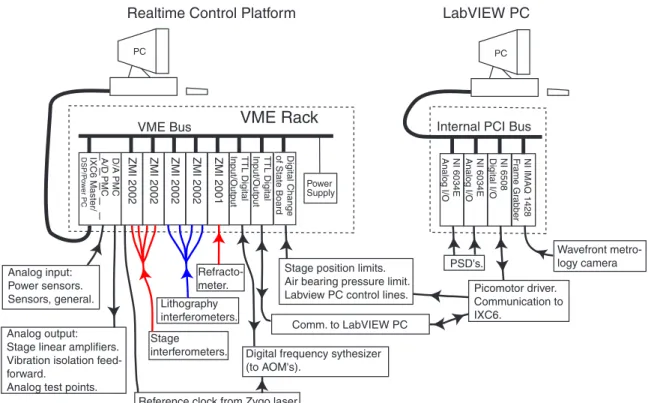
bend-ing due to refraction is not shown. . . 47 1-16 SBIL system architecture. The use of two separate platforms allows
parallel software and hardware development. . . 48 1-17 Photo showing the Super-Invar chuck and the Zerodur metrology block,
which together define the heart of the SBIL substrate and metrology frame. A 100 mm wafer with gratings can be seen on the chuck. . . . 49
LIST OF FIGURES 15
1-18 A scanning electron micrograph (SEM) of the cross section of a grat-ing written by SBIL. ARC is the acronym for anti-reflection coatgrat-ing. The resist, ARC and developer used are Sumitomo PFI-34 i-line resist, Brewer ARC-XL and Arch Chemicals OPD 262 positive resist
devel-oper, respectively. . . 51
2-1 (a) For a grating beamsplitter, beam angular variations along the x-direction are antisymmetrically correlated. The figure is schematic only. (b) For a cube beamsplitter, variations are symmetrically corre-lated. . . 54
2-2 Various physical parameters defining a Gaussian beam. The beam is propagating along the z direction. The beam irradiance varies along z and achieves a minimum at the beam waist. . . 57
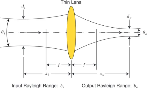
2-3 Transformation of a Gaussian beam by a thin lens. Beam size is exag-gerated. . . 57
2-4 Lens layout. For better illustration, the light path has been unfolded to a straight line. To write 400 nm period gratings, the beam must be incident upon the substrate at an angle of 26◦. . . 59
2-5 Drawing of the SBIL optics layout in the beamsplitter mode. . . 62
2-6 Drawing of the SBIL optics layout in the grating mode. . . 63
2-7 Drawing of beam paths in the beamsplitter mode. . . 64
2-8 Drawing of beam paths in the grating mode. . . 65
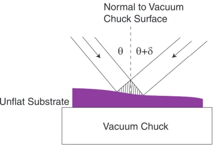
3-1 Fringe tilt results in phase error if the substrate is unflat. . . 72
3-2 Angle decoupling topology. . . 73
3-3 Position decoupling topology. . . 74
3-4 Position decoupling topology continued. . . 75
3-5 Design for a general beam alignment system. . . 77
3-6 Cartoon demonstrating the iterative beam alignment principle. The two-axis outputs from the position and angle PSDs are graphically represented as square boxes. Mirrors M1 and M2 are driven iteratively to zero the beam spots, marked by solid circles, in both position and angle to the desired locations, marked by crosses. Dashed lines circle the regions where the spots may lie in. . . 78
3-7 SBIL beam alignment system concept (beamsplitter mode). . . 81
16 LIST OF FIGURES
3-9 Four degrees of freedom defining each arm during the beamsplitter-mode alignment. . . 84 3-10 Rectangular beamsplitter design. . . 85 3-11 Rectangular beamsplitter design continued. Quality-control (QC) tests. 86 3-12 Rectangular beamsplitter shape distortions. . . 88 3-13 Photo of the vacuum chuck with the rectangular beamsplitter and the
beam overlapping PSD attached. The chuck is machined out of a single block of Super Invar, and is flat to within 1 µm. . . 89 3-14 Beam alignment in the grating mode does not necessarily guarantee
equal angles of incidence for the left and the right arms. It does guar-antee that the beams are on top of each other at the grating. . . 91 3-15 Digitization noise study. The A/D board is sampled at 100 kHz for
6 s while all six input channels dedicated to beam position and angle sensing are shorted. . . 93 3-16 Optical setup for determining the DAQ system accuracy. . . 94 3-17 DAQ system accuracy study. The DC-subtracted power spectral
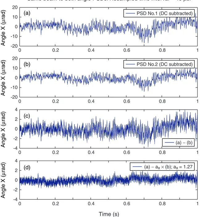
den-sity plots are averaged from five data sets. Each is 1 s long and sampled at 100 kHz. . . 95 3-18 Same beam–the right arm–onto both angle PSDs. (a) DC-subtracted
angle-x readout from Angle PSD No.1. (b) DC-subtracted angle-x readout from Angle PSD No.2. (c) Difference between a and b without gain adjustment. (d) Difference between a and b with gain adjustment. 98 3-19 Measurement consistency. The DC-subtracted power spectral density
plots for the angle-x and angle-y difference signals, averaged from 10 data sets. . . 99 3-20 Angular noise correlation along x. (a) Angle-x noise in the left arm,
and (b) in the right arm. (c) Gain adjusted sum of (a) and (b). . . . 100 3-21 Angular noise correlation along y. (a) Angle-y noise in the left arm,
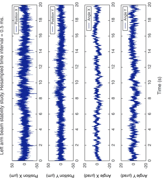
and (b) in the right arm. (c) Gain adjusted difference between (a) and (b). . . 100 3-22 A sample data set from the beam instability study for the left arm. All
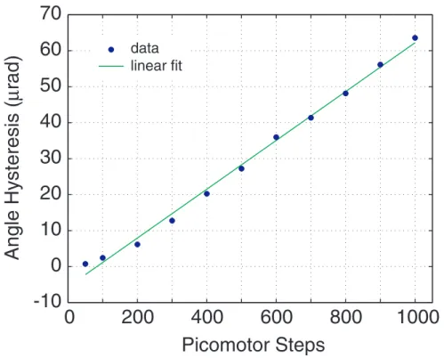
data are DC-subtracted. . . 103 3-23 Beam alignment results. . . 105
LIST OF FIGURES 17
4-1 Stitching scans. (a) The ideal case where the stage moves by an in-teger number of fringe periods. Contrast is optimal. (b) The worst case where the stage moves by an additional one-half of a fringe pe-riod. Contrast is completely lost. Fringe period grossly exaggerated for illustration. . . 108 4-2 Beamsplitter period measurement scheme. . . 109 4-3 Ray trace for the case where the point detector is fixed while the
beam-splitter is displaced by a distance D. The left and right incident angles are equal. . . 112 4-4 Ray trace for the case where the point detector and the beamsplitter
move together. The left and right incident angles are equal. . . 113 4-5 Ray trace for the case where the point detector is fixed while the
beam-splitter is displaced by a distance D. The left and right incident angles are not equal. . . 115 4-6 Period measurement with a common beamsplitter cube. The point
detector is fixed while the beamsplitter is displaced by a distance D. The left and right incident angles are not equal. Appendix D presents a detailed analysis. . . 116 4-7 Ray trace for the case where the point detector and the beamsplitter
move together. The left and right incident angles are not equal. . . . 118 4-8 Ray trace for the case where the point detector and the beamsplitter
move together. A beam diverting mirror is used. The rays have been unfolded to reveal the equivalence to Figure 4-7. . . 120 4-9 Ray trace for the case where the point detector is fixed while the
beamsplitter-mirror assembly moves. To be continued in Figure 4-10. 121 4-10 Ray trace for the case where the point detector is fixed while the
beamsplitter-mirror assembly moves. Continued from Figure 4-9. . . . 122 4-11 Wave model development. Optical path length changes are encoded as
planar wavefronts. . . 125 4-12 Ray trace showing the movements of the Gaussian beam centroids, for
the case where the photodiode is fixed while the beamsplitter-mirror assembly moves. To be continued in Figure 4-13. . . 127 4-13 Ray trace showing the movements of the Gaussian beam centroids, for
the case where the photodiode is fixed while the beamsplitter-mirror assembly moves. Continued from Figure 4-12. . . 128
18 LIST OF FIGURES
4-14 Ray trace showing the movements of the Gaussian beam centroids, for the case where the photodiode and the beamsplitter-mirror assembly move together. . . 130 4-15 An imperfect beamsplitter. (a) Interface tilt may develop as a result
of misalignment. (b) Tilt may also exist because of non-ideal optics manufacturing. . . 135 4-16 Period measurement with a pseudo-ideal beamsplitter. Ray trace
show-ing the OPL variations. To be continued in Figure 4-17. . . 136 4-17 Period measurement with a pseudo-ideal beamsplitter. Ray trace
show-ing the OPL variations. Continued from Figure 4-16. . . 137 4-18 Period measurement with a pseudo-ideal beamsplitter. Ray trace
show-ing the movements of the beam centroids. To be continued in Figure 4-19. . . 139 4-19 Period measurement with a pseudo-ideal beamsplitter. Ray trace
show-ing the movements of the beam centroids. Continued from Figure 4-18. 140 4-20 A non-ideal beamsplitter has both interface and surface tilts. . . 141 4-21 Period measurement with a non-ideal beamsplitter. Ray trace showing
the OPL variations. To be continued in Figures 4-22—4-26. . . 144 4-22 Period measurement with a non-ideal beamsplitter. Ray trace showing
the OPL variations. Continued from Figure 4-21. . . 145 4-23 Period measurement with a non-ideal beamsplitter. Ray trace showing
the OPL variations. Continued from Figure 4-21. . . 146 4-24 Period measurement with a non-ideal beamsplitter. Ray trace showing
the OPL variations. Continued from Figure 4-21. . . 147 4-25 Period measurement with a non-ideal beamsplitter. Ray trace showing
the OPL variations. Continued from Figure 4-21. . . 148 4-26 Period measurement with a non-ideal beamsplitter. Ray trace showing
the OPL variations. Continued from Figure 4-21. . . 149 4-27 Fringe counting. The period is exaggerated. Note that the figure shows
the oscillation envelope predicted by Eq. (4.49). The envelope is ob-served experimentally. . . 153 4-28 Fractional cycles, and related coordinates. . . 154
LIST OF FIGURES 19
4-29 Four schematic wave forms that may appear at the output of a pho-todiode during period measurement. Based on the numbers of peaks (np) and valleys (nv) present, one can classify them into three different
cases. Two fall under Case 3 where np = nv. The number of completed
cycles is Nm, which can be related to either np or nv. . . 155
4-30 Photo of the SBIL period measurement system. The angle PSD used for sensing the interference power signal is not pictured. Figure 2-6 should also be helpful. . . 160 4-31 Raw and digitally filtered period measurement data. p = 1.7644 µm. . 162 4-32 AC power spectral densities of the raw and digitally filtered data shown
in Figure 4-31. . . 163 4-33 Causal FIR low-pass filter design with a Kaiser window (M = 726, b
= 5.6533). Cutoff frequency is 70 Hz with a transition bandwidth of 10 Hz. . . 164 4-34 Causal FIR low-pass filter design with a Kaiser window (M = 1450, b
= 5.6533). Cutoff frequency is 250 Hz with a transition bandwidth of 10 Hz. . . 165 4-35 AC power spectral densities of the raw and digitally filtered data shown
in Figure 4-36. . . 165 4-36 Raw and digitally filtered period measurement data. p = 401.246 nm. 166 4-37 Experimental period measurement repeatability, derived from 16 data
sets. . . 167 4-38 Plot of the difference between φres and φm for the following simulated
parameters: number of scans = 40, actual grating image period p = 400 nm, measured grating image period pm= 400.0011 nm, percentage
measurement error ∆ = 2.8 ppm, 1/e2 intensity radius R = 1 mm, and
step size S = 0.9 mm. . . 170 4-39 Plot of the difference between φres and φm. Same parameters as those
used in Figure 4-38, except that the percentage measurement error is increased to 15 ppm. . . 171 4-40 Flexibility in setting the resist grating period. . . 172
20 LIST OF FIGURES
4-41 Dose contrast variations lead to grating line width variations. (a) Ideal case. Background dose BDcoincides with the resist clipping level. Dose
amplitude variations from AD to A0D do not have any impact on the
grating line width if 1:1 line-space ratio is desired. (b) If BD is not set
correctly, or if the clipping property of the resist varies with position, the line width changes depending on the dose amplitude. . . 173 4-42 Subplots (a) and (b) are the quantities E and F , respectively, which
together make up the total dose amplitude AtotD [Eq. (4.127)]. Subplots
(c) and (d) correspond to the total dose amplitude AtotD and the nominal
dose amplitude Atot
D,0 [Eq. (4.133)], respectively. The set of simulated
parameters is the same as that used in Figure 4-39. . . 174 4-43 Continued from Figure 4-42. Plot of the normalized dose amplitude
error eA. . . 175
5-1 SBIL wavefront metrology concept. (a) A metrology grating with an ideal linear spatial phase is used under the Littrow condition. The reflected and back-diffracted beams interfere at a CCD camera. (b) Two collimated Gaussian beams interfere at their waists and produce the grating image. Beam size is exaggerated. . . 179 5-2 The superimposition of two linear gratings gives rise to Moir´e fringes. 181 5-3 Setup geometry for one of the lithography arms. The collimating lens
is by assumption a thin lens. Beam size is exaggerated. . . 184 5-4 Coordinate frames describing the interference of collimated Gaussian
beams. Beam size is exaggerated. . . 186 5-5 The moir´e phase map when parameters in both arms are set to base
values (Table 5.1). . . 189 5-6 The moir´e phase map when z1R is at base value and z1L is increased
by 80 µm, i.e., the relative offset between the two collimating lenses is 80 µm. See Figure 5-4 for coordinate definitions. . . 189 5-7 The moir´e phase map when both z1L and z1R are increased from their
base value by 5 mm. . . 190 5-8 The moir´e phase map when z1R is increased by 5 mm and z1L by
5.08 mm, i.e., the relative offset between the two collimating lenses is 80 µm. . . 190 5-9 The moir´e phase map when dL is increased from its base value by
135 mm. . . 191 5-10 Spatial filter geometry. Beam size is exaggerated. . . 192
LIST OF FIGURES 21
5-11 A plot of j∆w0j and j∆z0j vs. j∆zij. Displacement of the focusing lens
affects the focused beam waist size and location. . . 193 5-12 The moir´e phase map when the initial beam waist radii at the pinholes,
w0L and w0R, are changed by ¡3 nm and +3 nm, respectively. . . 195
5-13 The moir´e phase map for a worst case study where the parameters w0L, w0R, dR, z1L and z1R are offset from their base values by ¡3 nm,
+3 nm, ¡10 mm, +5 mm and +4.92 mm, respectively. Again, the relative offset between z1L and z1R is 80 µm. . . 195
5-14 Beam angles during grating mode alignment. (a) Ideal case. (b) Non-ideal case. . . 196 5-15 The moir´e phase map produced with the same set of parameters as
in Figure 5-13, except angle variations are now included, with θL =
θ + ∆θ¡ δ and θR= θ¡ ∆θ + δ, where θ is the base value (Table 5.1),
∆θ = 250 µrad and δ = 11.4 µrad. . . 197 5-16 The moir´e phase map produced with the same parameter values as in
Figure 5-15, except now θL= θ + θerr+ ∆θ¡ δ, where θerr= 6 µrad. . 197
5-17 The moir´e phase map produced with all parameters set at base values, except θL, which is increased by 6 µrad. The linear phase shown is
due to the difference in period between the metrology grating and the grating image. . . 198 5-18 Light diffraction off a shallow sinusoidal reflection grating. . . 200 5-19 Observation of the moir´e fringes. Coordinate setup. . . 203 5-20 Moir´e phase maps observed at the CCD. (a) When the system is used
under the same condition that leads to Figure 5-15. (b) Under the same condition but with 6 µrad angle misalignment between the reflected and back-diffracted beams. . . 205 5-21 The inverse radius of curvature of a Gaussian wavefront as a function
of the propagation distance. . . 206 5-22 Geometric layout for Gaussian beam interference in the far field. The
focused beam waist radius at the pinhole is w0. The propagation
22 LIST OF FIGURES
5-23 (a) The maximum grating image phase discrepancy from an ideal linear grating as a function of the waist-to-substrate distance d. The wave-length of the laser is 351.1 nm. The nominal grating period is 200 nm. The 1/e2 grating image diameter is 2 mm. (b) The corresponding
initial beam waist radius w0 as a function of the waist-to-substrate
distance. See Figure 5-22 for parameter definitions. . . 208 5-24 Phase insensitivity as a function of the phase step. Least sensitivity
occurs at a phase step of π/2. . . 214 5-25 Photo of the SBIL wavefront metrology system. Study in conjunction
with Figures 1-13, 2-6 and 2-8. . . 218 5-26 Control block diagram for generating phase steps. . . 219 5-27 Plot of the phase discrepancy between an IL-exposed grating and a
perfect linear grating. The nominal grating period is 400 nm. Com-pared to Figure 1-7(b), the only changed parameters are dR= 995 mm,
dL= 1005 mm. . . 221
5-28 (a) Intensity distribution of the back-diffracted beam as recorded by the CCD. (b) Cross section of the intensity data in part (a) at y = 0, fitted with a Gaussian function. The fit shows that the 1/e2 beam diameter is approximately 1.92 mm, or 286 pixels. . . 222 5-29 A sequence of five moir´e intensity images, with π/2 rad phase shift
between adjacent frames. The moir´e phase across the image is much less than one period (Fig. 5-30), which explains the apparent lack of fringes. . . 223 5-30 Moir´e phase map, averaged from 24 data sets. (a) A 3D plot of the
phase map. (b) 2D phase contours. A circle is superimposed with its center at the minimum phase point and its circumference outlining the 1.92 mm-diam. spot size. . . 224 5-31 (a) Deviation of an individual phase map from the mean (Fig. 5-30).
(b) Data modulation for a single data set as defined by Eq. (5.76). . . 225 5-32 Moir´e phase map, averaged from 8 data sets. The map represents
cur-rent best effort in minimizing the nonlinear phase. A circle is superim-posed with its center at the minimum phase point and its circumference outlining the 1.92 mm-diam. spot size. . . 227
LIST OF FIGURES 23
5-33 Least-squares fit of theory (Sec. 5.2) to the experimental data of Figure 5-32. The difference is plotted. The theoretical model is applied when all but one parameter describing the wavefront metrology setup are fixed at their base values (Table 5.1). The only parameter allowed to vary is the relative offset between the two collimating lenses. A best fit yields an offset of 200 µm. . . 229 5-34 Contours of an astigmatic wavefront. . . 230 5-35 Nonlinear phase error at the location x0 is determined more by Scan
2 than Scan 1, because the former contributes a much larger intensity amplitude. . . 232 5-36 Cartoon of a single stage scan during SBIL. . . 232 5-37 Printed phase error of a single scan. The moir´e phase used for weighting
has a maximum of about 12 nm at the 1/e2 diameter. . . . 234
5-38 Printed error for 15 scans at a step size of 0.96 mm. Continued from Figure 5-37. . . 235 5-39 Printed error for 30 scans at a step size of 0.5 R = 0.48 mm. Continued
from Figure 5-37. . . 236 5-40 Printed phase error of a single scan. The moir´e phase used for weighting
has a maximum of about 47 nm at the 1/e2 diameter. . . . 237
5-41 Printed error for 15 scans at a step size of 0.96 mm. Continued from Figure 5-40. . . 238 5-42 Simulated printed errors. (a) For a single scan. Figure 5-40 is simulated
with a pure quadratic phase, and with the same amount of data points: N = 311. (b) For 15 scans at a step size of 0.96 mm. . . 240 5-43 Simulated printed errors. (a) For a single scan. Same quadratic phase
as in Figure 5-42(a), but with a longer data record: N = 500. (b) For 15 scans at a step size of 0.96 mm. . . 241 5-44 Simulated dose amplitude error for 15 scans at a step size of 0.96 mm.
Continued from Figure 5-43. . . 242 C-1 Drawing of the rectangular beamsplitter alignment assembly attached
to the vacuum chuck. . . 254 C-2 Drawing of the rectangular beamsplitter assembly. . . 255 C-3 Drawing of the rectangular beamsplitter and the beam overlapping
PSD assembled to the vacuum chuck. . . 256 C-4 Drawing of the beam overlapping PSD assembly. . . 257
24 LIST OF FIGURES
D-1 Ray trace for period measurement where a point detector is fixed while a conventional cube beamsplitter moves by a distance D. To be con-tinued in Figures D-2 and D-3. . . 260 D-2 Ray trace for period measurement where a point detector is fixed while
a conventional cube beamsplitter moves by a distance D. Continued from Figure D-1. . . 261 D-3 Ray trace for period measurement where a point detector is fixed while
a conventional cube beamsplitter moves by a distance D. Continued from Figure D-1. . . 262
List of Tables
2.1 Beam modification by Relay Lens No.1. . . 60 2.2 Beam modification by Relay Lens No.2. . . 60 2.3 Beam modification by the focusing lens in the spatial filter. The beam
waist diameter at the pinhole is 37.9 µm. . . 60 2.4 Beam modification by the collimating lens. Ignoring the geometrical
elongation of the beam due to the laser’s oblique incidence, the 1/e2
spot radius at the substrate is approximately 0.71 mm. . . 60 3.1 Rectangular beamsplitter quality-control (QC) test results. The
num-bers should be read in conjuction with Figures 3-10 and 3-11. . . 87 3.2 System measurement accuracy. The numbers are maximum values
obtained under a worst case when the amplifier is set to the highest gain (G6). . . 96 3.3 Left arm beam instability, averaged from 10 data sets. . . 102 3.4 Right arm beam instability, averaged from 10 data sets. . . 102 4.1 Fringe counting summary. The four cases are graphically illustrated in
Figure 4-29. . . 156 5.1 Parameters for simulating SBIL moir´e patterns. The base values for
z1, d, w0 and θ are listed. Ideally, the interference optics in both arms
should be set to these values, which is the reason why the subscripts “L” and “R” have been dropped. . . 187 5.2 Result summary for the moir´e phase simulations. Various physical
parameters are varied to reveal their effects on substrate plane-phase distortions. Parameter changes occur around their respective base val-ues (Table 5.1). . . 188 5.3 Pros and cons of two different Gaussian beam interference setups. . . 207 5.4 Required lens placement accuracy to achieve nanometer-level nonlinear
phase distortions. . . 217 25
Chapter 1
Introduction
“No single tool has contributed more to the progress of modern physics than the diffraction grating.”
George R. Harrison, 1949
I am a part of an ongoing effort here at the MIT Space Nanotechnology Laboratory to ground and develop a novel diffraction-grating patterning technique called scanning beam interference lithography (SBIL). Similar to “traditional” interference lithography (IL), SBIL uses the interference of two coherent laser beams to pattern a photoresist-covered substrate. Unlike IL however, the SBIL beams, only a couple of millimeters in diameter, are much smaller than the total desired patterning area. The SBIL prototype, nicknamed “Nanoruler”, can pattern substrates up to 300 mm in diameter. The interference image must therefore be step-and-scanned across the substrate in order to produce a large grating.
The goal of SBIL is to pattern large-area linear gratings while controlling any nonlinear phase errors, both short range and long, to the nanometer-level, and ulti-mately, subnanometer-level. For an ideal linear grating with a period p, the spatial phase of the grating is given, up to some constant, by
φlin(x) = 2π
x
p , (1.1)
where x is the direction of the grating vector, i.e., the in-plane direction perpendicular to the grating lines. For a nonideal grating with a varying period p0(x), the spatial
phase is defined in the form of an integral, φnonlin(x) = 2π Z x 0 x0 p0(x)dx 0 . (1.2)
Restated, the goal of SBIL is to pattern gratings such that the difference between φnonlin(x) and φlin(x) is at the nanometer level for very large x, which is on the order
of hundreds of millimeters.
28 Introduction Grating -1-order (m=-1) 0-order (m=0) +1-order (m=1) Incident Beam (l) q q-1 p
Figure 1-1: A reflection grating. Schematic only.
Although the project’s original motivation is to develop fiducials for use in semi-conductor metrology [1], these ultra-phase-coherent structures may have important applications in fields as diverse as displacement measuring grating interferometry, in-tegrated optics, telecommunications, magnetic storage, field emitter array displays, distributed feedback lasers, and of course, high-resolution spectroscopy.
1.1
Mechanically-ruled gratings
Due to its early popularity, particularly with astronomers and spectroscopists, vol-umes have been dedicated to the study of diffraction gratings [2, 3, 4, 5]. One can not write a thesis on the subject without quoting the famous grating equation,
sin θm¡ sin θ =
mλ
p , (1.3)
where θ is the incident beam angle, θm is the angle for the mth-order diffracted
beam, λ is the wavelength of light and p is the spatial period of the grating. Figure 1-1 illustrates the definitions graphically using a reflection grating.
The principle of the diffraction grating was discovered by Rittenhouse back in 1785 [6]. The idea attracted little attention at the time. It was not until 1819 that Fraunhofer rediscovered the principle [7]. He ruled rudimentary gratings of sufficient quality and with them, was able to measure accurately the wavelengths of the sodium absorption lines from the Sun. From the grating equation, it can be shown that the theoretical limit of the so-called resolving power–defined as λ/∆λ where ∆λ is a small change in the wavelength–for a grating of overall width w, is
λ ∆λ ¯ ¯ ¯ ¯ max = 2 w λ . (1.4)
Row-1.2 Interference gratings 29
land [8] and Michelson [9], in the late 1800s, to develop the first ruling engines, and to make ever larger and better quality gratings. Reference [10] gives a detailed account on the history of mechanically-ruled gratings. Reference [11] has a good review on the design of the ruling engine. During a ruling process, each groove of the grating is formed individually by burnishing with a diamond tip. The modern era of ruling dawned when Harrison and his team here at MIT equipped their engine with inter-ferometric position feedback control [12]. Nowadays, gratings many centimeters in dimension and with periods as fine as 100 nm can be ruled in a variety of materials1.
Even though a modern ruling engine stands at the pinnacle of precision machine design, the ruling process suffers some major drawbacks. Due to its serial nature, ruling is painstakingly slow, some large gratings can take weeks or even months to complete. The accumulated travel by the diamond tool is measured in many tens of kilometers, which imposes significant tool wear. Reference [13] gives an estimate of the tool life: Under an ideal scenario where the best diamond crystal is used to rule the purest aluminum, the diamond can only last about 15 km. Special procedures, such as overcoating the aluminum with silver, must be adopted if longer travel is desired, but even then the tool life puts a limit on how fine a period and/or how large a grating one can make. Good environmental control and vibration isolation, both critical to a successful ruling run [5, 14], are extremely difficult to maintain over the lengthy time of operation. Although much improved on the newer interferometrically controlled engines, periodic groove positioning errors do still exist. They arise from the imperfections in the gears and linkages of the ruling engine, and can be observed as the so-called “ghosts”–spurious lines in the spectrum [3, 15]. In addition, random errors exist as well. Reference [16], for example, measures the ruling error of a typical ruled grating that is 150 mm long and with 600 grooves/mm. The maximum error is around 200 nm.
Because of the cost and the time involved in ruling gratings, it is economically inviable to apply them in any commercial sense. Grating replication is therefore required [17, 18] and the process introduces additional errors.
1.2
Interference gratings
As the name suggests, interference gratings (also known as holographic gratings) are patterned by interfering two coherent beams of light. Since the interference fringes are first captured by photoresist, the process is also known as interference lithography (IL). Michelson suggested the idea in 1927 [19], yet the first spectroscopic-quality
1Usually optically °at glass substrates (BK-7, fused silica, Zerodur, etc.) coated with a layer of
30 Introduction
interference gratings are not made until the late 1960s [20, 21]. MIT is at the forefront of interference lithography research, with a patented IL system operating at the Space Nanotechnology Lab [22]. Reference [23] describes the system setup in detail and lists a thorough bibliography that covers its development. For the purpose of comparing it to the SBIL system, I will also briefly introduce the IL setup in Section 1.4.1.
Hutley provides a good review of the many advantages of interference gratings over ruled ones [24]. The IL process is extremely fast compared to ruling since all of the grooves are formed simultaneously. For example, the resist exposure time on the MIT IL system is typically between 10 and 60 seconds. This significantly relaxes the requirements on environmental control and vibration isolation. The process is static and the coherence length of the lithography laser determines the spatial coherence of the grating. As a result, spectral defects such as ghosts, which are prominent in ruled gratings are absent in interference gratings. The size and/or the period of a mechanically ruled grating is governed by diamond wear. Theoretically at least, IL is capable of making meter-sized gratings with very fine pitch, the real-world limitations being the laser’s wavelength, coherence length and power. The early interference gratings did not have the same high diffraction efficiency as their ruled cousins, because of an apparent lack of control in shaping the groove profile. However, with the maturing of the fabrication technology, a large number of techniques can now be leveraged to properly manipulate the grating profile in order to yield the desired efficiency. Reference [25], for instance, reports the production of metallic reflection gratings through IL that has a diffraction efficiency exceeding 95% for the -1-order. The same reference gives a rich bibliography that documents the various techniques used in shaping interference gratings.
1.3
Gratings for new paradigms
Figure 1-2 is a chart adapted from the 2002 Update of the International Technology Roadmap for Semiconductors (ITRS) [26]. Within a year, integrated circuit (IC) manufacturing will officially enter the sub-100 nm technology node. In addition to the challenges of patterning and inspecting the ever-shrinking features, there lies the critical issue of pattern placement metrology.
Presently, in order to measure the pattern placement distortion, be it process in-duced, mastering or replication distortion, coordinate measuring tools such as Leica’s LMS IPRO is used to detect alignment marks pre-written on the substrate and/or the reticle, while monitoring the XY position of the sample with heterodyne laser inter-ferometry [27, 28], and in the end producing a so-called “market plot” [29, 30, 31, 32]. Leica specified a 5 nm repeatability and a 10 nm nominal accuracy for the IPRO [33].
1.3 Gratings for new paradigms 31
Year of Production 2003 2004 2007 2010 2013 2016 Critical Dimension (CD) (nm)
CD Control (3s) (nm) Overlay Control (nm)
Metrology Tool Accuracy (3s) (nm)
90 45 32 22 11 5.5 3.9 2.7 32 18 13 9 3.6 2 1.4 1 65 8 23 2.6 Manufacturable Solutions are Known No Known Solutions 100 12.2 35 3.9
Figure 1-2: Chart adapted from the 2002 Update of the International Technology Roadmap for Semiconductors (ITRS). The first row gives the year of the device generation and the second indicates the target minimum feature size–as is customary DRAM half-pitch is used. The third row indicates the allowed CD variation. The fourth gives the wafer overlay tolerance, and the fifth is an estimate of the necessary metrology tool accuracy, taken to be one-ninth of the overlay error.
Recently, the company also announced an upgrade called IRO2, though it is unclear if the system is ready for sale. Based on preliminary test data posted on Leica’s website [34], the new tool has a repeatability of 3 nm and a nominal accuracy of 5 nm over a measurement area of 120 mm£ 120 mm. The market-plot approach is very slow due to its serial nature, its accuracy downgraded in practice by difficulties in detecting the alignment marks with a microscope, and it can only sample a limited number of surface locations. Whether the method can continue to satisfy the ever more demanding needs of semiconductor metrology (Fig. 1-2) is questionable.
Schattenburg et al. [1] proposed the use of highly accurate fiducial gratings to complement and perhaps eventually replace the current paradigm of market-plot pat-tern placement metrology. If large nanometer-accurate gratings are available, a slew of new techniques can be employed to improve both the speed and accuracy of the metrology. For example, Figure 1-3 shows a scheme to map the replication distortion of a wafer stepper. Many pattern mastering lithography systems, such as the electron beam (e-beam) lithography tool commonly used for mask making, have the ability to both write and read a substrate. Accurate gratings read by an e-beam tool will allow the mapping of the tool’s mastering distortion. By referencing the e-beam position in real-time to a grating fiducial pre-patterned on the substrate, Smith et al. invented the so-called spatial-phase-locked electron beam lithography (SPLEBL) to correct for inter-field errors on the fly [35].
Almost all state-of-the-art pattern generating systems (e.g., e-beam tools, step-pers, laser writers [36], etc.) and placement metrology tools utilize heterodyne laser
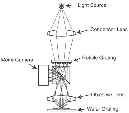
32 Introduction Reticle Grating Moiré Camera Wafer Grating Light Source Condenser Lens Objective Lens
Figure 1-3: Two accurate gratings enable in-situ measurement of the objective-lens distortion in a stepper via a moir´e technique. Schematic only.
interferometry for stage position measurement. If accurate large-dimension gratings can be made, they will permit the replacement of laser interferometers with grating-based interferometers of high accuracy. The idea of using gratings to measure displace-ment is not new. In 1967, Gerasimov impledisplace-mented a grating interferometer to control the position of the carriage on a ruling engine [37]. He employed a pair of gratings, one transmission and one reflection, and used an achromatic setup depicted schemat-ically in Figure 1-42. Reference [38] points out the many advantages of grating-based
interferometry. Besides the cost and weight savings, the small optical paths involved in a grating interferometer make the scheme essentially immune to environmental dis-turbances, which have plagued laser interferometry from the beginning. Patterning the grating onto a thermally stable substrate like Zerodur can substantially enhance the repeatability of the interferometer. Today, displacement measuring grating in-terferometers, also known as linear encoders, are commercially available and have a variety of interesting designs [39]. They offer very good resolution, but in terms of measurement accuracy, they are still far behind the top-of-the-line laser interferome-ters3. The lack of accuracy is largely due to the present lack of technology to pattern
nanometer-accurate gratings over large dimensions.
2Figure adopted from Reference [37] and modi¯ed for better illustration.
3For instance, the LIP 382 Exposed Linear Encoder by Heidenhain has a resolution speci¯cation
1.4 Scanning beam interference lithography 33
Lamp
Beamsplitter
Transmission Grating (moving with the carriage)
Reflection Grating (fixed on base of the engine) Mirror Lens
Detector
Figure 1-4: A displacement measuring grating interferometer used to control a ruling engine. The reflection grating has half the spatial frequency of the transmission grating. The reflection grating is used at§2-orders whereas the transmission grating at zero and first order. One fringe cycle observed at the detector corresponds to a relative displacement of one-quarter the period of the reflection grating.
1.4
Scanning beam interference lithography
By interfering two small diameter Gaussian laser beams [41] and step-and-scanning the resulting interference image, SBIL can pattern large-area linear gratings with nanometer overall phase accuracy. Given the insight from the previous section, SBIL is a technology that may enable paradigm shifts in both pattern placement metrology and displacement measuring interferometry [1, 42].
In this section, I introduce the SBIL concept, but first, I briefly describe the traditional interference lithography (IL) system at MIT.
1.4.1
Interference lithography at MIT
From elementary electromagnetism, one can easily deduce the period p of the inter-ference fringes at a substrate when two plane waves interfere,
p = λ
sin θ1+ sin θ2
, (1.5)
where λ is the wavelength, θ1 and θ2 are the incident angles for the left and the right
arm, respectively (Fig. 1-5). When θ1 = θ2 ´ θ, Eq. (1.5) reduces to
p = λ
2 sin θ . (1.6)
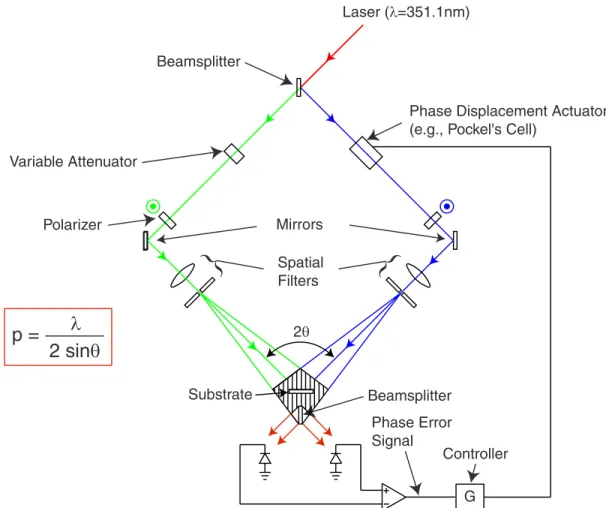
Reference [23] provides a good description of IL and its history. Figure 1-6 illus-trates the MIT system setup. As drawn, the two incident angles are assumed equal. The split beams from an argon-ion laser (λ = 351.1 nm) are conditioned before
in-34 Introduction Substrate ER EL q1 q2 Resist
Figure 1-5: During interference lithography, the nominal fringe period p at the sub-strate is determined by the beam incident angles θ1and θ2, and the laser’s wavelength
λ.
terfering at the substrate. The variable attenuator equalizes the power of the beams to maximize the fringe contrast. Polarizers in each arm ensure s-polarized4 light
ex-posing the substrate. Spatial filters rid wavefront distortions by blocking undesired spatial frequencies. The focal length of the lens in the spatial filter is chosen to set the divergence of the beams, thereby defining the size of the interference region. The beams have a Gaussian intensity distribution. For good dose uniformity, the spot size on the substrate should be much larger than the desired patterning area. A phase error sensor located near the plane of the substrate measures fringe drift, which is mainly due to air index change, vibration, and thermal drift of the optical setup. A differential signal from two photodiodes yields the error signal that drives the ana-log controller for a phase displacement actuator (a Pockel’s cell), which actuates to stabilize the fringes at the substrate.
The distance from the spatial-filter pinhole to the substrate defines the radius of the expanding spherical wavefront. It is desirable for this distance to be large for reduced hyperbolic grating phase nonlinearities [23, 43, 44, 45]. In practice however, turbulence, vibration, and thermal drift limit how large the propagation distance can be. In the MIT setup, this distance is nominally 1 m. Even with such large wavefront radii and the assumption of perfectly aligned beams, Figure 1-7 shows that the image diameter with subnanometer phase nonlinearity is only 2.8 mm. This assumes a 400 nm nominal grating period. Furthermore, if one considers a 20 mm£ 20 mm square area, the discrepancy worsens to over 600 nm at the four corners of the square5.
4Also known as the transverse-electric (TE) polarization.
1.4 Scanning beam interference lithography 35
Variable Attenuator
Phase Displacement Actuator (e.g., Pockel's Cell)
Spatial Filters Phase Error Signal Beamsplitter Substrate Mirrors Laser (l=351.1nm) 2q
{
{
G Controller Beamsplitter p = l 2 sinq PolarizerFigure 1-6: A schematic diagram of the traditional interference lithography system at MIT.
Theoretically, lenses may be used to collimate the beams after the spatial filter and thus eliminate the hyperbolic phase nonlinearity. However, it is questionable whether it is practical to fabricate, align and keep clean large optics capable of producing meter-sized gratings with nanometer phase nonlinearity.
For the purpose of conducting pattern placement metrology or displacement mea-suring interferometry, it is most ideal to have linear gratings, but the requirement is not absolute. If the nonlinear phase in the IL-produced gratings is highly repeatable and well characterized, one can still use them and compensate for the nonlinearity via a look-up table. However, Ferrera showed conclusively that nanometer repeatability for traditional IL is improbable if not impossible to attain because of severe beam and substrate alignment requirements [23]. For example, he showed that in order to attain a repeatability of 3 nm over an area of 25 mm£ 25 mm, the two interferometer arms dL and dR in Figure 1-7(a) must be matched to 150 nm. With much technical
36 Introduction
(a)
(b)
p
=
λ
2 sin
θ
x
z
y
q
q
d
Ld
RDiscrepancy from linear phase for dL = dR = 1 m
x (mm) y (mm) -2 -1 0 1 2 -2 -1 0 1 2 0 nm 1 nm -1 nm 3 nm 5 nm -3 nm -5 nm
Figure 1-7: Nonlinear phase distortions due to the interference of two spherical waves with 1 m wavefront radii, assuming that the system is in perfect alignment and is set up for a nominal grating period of 400 nm. (a) The interference coordinates. (b) Phase discrepancy from an ideal linear grating. The region with subnanometer nonlinear phase is less than 2.8 mm in diameter.
1.4 Scanning beam interference lithography 37
400 nm period gratings over an area of 30 mm£ 30 mm.
Because of phase nonlinearity and repeatability issues, conventional IL is incapable of producing large-area linear gratings.
1.4.2
SBIL concept
Figure 1-8 depicts the SBIL system concept. A grating beamsplitter splits the laser in two. The lithography interferometer optics closely resembles that of traditional IL but the grating image is much smaller than the total desired patterning area. The beams are Gaussian in nature. The 1/e2 intensity diameter at the substrate is
typically 2 mm, but can be enlarged or reduced by adjusting the optical layout. The collimating lenses after the spatial filters ensure that the Gaussian beams interfere with each other at their waists, where the wavefronts are the most planar6. For a
lithography laser wavelength of λ = 351.1 nm, the system is intended for writing gratings with a period in the range of 200 nm to 2 µm. The substrate is mounted on a laser interferometer controlled air-bearing XY stage. Large gratings are fabricated by scanning the substrate at a constant velocity underneath the grating image.
Figure 1-9 illustrates how SBIL achieves a uniform exposure dose by overlapping scans. Figure 1-9(a) shows the grating image being scanned along the substrate. In order to stitch scans together, one must measure the fringe period with high accuracy. SBIL period measurement goal is 1 nm uncertainty over 1 mm-radius spot, which translates into an allowed percentage measurement error of only one-part-per-million (1 ppm). At the end of the scan the stage steps over by an integer number of fringe periods and reverses direction for a new scan. SBIL has the significant added complexity over IL of accurately synchronizing the interference image to a moving substrate. The scanning grating image is illustrated in Figure 1-9(b). The interference pattern has a Gaussian intensity envelope. The effective number of fringes in the grating image may be many thousands (i.e., 5,000 fringes in a grating image with a 2 mm 1/e2-diameter and a 400 nm period). Figure 1-9(c) shows the individual scan
intensity envelopes in dashed lines and the sum of the envelopes in a solid line. A maximum step size is constrained by the desired dose uniformity. As plotted, a step size of 0.9 times the 1/e2-radius produces dose uniformity of better than 1%.
Similar to IL, SBIL employs a fringe-locking controller to stabilize the fringes while writing. Unlike IL’s homodyne approach, which stabilizes the fringes by sensing the differential intensity variations between two photodiodes, SBIL uses a heterodyne fringe-locking scheme. Since phase drifts are detected in the frequency domain, the
6Reference [45] shows that uncollimated Gaussian beams can also be used to generate a
proper-sized grating image. However, the topology is not currently used due to optics packaging reasons. See Section 5.2.11 for details.
38 Introduction Grating Beamsplitter UV Laser (l) Variable Attenuator Phase Error Signal 2q Mirror Spatial Filter Beam Pickoffs Beamsplitter Phase Displacement Actuator Controller G Stage Error S + + Substrate
Stage Interferometer Mirror Column Reference Mirror
Stage Displacement Measuring Interferometer Air Bearing XY Stage Grating Patch Polarizer Period: p = l 2 sinq x y z
Figure 1-8: Scanning beam interference lithography system concept.
X Direction Y Direction Scanning Grating Image Air-bearing XY Stage Resist-coated Substrate X Summed Intensity of Scans 1-6 X Grating Period, p Intensity, scanning grating image
Intensity, sum of overlapping scans
Individual Scan (only intensity envelope shown)
a)
b)
c)
Figure 1-9: SBIL step-and-scan scheme. (a) Top view. The step and scan directions are x and y, respectively, which are also defined in Figure 1-8. To ensure good stitching between adjacent scans, the stage must step over by an integer number of fringe periods. (b) Gaussian intensity envelope of one scan. Period exaggerated. (c) Beam overlapping to create a uniform exposure dose.
1.4 Scanning beam interference lithography 39
heterodyne scheme is immune to laser intensity fluctuations, which can be quite significant over an hour time required to pattern a 300 mm grating. It should be noted that besides fringe motions due to the changing air index, the nonideal motion of the stage, if uncorrected, introduces additional errors in the written grating as well. For that reason, stage positioning error, especially along the sensitive x axis which is perpendicular to the fringe direction, is also compensated by fringe locking.
1.4.3
System advantages
SBIL offers significant advantages over IL. The small beams used in SBIL provide a major benefit in ease of obtaining small wavefront distortions and thereby a highly lin-ear grating image within the interference spot [45]. Nowadays, commercial optics with figure errors, typically one-tenth of a wave (i.e., λ/10) across a one-inch (25.4 mm) clear aperture, is readily available at modest prices. Because SBIL employs small beams a couple of millimeters in diameter, they sample only a tiny fraction of the overall aperture. Therefore, the effective figure error is much smaller than λ/10.
By scanning the grating image, nonlinear distortions along the scan direction can be averaged out, so can phase jitters due to imperfect fringe locking and stage motion. Overlapping adjacent scans leads to further and more significant averaging of the phase nonlinearity; it also allows flexibility in controlling the resist grating period at the picometer level–both are subjects that I will examine in great detail in this thesis. Also, critical alignments such as lens positioning and angle of interference are much relaxed for small beams.
SBIL really is a fusion of IL and mechanical ruling. Taking the best from both worlds, our prototype tool is appropriately nicknamed “Nanoruler”. Instead of a single diamond tip, SBIL in a sense writes with thousands of “tips” in parallel, which dramatically improves the system throughout. For example, to create a grating 300 mm£ 300 mm in size with a period of 400 nm, the current state-of-the-art ruling engine, under a most ideal scenario, has to run continuously for 52 days, whereas Nanoruler can finish the job around an hour. By permitting adjustments of the stage scan speed, overlapping step size, and beam power, SBIL also allows good exposure dose control.
1.4.4
System overview
Figures 1-10 and 1-11 show the front and the back of the SBIL prototype, respectively. The system employs an XY air-bearing stage7, column referencing heterodyne
inter-ferometry, refractometry, a grating length-scale reference, beam steering system, beam alignment system, in-situ fringe period measurement, wavefront metrology,
40 Introduction
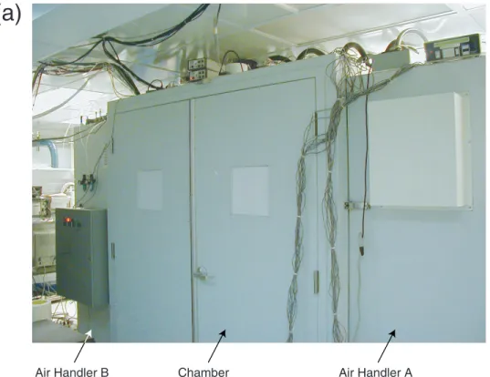
optic fringe locking, and active vibration isolation. Figure 1-12 shows a custom-built Class 10 environmental enclosure 8 that provides acoustic attenuation, particle and ambient-light protection, as well as controls over temperature (§0.005◦K), relative
humidity (<§0.8%), and pressure gradient (< 15.5 Pa/m). Displacement measuring interferometer
The most salient difference between traditional IL and SBIL is the step-and-scan feature provided by an XY air-bearing stage. The stage is controlled via displace-ment measuring interferometry (DMI)9. Large gratings are fabricated by scanning the
substrate at a constant velocity underneath a small grating image. By design, the interference fringes are oriented along the stage y axis, which I will also refer to as the scan direction. The stage x axis is perpendicular to the fringes, and it defines what-I-will-call the step direction.
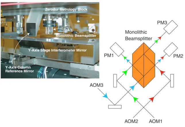
Presently, two two-pass column-referencing heterodyne interferometers, each with 0.31 nm resolution, measure the critical x-axis displacement and yaw (Fig. 1-17). The hardwares for doing column referencing along the y axis are in place but not yet im-plemented. Error terms [27, 28, 46], such as the electronics error, polarization mixing error and mirror alignment error, all impact the accuracy of the DMI measurements, thence stage performance. Their effects combine into the so-called stage error, which must be minimized during SBIL writing via real-time fringe locking. Furthermore, changes in the index of air and the vacuum wavelength of the DMI laser require an accurate way to scale the phase readings from the heterodyne electronics. A grating length-scale reference has been proposed [47], which will be incorporated on the vac-uum chuck to calibrate the wavelength of the stage interferometer (Fig. 1-17). The system is designed to read the phase of a grating that has nominally the same period as the one that it is set up to write [48]. Once calibrated, the system employs a refractometer, essentially a stationary interferometer, to continuously monitor the air index-change induced wavelength change, thus allows real-time correction of the inter-ferometer readout. To reject stage motion induced disturbances, an active vibration isolation system10 with feed-forward control is used.
Lithography interferometer
To reduce a major source of thermal and mechanical disturbance, and to allow multiple lithography tools to share a common laser, the UV lithography laser (λ = 351.1 nm) is located far (» 10 m) from the SBIL system. A beam steering system [49] is used to stabilize the position and angle of the beam as it reaches the SBIL tool
8Built by Control Solutions LLC, Inc.
9DMI hardwares are manufactured by Zygo Corporation.
1.4 Scanning beam interference lithography 41
Optical Bench with Interf
erence Lithog
raph
y
and Metrology Optics Gr
anite Base
Isolation System
X-Y Air Bear
ing
Stage
Metrology Bloc
k with
Phase Measurement Optics
Chuc k Wa fe r Receiving T o w e r
for UV Laser (λ = 351.1 nm) X-axis Interf
erometer
Refr
actometer
Figure 1-10: SBIL system, front view. Currently configured to write 400 nm period gratings. The whole system is housed inside a Class 10 environmental chamber.
42 Introduction
Laser Receiving To
w
e
r
HeNe Stage Interf
erometer Laser Stage Beam Steer ing System Ve rtical Optical
Bench Y-axis Interf
erometer
Laser (
l
= 351.1 nm)
1.4 Scanning beam interference lithography 43
Heat Ducts from the Acousto-Optic Modulators (AOMs)
Air Handler B Ultra-Low PenetrationAir (ULPA) Filters Air Handler A Air Handler A Chamber
Air Handler B
(a)
(b)
Figure 1-12: SBIL environmental enclosure. (a) External view. (b) Internal view with air flow paths outlined. All major thermal sources, which include the HeNe stage interferometer laser and all three acousto-optic modulators (AOMs), have been enclosed. Heat is actively pumped away from the optical bench via ducts.
44 Introduction
and forms the lithography interferometer.
The optical design and layout of the interferometer, which will be discussed in detail in Chapter 2, incorporates means for spatial filtering and adjustment of laser intensity, polarization, and wavefront curvature (Fig. 1-13). A§1-order grating beam-splitter is used to separate the incoming laser into two beams that form the two arms of the interferometer. The use of the grating provides a greater tolerance on the beam angular instability [49]. In turn, this leads to superior fringe period stabilization. Ap-pendix B discusses the physics. The grating also yields an achromatic configuration where the period of the interference fringes is insensitive to air index changes and vacuum wavelength variations of the UV laser [50, 51, 52].
Currently, the system is set up to write gratings with a nominal period of around 400 nm. While the system is capable of writing periods as small as 200 nm and as large as 2 µm, once the interference optics have been laid down for a particular period, switching to another period is impossible unless all the optics are relocated. The present goal of SBIL is to demonstrate writing with nanometer phase accuracy at a fixed period, e.g., 400 nm. Variable period writing is an interesting and practical research topic for the future.
During SBIL writing, lithography interferometer’s phase error and the stage error are fed back to a high bandwidth heterodyne acousto-optic fringe locking system, which in real-time, locks the interference fringes to the moving substrate [53]. Figure 1-14(a) shows a schematic of the system in the so-called writing or lithography mode. An acousto-optic modulator is a device that can both diffract and shift the frequency of the diffracted beam [54]. In the case of SBIL, all three AOMs are tuned to diffract strongly in the first order. By setting the frequencies with a master frequency syn-thesizer11and combining the diffracted beams appropriately, two 20 MHz heterodyne
signals at phase meters (PM) 1 and 2 are produced. A digital signal processor (DSP) then compares the signals and drives AOM2 to keep the phase difference between the two arms constant. The performance of the fringe locking system is limited by the controller’s bandwidth and inaccuracy in the fringe locking sensor signal due to air index variations and electronic inaccuracy. It is important to note that the stage error is also fed to the fringe locking system and compensated in real-time. SBIL tool’s re-peatability is established by reading the phase of a previously exposed grating. Figure 1-14(b) is a schematic of the so-called grating reading mode. A SBIL-written grat-ing is used in the Littrow condition, where the 0-order reflected beam from one arm coincides with the -1-order back-diffracted beam from the other arm. Two 20 MHz