The Development of Novel Passive and Active
Photonic-Crystal Devices
Solomon Assefa
B.S., Electrical Engineering and Computer Science
Massachusetts Institute of Technology (2001)
B.S., Physics
Massachusetts Institute of Technology (2001)
M.Eng., Electrical Engineering and Computer Science
Massachusetts Institute of Technology (2001)
Submitted to the
Department of Electrical Engineering and Computer Science
in partial fulfillment of the requirements for the degree ofDoctor of Philosophy in Electrical Engineering
at theMASSACHUSETTS INSTITUTE OF TECHNOLOGY June 2004
c 2004 Massachusetts Institute of Technology
All rights reserved.
Department
..
...
...
Solomon Assefa of Electrical Engineering and Computer Science
14 May 2004
Certified by.... ...
Leslie A. Kolodziejski P1rofessor of Electrical Engineering Thesis Supervisor
Accepted by... ...
Arthur C. Smith
Chair, Department Committee of Graduate Students
MASSA HUSETT SuT epartment of Electrical Engineering and Computer Science OF TECHNOLO'.g\/
Author..
The Development of Novel Passive and Active
Photonic-Crystal Devices
by
Solomon Assefa
Submitted to the Department of Electrical Engineering and Computer Science on 14 May 2004, in partial fulfillment of the
requirement of the degree of
Doctor of Philosophy in Electrical Engineering
Abstract
Photonic crystals are anticipated to have impact on large-scale photonic integrated-circuits by allowing the creation of compact and efficient devices such as waveguides, splitters, microcavity filters, light emitting diodes, and lasers. Previous experimental research has mainly focused on photonic crystals composed of a lattice of air holes etched into dielectric slabs. This thesis discusses the design, fabrication, and characterization of the "inverse" structure, a square lattice of dielectric-rods in air. Bandgap guiding of 1.5 gm light is experimentally demonstrated for a photonic-crystal waveguide created by introducing a line-defect of smaller-radii rods. To provide efficient optical coupling between input/output dielectric waveguides and the photonic-crystal waveguide, an adiabatic taper having two stages is employed.
Furthermore, the thesis investigates novel photonic -crystal devices and fabrication schemes. An expose-develop-etch (EDE) method is utilized to fabricate rod-based photonic-crystal devices in Ill-V and SOI material systems. The thesis also presents an electrically-activated linear-waveguide photonic -crystal laser. A compact microcavity is created by introducing a defect inside a one-dimensional photonic crystal. Electrical-activation and edge-emission are achieved by patterning microcavity waveguides into p-i-n-doped epitaxial heterostructures. The compact photonic-crystal laser is anticipated to have impact on the integration of optical devices on the same chip.
Thesis Supervisor: Leslie A. Kolodziejski Title: Professor of Electrical Engineering
Acknowledgement
I vividly remember the day I arrived at MIT, my first time in the US, as a young
freshman on August 18, 1996. During the last eight years, I have learned a lot and have
gotten the opportunity to explore the latest research efforts. MIT is a world-class institute
that has many brilliant people with innovative ideas. I definitely enjoyed the daily
intellectual challenge, and benefited from the people around me. I am very grateful to many people who contributed to my success during the amazing time I spent at MIT.
First, I would like to thank my advisor Professor Leslie Kolodziejski. I joined
Leslie's group as a curious undergraduate student; motivated by the novel research
conducted in her. lab, I continued my education as a graduate student. Leslie has consistently provided me with the full support and mentorship that I needed throughout
graduate school. She has taught me the value of unique research, and encouraged me to
discover and pursue the road that is less traveled. Indeed, Leslie is an exemplary
educator and mentor.
I would like to thank Dr. Gale Petrich for his support and friendship. Gale has
helped me become a seasoned graduate student by encouraging me to perform thorough
research. He devoted his time to discuss my research and edit my papers. Collaborating
with a scientist as wise, helpful, and kind as Gale was incredibly useful.
I would like to thank Professor Henry Smith for encouraging and mentoring me
impressed by his interest in various cultures and his knowledge of history. Moreover, I
would also like to thank Professor Erich Ippen and John Joannopoulos for their
constructive feedback and exchange of ideas. Their deep insight into the physics of
photonic crystals, and photonics in general, was very helpful.
I would also like to thank my collaborators Dr. Peter Bienstman and Dr. Steven
Johnson for the time they spent simulating the devices. My deep appreciation goes to
Peter Rakich, who devoted a lot of time with me to optically characterize the devices.
Peter's interest in the drum beats of North African music helped us work long hours in
the lab. I would also like to thank Jim Daley for kindly facilitating my research in NSL
and for being very accommodating. My special appreciation goes to Mark Mondol for
the numerous hours he spent performing e-beam lithography. Our intense discussion
about US politics and international affairs was very enlightening.
I enjoyed working with all members of Leslie's research group. I thank my
former officemate Alexei Erchak, who helped me start my research in the "Microlab".
Alexei and I brewed strong coffee every morning in our office - besides saving us money, the ritual led to productive 14-hr work days! I appreciate the friendship of
Aleksandra Markina, with whom I took many physics classes as an undergraduate
student; the creatively decorated Easter eggs that Aleksandra gave me every year
reminded me to celebrate and enjoy the Orthodox Christian Easter holiday. I would like
to thank Sheila Tandon and Ryan Williams for the good time I have spent with them
inside and outside of the lab; the 'water cooler' in their office provided me with a great
opportunity to discuss research, MIT, life, etc. I appreciate Reginald's sincere friendship,
apartment; I also had fun working on the fabrication of the nano-switch. Moreover, I
wish success to Sarah Rodriguez, Yamini Kangude, and Eric Mattson. They were
awesome officemates and I enjoyed showing them how 'things' work in the lab.
I would also like to thank all of my friends: Yohannes Tsehai, Befekadu Ayenew,
Efrem Tekle, Paul Njoroge, Martin Mbaya, Saria Hassan, and many others who have
been a healthy distraction from long days in the lab. I am grateful to my host parents
Kate and Gordon Baty, wxho helped me adjust to life in the US and encouraged me to pursue my PhD at MIT. I would like to thank my friends in the MIT-Africa Internet
Technology Initiative (MIT-AITI), a program established at MIT by Paul, Martin, and I.
MIT-AITI was my passion whenever I had a break from my research. My heartfelt love
and deep gratitude goes to my closest friend Becky, who listened to all of my stories with patience, always made me smile and have faith, and encouraged me everyday while I was
writing the thesis.
I don't even have the words to express my gratitude towards my family. I would
like to thank my Mom and Dad for their dedication, and for teaching me honesty, love,
and hard work. My special appreciation goes to my eldest brother Bekure, who is my
inspiration, confidant, mentor, and role model. My love goes to my dear sisters
Woinishet and Meaza for their care and concern about my happiness. Also, my deep
gratitude goes to my brothers Daniel and Teshome for encouraging me to aim high and
work hard for my goals. Finally, this PhD would not have been possible without my
dearest sister Hirut, whose love and care for her 'little brother Sol' motivated me to
Table of Contents
A B ST R A C T ...
2
ACKNOWLEDGEMENT...3
TABLE OF CONTENTS ... .6
LIST OF FIGURES ...
8
CHAPTER 1: Photonic Crystals: Background...15
1.1 M otivation... 15
1.2 Photonic Crystals: Introduction...18
1.3 The Physics of Photonic Crystals...21
1.4 The Development of Photonic Crystals...28
CHAPTER 2: Square Lattice of Dielectric Rods: Design...38
2.1 Overview: Why Use Dielectric Rods?... ... .... ... ... . . 38
2.2 Bandgap Engineering...39
2.3 Waveguide Engineering...44
2.4 Efficient Waveguide Coupling...48
CHAPTER 3: Square Lattice of Dielectric Rods: Fabrication...59
3.1 O verview ... 59
3.2 Epitaxial Material Growth...62
3.3 Scanning Electron Beam Lithography (SEBL)...65
3.4 Liftoff Process...74
3.5 Reactive Ion Etching...76
3.6 C leaving...90
3.7 W et O xidation...91
CHAPTER 4: Square Lattice of Dielectric Rods: Devices...99
4.1 O verview ... 99
4.2 Photonic Crystals: Generation-I through Generation-V...100
4.3 Photonic Crystal Waveguides: Introducing Defects...109
CHAPTER 5: Square Lattice of Dielectric Rods: Optical
Characterization...114
5.1 Characterization Setup...114
5.2 D evices on Sam ple...116
5.3 Dielectric Waveguide Characterization Result...117
5.4 Bandgap Characterization Result...120
5.5 Photonic-Crystal Waveguide Coupling Characterization...121
5.6 Coupling and Guiding Efficiency...122
5.7 Optical Characterization Conclusion...125
CHAPTER 6: Passive and Active Photonic Crystals: Novel Devices and Fabrication Techniques...127
6.1 O verview ... 127
6.2 HSQ for Fabrication of Photonic-Crystal Devices...128
6.3 Electrically-Activated Linear-Waveguide Photonic-Crystal Microcavity L aser...139
CHAPTER 7: Conclusion and Future...153
7.1 A ccom plishm ents...153
7.2 Future Work...155
List of Figures
Fig. 1-1: Schematic illustration of photonic crystals a) one-dimensional (ID) b) two-dimensional (2D)
c) three-dimensional (3D). In each figure, the index contrast is indicated by the difference in co lor... . . 1 8
Fig. 1-2: Schematic illustration of 2D slab photonic crystals. a) Square lattice of pillars. Each pillar has a high-index guiding layer surrounded by low index top and bottom layer. b) Triangular lattice of air holes etched into a high index dielectric slab...20
Fig. 1-3: Schematic illustration of band diagrams for a dielectric stack wherein a) Ej=1 and E2=1 b)
E-1=12 and E2=13 c) 81=1 and E2=13...25
Fig. 1-4: SEM images of a) woodpile structure made by layer by layer processing b) structure in a after
tungsten deposition and silicon removal c) wood-pile structure made by wafer-fusion d) individual layers that will be stacked on each other by micromanipulation ... 29
Fig. 1-5: SEM images of a) opal colloidal photonic crystal composed of silica spheres b) inverse-opal structure after silicon infiltration and removal of the silica spheres...30 Fig. 1-6: SEM images of 3D photonic crystals a) created in resist by two-photon absorption b) patterned
in resist by holographic lithography c) the inverse of the structure in (b) after metal evaporation and rem oval of the resist tem plate... 31
Fig. 1-7: SEM images of slab photonic crystals waveguides created by a) removing one row of holes b) rem oving three row s of holes... 33
Fig. 1-8: SEM of slab photonic crystal waveguides bends a) 600 b) 900 c) 120...34 Fig. 1-9: Schematic of coupling from embedded active region into the photonic crystal...36 Fig. 1-10: Schematic of a) the mode of the ridge waveguide b) the mode coupling into the tapered
photonic crystal w aveguide... 36
Fig. 1-11: Schematic of a) coupling from a ridge waveguide into a photonic crystal waveguide by introducing holes progressively b) using the same procedure to couple two photonic crystals of
different w idth ... 37
Fig. 2-1: Various configurations of a photonic crystal consisting of rods a) the low index substrate below and above the rods create symmetry b) low index cap and stilt surrounding the rods create symmetry c) asymmetric structure with low index stilt...41 Fig. 2-2: a) Schematic of the simulated structure consisting of 0.83pm GaAs guiding layer, 0.6pm AlxOY
stilts, 0.9pm AlxOY spacer layer, and GaAs substrate. b) The simulated band structure indicates a
bandgap from 0.29 to 0.32 (c/a). c) The simulation of transmission through the structures a bandgap for TM w hile there is no gap for TE...43
Fig. 2-3: a) Schematic of the simulated structure consisting of 0.83pm GaAs guiding layer, 0.6pm AlOy
stilts, 0.9 pm AlXOy spacer layer, and GaAs substrate. While the photonic crystal rods have diameter of 300nm, the defect rods have diameter of 250nm. b) Scanning electron micrograph (SEM) image of the pattern after the electron beam lithography (e-beam) step shows the defects inside the photonic
crystal... .... 46
Fig. 2-4: a) The projected band structure shows that as the radius of the defect rods is decreased, the defect band moves up in the bandgap. Simulation shows the mode profile is well localized in the defect rods
b) a horizontal cut through the photonic crystal c) a vertical cut through the photonic
crystal... ....47
Fig. 2-5: a) SEM image of the butt-coupling approach patterned in PMMA. b) Power transmission sim ulation result of the structure in (a)...49 Fig. 2-6: a) SEM image of the tapered waveguide coupling patterned in PMMA. b) Power transmission
sim ulation result of the structure in (a)...51 Fig. 2-7: a) SEM image of the tapered waveguide inserted into the photonic crystal showing the coupling
input region and the photonic crystal region. The arrows indicate that the dielectric waveguide has a mode with completely forward propagating field component, while the photonic-crystal waveguide has both forward and backward propagating field components. Also, the guiding is high-index guiding in the 'coupling input' region, while the guiding in the photonic-crystal 'guiding region' is low-index guiding due to the reduced radius of the rods. b) The new coupling approach solves the problems in
(a) by dividing the 'coupling input' into two adiabatically tapered stages...52 Fig. 2-8: a) Simulated mode profile through the first coupling stage. b) Simulated power transmission
through the first stage... .. .... 54
Fig. 2-9: a) The schematic shows slowly insertion of the photonic-crystal rods. b) The simulated power
transmission through the structure shows inefficient coupling [127]...56
Fig. 2-10: a) Simulated mode profile through the new adiabatic coupling approach. b) Simulated
transmission through the structure shows efficient and high transmission that is only weakly dependent on the length of the photonic crystal waveguide...57 Fig. 2-11: Power transmission result (3D simulation) comparing three different coupling approaches. The
defect rod radius of Taper 1 is 0.25a while that of Taper 2 is 0.23a...58 Fig 3-1: Schematics of a) a wafer cleaved into many pieces after epitaxial growth b) each piece, which
has many sets of devices, is cleaved at the vertical lines at the end of processing c) each set has many photonic crystals, and the cleave propagates through each of the input/output dielectric w aveguides... . ... 60
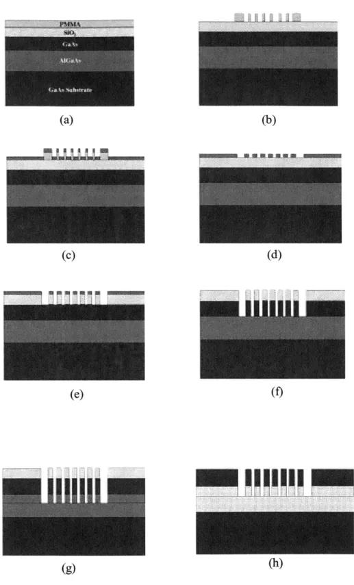
Fig 3-2: Schematics of the process sequence involved in making the photonic crystals: a) Si02 sputter-deposition and PMMA spinning b) e-beam exposure and development c) nickel evaporation d) nickel liftoff e) Si0 2 etch f) nickel wet etch and GaAs etch g) AlGaAs etch h) Si02 etch and AlGaAs
oxidation into AlxOy...61
Fig 3-3: SEM of epitaxially grown heterostructure. The structure consists of 0.86pm GaAs layer and 1.5pm AlO.9GaO.IAs layer on a GaAs substrate...64 Fig 3-4: Schematic representation of the integrated MBE system...64
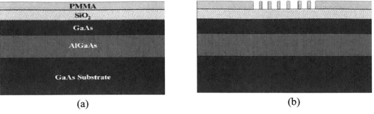
Fig. 3-6: Schematic illustration of a) sample after spinning PMMA b) after e-beam exposure and
developm ent...69
Fig. 3-7: a) Schematic illustration of a square divided into pixels. The beam diameter is bigger than each pixel. b) The superposition of the exposure of pixels results in a circular feature at a higher dose. c)
SEM of circular hole patterns, which are initially designed as squares (inset) in a CAD
file ... . . .. 70 Fig. 3-8: a) Schematic illustration of a waveguide divided into pixels. The beam diameter is larger than the pixel. b) The superposition of the exposed single pixels results in a waveguide that is wider than the d esig n ... 7 0 Fig. 3-9: a) SEM image of a photonic crystal without adjacent straight waveguides. b) Schematic
illustration of a straight waveguide next to the photonic crystal. c) SEM image demonstrating the effect of having wide waveguides designed adjacent to the photonic crystal...71 Fig. 3-10: a) Schematic illustration of a straight waveguide adjacent to the photonic crystal. b) The SEM
demonstrates that the proximity effect can be adjusted by using the correct dose and separation between the waveguide and the photonic crystal...71 Fig. 3-11: Schematic illustrations of stitching errors. a) The scan field length is shorter than stage field
length (field scaling error). b) The scan field length larger than the stage field length (scaling error). c) The deflection axis is misaligned with the stage axis (field rotation error). d) The correct
calibration gives well aligned waveguides...72 Fig. 3-12: SEM image illustrating the stitching of 500nm wide waveguides at the interface of 256pm fields.
The field interface is indicated by the dashed vertical line. Good calibration results in 25nm stitching erro r...7 4 Fig 3-13: SEM images of PBG patterns after liftoff. a) The ultrasonic agitation partially strips of the photonic crystal and the adjacent waveguides. b) Leaving the sample in NMP solution for longer period results in a good liftoff...75
Fig. 3-14: Grating patterns on a film. a) Pattern before etch. b) Pattern has isotropic sidewalls after wet etch. c) Pattern has anisotropic sidewall after a dry etch...76
Fig. 3-15: Schematic representation of a dry etching process [139]...78
Fig. 3-16: a) Schematic representation of an RIE. b) The energy distribution of electrons...79
Fig.3-17: a) SEM of a partially etched Si02 waveguide used for etch-rate calibration. b) Etch rate for the sputter-deposited Si0 2... . . . .. 81
Fig. 3-18: SEM of periodic oxide pillars after the Ni has been wet etched...82
Fig. 3-19: SEM of GaAs/AlGaAs etched in BCl3 plasma at a) high pressure b) low pressure...84 Fig 3-20: a) Ion and radical effect on the film and the mask during ion-enhanced anisotropic etching. b)
Enhancing anisotropy by intentionally forming a sidewall inhibitor...85 Fig. 3-21: a) A well calibrated anisotropic etch in BCl3 plasma. b) Etch rate of GaAs/AlGaAs in BCl
Fig. 3-22: a) Schematic illustration of staggered stair design. Arrows indicate where sample was cleaved
b) SEM image of the structure after etching in BCl3 plasma...88 Fig. 3-23: The SEM images show the etched waveguide almost flush with the cleaved facet...89 Fig. 3-24: The schematic representation shows the cleaved sample mounted to enable AFM detection of the
etched w aveguides... 89
Fig. 3-25: SEM images of cleaved waveguides. a) Cleaving the sample after oxidation results in a broken waveguide. b) Cleaving the sample before oxidation results in a smooth facet...90 Fig. 3-26: Schematic illustration of two limiting cases in AlxGa1xAs oxidation process a)
Reaction-limited. b) Diffusion-limited. CG, Cs, C , and Q are reactant concentration in steam, inside the oxide/steam interface, outside the oxide/steam interface, and at oxide/ AlxGaixAs interface...94
Fig. 3-27: Steam oxidation furnace setup [160]...96
Fig. 3-28: SEM image of grating structures after partial oxidation. The resist has not been totally removed from the oxide mask. The GaAs layer is 850nm thick and the Alo.9Gao.1 As is 1500nm thick...97 Fig. 3-29: a) The SEM image of a 1.5pm wide waveguide shows partial lateral and vertical oxidation. b)
SEM image of a 0.45pm waveguide shows complete lateral oxidation and partial vertical oxidation.
Both waveguides were oxidized for 11 minutes at 4150C...98
Fig. 3-30: Lateral and vertical oxidation rate characterization...98 Fig. 4-1: Process flow for Generation I devices...100 Fig. 4-2: SEM images of Generation-I devices. a) After e-beam exposure and development of PMMA. b)
After nickel evaporation and liftoff. c) After RIE of oxide and wet etch of nickel. d) After etching
into the G aA s layer...101
Fig. 4-3: Process flow for Generation II devices... . . ... 102
Fig. 4-4: SEM image of Generation-II devices. a) After the BCl3 RIE, the nickel mask is sputtered away.
b) The titanium mask does not withstand the etch conditions...103
Fig. 4-5: Process flow for Generation-III devices...103 Fig. 4-6: SEM images of Generation-III devices. a) Photonic crystal patterns in sputter-deposited Si0 2. b)
Patterns etched into GaAs/AlGaAs and oxidized. c) Close-up of (b). d) A set including two photonic crystal devices and a straight dielectric waveguide...104 Fig. 4-7: SEM images of Generation-IV devices. In (a) and (b), the oxide mask was completely sputtered
away. In (c) and (d), the oxide mask was partially sputtered away...105 Fig. 4-8: SEM of Generation-IV devices after etching improvement a) straight sidewall profile b) size of
rods is reduced by adjusting at the e-beam exposure step...106 Fig. 4-9: Final optim ized process flow ... 107
Fig. 4-10: The SEM images show photonic crystals that have been successfully fabricated and optically characterized. The number of columns was varied in order to observe the development of the bandgap as the coherent scattering increases. SEMs (a), (b), and (c) show the patterns after e-beam exposure and development in PMMA. SEMs (d) and (e) show a top-down view of the patterns at the end of the process while (f), (g), and (h) show side-view of the structures. The height of the GaAs layer is 500nm and the A lh O y is 1.2pm ... 108
Fig. 4-11: SEM image of the photonic-crystal waveguide in PMMA after e-beam exposure and development. The diameter of the defect hole is 245nm while that of the diameter of the photonic crystal is 297nm ... 110
Fig. 4-12: SEM of photonic crystal waveguides after e-beam exposure and development in PMMA. The number of columns is varied from 2 to 8 in order to investigate the loss incurred as a function of length. The input and output waveguides are 230nm wide. The diameter of the defects is 245nm while that of the photonic crystal is 290nm ... 110
Fig. 4-13: SEM images of coupling structures. a, b) The structure patterned in SiO2. c) The structure etched into GaAs/AlGaAs. d) A set of devices wherein the length (number of columns) of the
photonic crystal w aveguide is varied...111 Fig. 4-14: SEM of photonic crystal waveguides with tapered input and output coupling waveguides a)
after PMMA e-beam exposure and development b) at the end of the fabrication process with BCl3
etch and oxidation ... 112
Fig. 4-15: SEM of a novel coupling scheme for photonic crystal waveguides. a) and b) show the design after e-beam exposure and development in PMMA c) shows the coupled cavity waveguide without the cladding photonic crystal d) shows the complete photonic crystal waveguide with the coupling
structure e) and f) show a close up of the coupling scheme g) shows a top-down view of the etched structure h) shows a dielectric waveguide, coupled cavity structure, and coupling structure fabricated together on the sam e chip...113 Fig. 5-1: Optical characterization setup [162]...115 Fig. 5-2: a) IR image of the output facet of an array of waveguides. Light can be observed at the output
facet of one of the waveguides. b) The output is spatially filtered to filter out background radiation
m od es...1 15 Fig. 5-3: a) A set of devices consisting of a dielectric waveguide, and photonic crystal (no defect) of varying length. b) A set of devices consisting of a dielectric waveguide, coupled cavity waveguide, and a photonic crystal waveguide with adiabatic coupling scheme...116 Fig. 5-4: IR image of a) scattering loss as light is coupled from an input lens assembly into the input facet
of the dielectric waveguide, b) a broken waveguide leaking out the coupled light c) coupled light
being guided by a good quality dielectric waveguide...117 Fig. 5-5: TM and TE polarized light transmission power detected at the output facet of a straight dielectric
w avegu ide...119
Fig. 5-6: Comparison of transmitted power through two waveguides, one that has been oxidized for 8 m inutes and the other for 22 m inutes...119 Fig. 5-7: The top SEM images show photonic crystals with two and four rows. The graph plots the
measured normalized transmission through the structures. The photonic crystal with two rows does not have a bandgap. However, the photonic crystal with four rows demonstrates a bandgap for the
Fig. 5-8: Top down SEM image of a photonic-crystal waveguide with two-stage adiabatically tapered
coupling schem e...121
Fig. 5-9: Transmission through the device shown in Fig. 5-9 shows enhanced transmission inside the bandgap. The characterization of two similar devices on the same chip demonstrated similar and consistent pow er transm ission...122
Fig. 5-10: a) The four arrows indicate the wavelengths of light launched into the photonic crystal. b) IR image of the transmission through the photonic crystal. At 1454nm and 1460nm, which are wavelengths that have high transmission in (a), a bright streak is observed across the photonic crystal.
At 1445nm and 1470nm, which are at the band-edges, the streak disappears. In all of the images, the bright light indicates radiation loss. c) By comparing the radiation to an exact image of the photonic crystal (IR image taken under angular white light illumination), the radiation source is tracked to be the area of transition from the dielectric waveguide to the coupled cavity waveguides (roughly 10 Pm aw ay from the photonic crystal)...124 Fig. 5-11: a) SEM showing the coupled cavity waveguide without the cladding layer b) R image of the
transmission through the CCW in (a) shows large radiation at the transition region...125 Fig. 6-1: The cage structure of hydrogen silsesquioxane (HSQ) [168]...129 Fig. 6-2: The left side is the previous process sequence explained in Chapter 3. The shaded area of the
process sequence is replaced by the three-step HSQ process indicated on the right side...130 Fig. 6-3: SEM images of photonic crystal structures in HSQ on Si substrate after e-beam exposure and
development a) under-developed b) overexposed c) optimized exposure...131 Fig. 6-4: SEM image of photonic-crystal structures in HSQ on GaAs substrate after e-beam exposure and
development. a) The input waveguides were delaminated due to lack of adhesion. b) The photonic-crystal patterns w ere also delam inated...132 Fig. 6-5: SEM of photonic crystal structures in HSQ on GaAs substrate (with l0nm Si02 adhesion layer)
after e-beam exposure and development a-c) Photonic crystal without defects where the number of rows is varied. d-f) Photonic crystal with defect rows. g) A dielectric waveguide passing through a photonic crystal. h, i) Tapered input coupling. j) Waveguide bend. k) Add-drop filter design (based on S. Fan's design in R ef. 173)...133 Fig. 6-6: SEM images of GaAs/AlGaAs structures etched using HSQ mask. a) Before the removal of the
HSQ. b-d) Photonic crystals of varying number of rows after etching the HSQ mask. e) Adiabatically
tapered two-stage coupling structure after the HSQ mask is removed...135 Fig. 6-7: SEM images of photonic-crystal devices in SOI material system. a-c) Line-defect
photonic-crystal waveguides. d, e) Adiabatically tapered two-stage coupling structure. f, g) 900 bends. h)
Channel add-drop filter. i) Dielectric waveguide passing through the photonic crystal (designed based
on R ef. 118 and 175)...138 Fig. 6-8: a) The SEM image shows the photonic-crystal defect microcavity is created by eliminating one
hole and increasing the radius of two nearby holes. The laser, pumped with 830nm wavelength, shows external threshold pump power of 6.75mW [192]. b) The SEM image of a slab photonic-crystal fused to a low index substrate. The laser showed threshold pump power of 9.2mW for incident 980nm light
Fig. 6-10: a) Schematic of a ridge waveguide laser integrated with 2D photonic crystal next to the ridge
facet [197]. b) A ridge waveguide laser integrated with ID photonic crystal (DBR). One side has 5 mirror pairs while the emission side has 3 pairs...142 Fig. 6-11: Schematic showing a design for electrically-activated photonic crystal laser. Light is emitted
from the top waveguide in (a) while it is emitted from the bottom waveguide in (b)...143 Fig. 6-12: Schematic of the fabrication sequence: a) e-beam lithography b) top waveguide etch followed
by mask removal c) e-beam lithography of photonic crystal d) etch holes into the first layer, and then
etch deeper into the send layer to define the waveguide and the holes e) remove HSQ mask f)
photolithography to define undercut region g) final structure after undercutting, oxidation, and metal evaporation on contact pads...148 Fig. 6-13: Schematic of the epitaxially grown material system...149 Fig. 6-14: Room temperature photoluminescence experiment shows emission from the Ino 15Ga4.85As
quantum dots at -1280nm ... 150
Fig. 6-15: Optical micrographs of the contact pad and waveguide etched into the first layer...150 Fig. 6-16: a) The top-down SEM image shows the second layer was shifted from the first layer. b)
Side-view SEM image of the sample cleaved near a field boundary also Ahows field rotation error. Also, leftover HSQ is observed on the etched waveguide of the first layer...151 Fig. 6-17: a) SEM image of the HSQ after the e-beam exposure of the second layer shows the middle
waveguide and the second contact pad. Zooming into the middle section demonstrates the second layer is extremely well aligned on the etched first layer waveguide as seen in the SEM images in (c) an d (d )...15 2 Fig. 7-1: The SEM images illustrate 90'-bend waveguides with various coupling approaches. (a), (c), (e),
and (g) show bends with sharp corners. (b), (d), (f), and (h) show bends with resonators at the
Chapter 1
Photonic Crystals:
Background
1.1
Motivation
The last few decades have witnessed the transformation of telecommunication
networks [1]. The development of high speed transistors, semiconductor lasers and
detectors, and the enormous bandwidth provided by the large amount of fiber already
installed (but yet to be fully utilized) have resulted in the increase of information
transmission capacity. There is tremendous network traffic growth due to the current demand for high-speed data, and multimedia such as high-quality video [2].
However, the electronic circuits at network nodes which interconnect fibers only
meet the current communication bandwidth demand and will soon become a limitation
[3]. In the nodes, light is converted into electrons so that the electronic signal can be
re-shaped, re-timed, and re-amplified (3R regeneration), routed, buffered, etc.; then, the
electronic signal is converted back into light. This 'electronic bottleneck' at the nodes
leaves the large bandwidth of the fiber underutilized. Furthermore, the numerous racks
The network capacity can be increased, while lowering the cost, by packing functionality and intelligence into an optical-chip. Such chips, packed with optical
devices, will be able to identify the contents of the individual wavelengths of light in a
fiber, where each carries a specific video or voice data-stream. The chips will then route
each wavelength to a particular location after performing packet error correction and
3R-regeneration. If realized, the integrated optical-chip will replace racks of electronics for a
fraction of the cost [4].
A functionality required by the high-density photonic integrated-circuits is
guiding light around a bend with a radius of curvature on the order of a wavelength [5, 6].
To make this possible, high-index-contrast waveguides need to be utilized to guide light
on photonic chips. 'Ihough the radius of curvature to turn a corner is on the order of
microns, thus allowing high-density integration in a small area, the waveguides are very
susceptible to loss mechanisms such as scattering loss due to sidewall roughness
introduced during fabrication [7-11].
Photonic crystals have been proposed as a potential solution to guide light around
corners including 900 bends with near perfect transmission [12]. This will help reduce
the large area in current photonic chips due to the large radius of curvature of
waveguides, hence enhancing microphotonics device integration for high density
optoelectronic circuits. However, the practical use of photonic-crystal waveguides is
limited by the poor coupling efficiency between the photonic-crystal waveguide and
conventional index-guided waveguides. The photonic crystal waveguide to conventional
significantly different mode profile and propagation mechanism compared to traditional
waveguides that use index confinement.
Furthermore, optical 3R regeneration and optical logic functionalities capable of
performing header recognition and error correction have been demonstrated by
combining various discrete optical components, by using delay lines, external laser
sources, and lens assemblies that extend over many optical tables [13-17]. However,
such assemblies are too bulky and too costly to deploy at network nodes. Optical integration would be more efficient, practical, and economically advantageous if compact
enough to fit on an optical-chip. To this end, the implementation of all-optical 3R
regeneration and logic will require laser sources that interact with the incident light
carrying the information. Hence, photonic crystals can be utilized to create a compact
and efficient optical source for photonic integration.
This thesis focuses on how photonic crystals can be used to enhance the
performance of both active and passive devices, and allow the integration of photonic
devices on a chip. The major section of the thesis demonstrates photonic-crystal
waveguides created from a periodic arrangement of dielectric rods. The structures are
used for optoelectronic integration by solving the problem of coupling from high-index
conventional waveguides into low-index photonic crystal waveguides. The photonic
crystals have been fabricated in both III-V and SOI structures. Furthermore, a key
component that has been lacking from photonic crystals is their electrical activation. In
the last section of the thesis, a novel electrically-activated photonic-crystal
1.2
Photonic Crystals: Introduction
Photonic crystals are composed of materials with their dielectric constant
modulated in a periodic fashion. The periodic arrangement of high and low
refractive-index materials gives rise to a stop-band in which a range of frequencies are prevented
from propagating. Given the appropriate dimensions, the stop-band acts as a photonic
bandgap in which photons are prevented from propagating [18]. This is analogous to the
energy bandgap for electrons that is observed in electronic materials due to coherent Bragg scattering from the periodic variation in the electronic potential due to the
electronic structure of the atoms [19]. Lord Rayleigh performed the first study on
electromagnetic wave propagation in a material with one-dimensional periodicity in
1887, and Felix Bloch studied wave propagation in three-dimensionally-periodic media
in 1928 [20]. The existence of a complete bandgap for electromagnetic waves in a
photonic crystal was reported independently by Yablonovich [21] and John [22] in 1987.
a)
b) C)Fig. 1-1: Schematic illustration of photonic crystals a) one-dimensional (ID) b)
two-dimensional (2D) c) three-two-dimensional (3D). In each figure, the index contrast is indicated
Photonic crystals can be classified as one-dimensional (1D), two-dimensional
(2D), or three-dimensional (3D) [Fig. 1-1]. 3D photonic crystals are ideal because of
their complete bandgap [23]. However, they are difficult to fabricate at small length
scale due to the planar nature of the current semiconductor fabrication technology [24].
The best alternative to 3D photonic crystals is to emulate them with 2D photonic crystals combined with index confinement in the direction perpendicular to the plane of
periodicity [25]. These structures, in which a photonic crystal resides in the high-index material surrounded by low-index material, are known as slab photonic crystals. In the
plane of the photonic crystal, the confinement is due to the presence of a bandgap, while
the confinement in the vertical direction occurs due to the existence of a high-index
guiding layer surrounded by low-index cladding. The existence of the low index
surrounding gives rise to a light-cone, a region in the dispersion diagram that contains the
radiation modes guided by the background material. Even though these radiation modes
exist in the bandgap, a mode is still guided as long as the guiding layer has a higher
refractive-index with respect to the cladding layer.
Photonic crystals can be constructed in two main configurations as shown in Fig.
1-2. The first type consists of a periodic arrangement of high index dielectric material
(pillars) in a low index surrounding, which gives rise to a bandgap for the TM-like (odd)
mode where the E-field is polarized perpendicular to the plane of periodicity. The second
type consists of a periodic arrangement of lower index dielectric material (holes) in a
higher index slab, which gives rise to a bandgap for TE-like (even) modes where the
fabrication and testing. Other configurations that have been studied by many include
opals, inverse-opals, and self-assembled colloidal structures [26-28].
(a) (b)
Fig. 1-2: Schematic illustration of 2D slab photonic crystals. a) Square lattice of pillars. Each pillar has a high-index guiding layer surrounded by low index top and bottom layer. b)
Triangular lattice of air holes etched into a high index dielectric slab.
Photonic crystals have useful applications in compact optical devices such as
microcavities and waveguides. A photonic crystal microcavity is created by introducing
a defect in the periodic array and localizing a mode inside the bandgap. Furthermore, a
photonic crystal xxaveguide, which is created by introducing a row of defects, is useful
for routing light within a photonic integrated circuit. While the periodic arrangement of
dielectric material results in a photonic bandgap, the defect row functions as a waveguide
by localizing a band of frequencies. As a result, these frequencies propagate within the
defect row and are evanescent in the bulk photonic crystal. Perfect transmission through
900 bends have been calculated in 2D simulations of photonic-crystal waveguides that are
1.3
The Physics of Photonic Crystals
1.3.1 Maxwell's Equations
The propagation of waves in dielectric media is governed by Maxwell's
equations. Photonic crystals are created using materials which can be modeled as
isotropic and low loss, wherein the dielectric constant is approximated as having a
negligible imaginary component [18]. Using these facts, Maxwell's equations can be
summarized as follows:
V
*B(F,
t) = 0 (EQ-1.1) V XE(F,
t)= -B(F,
t) (EQ-1.2)a3t
V
0 D(,t)
= 0
(EQ-1.3)VXH(r,t)=
D(r,t)
(EQ-1.4)at
The time dependence in the equations can be eliminated by using time-harmonic fields.
Time-harmonic fields are useful because they cover the whole spectrum of the
electromagnetic waves, and Fourier analysis can be used to understand the time-domain
phenomena. Furthermore, any solution can be built by combining the time-harmonic
solutions through Fourier analysis [30]. By eliminating the time dependence, EQ-1.2 and
EQ-1.4 can be re-written as follows:
By decoupling the two equations, the final equation is expressed in terms of H as follows:
1
-Vx(
x (F))=
2H (F)
(EQ-1.7)e(r)
EQ-1.7 is the master equation for photonic crystals [18]. After solving for the magnetic
field at a given frequency, EQ-1.5 can be used to obtain the electric field.
1.3.2 Bloch States in Photonic Crystals
Analogous to quantum mechanics, electromagnetism in photonic crystals can be
stated as an eigenvalue problem in the frequency-domain approach by using H as the
eigenfunction and 0)2 as the eigenvalue. In quantum mechanics, a Hermitian operator 0
acting on two field vectors A and B has the property that (A, Q B) = ( Q A, B), where (A,
B) is the inner product of normalized vector fields A and B. A Hermitian operator
implies that the eigenfunctions are orthogonal and they have real eigenvalues. EQ-1.7
can be simplified by defining an electromagnetic operator as follows:
H
= V x(
x) (EQ-1.8)8(r)
This operator can be easily proven to be a Hermitian [18]. Because H is an eigenfunction
of H, it can be expressed as a linear combination of eigenmodes. For two-dimensional
HIk (r)
=
eYe
ukx (XU (YZ) (EQ-- .9)Uk (x, z) =
I
(Z) z imbx (EQ-1.10)U k (y, Z)
=
Ck inby (EQ-1.11) nk- and k, are the in-plane wavevectors. bx and by are the primitive reciprocal lattice
vectors, while m and n are integers. c(z), which is the expansion coefficient, is calculated
by using the frequency domain approach; u(x, z) and u(y, z) are known as Bloch states.
1.3.3 Bandgap Formation
By using the operator defined above in EQ-1.8, the master equation for photonic
crystals, EQ-1.7, can be written as follows:
]H(r-
)
= 2(r)
(EQ-1.12)Bloch's theorem can be applied towards photonic crystals by utilizing the analogy to
Schrodinger's equation from quantum mechanic and the periodicity of the refractive
index. The photonic bandgap results from coherent interference of light scattered from
periodically placed dielectric scattering centers (as an electronic band gap is the result of
coherent interference of electron waves scattered from periodically positioned atoms in
space). The degeneracy at the symmetry points IF, M, and X is broken and the density of
For an infinite stack of dielectric layers with all of the layers having the same
dielectric constant (i.e. a dielectric slab), the dispersion relationship gives two straight
lines with slope = 1 in the extended zone representation. In the reduced zone, the Ak
folded bands meet either at the zone center or the zone edges. As a result, there is no
bandgap with a range of forbidden frequencies for photons. The effect of index contrast
on the bandgap can be seen from the electromagnetic variation theorem. The functional
energy E is given as [18]
E- (H,IH) (EQ-1.13)
' 2(H,H)
By considering the effect of a small perturbation, we finally find that [18]
E = I(IH 1 0D 12 (EQ-1.14)
/ 2(H, H) fEc
The equation gives the dependence of the energy bands on the refractive index. As e
-0.30 0.30 -0.30 0.30 -0.30 030
-~z 50.25 -0.25 0.25 -0.25 0.25
-0.20 0.20 - 200.20 0.20
-0.15 0.15 .15 0.15 -o. 0.15
-0.10 .. 10 -0.10 0.10 -0.10 O.IO
-a05 -OM OAS5 am _05a
-0.5 -025 0 025 0.5 -0.5 0.25 0 0.25 0.5 . 025 9 2M 0.5
(a) (b) (c)
Fig. 1-3: Schematic illustration of band diagrams for a dielectric stack wherein a) e8=1 and a2=1
b) E1=12 and 82=13 c) ej=1 and E2=13.
The bandgap is formed because the low energy modes are concentrated in the
high-index dielectric layer and the high energy modes are concentrated in the low-index
dielectric layer. While a uniform dielectric layer does not have a bandgap (Fig. 1-3 (a)),
a dielectric composed of alternating layers with e1=12 and e2=13 results in the formation
of a small bandgap [Fig. 1-3 (b)]. Finally, changing the contrast to el=1 and E2=13 results
in a larger bandgap as in Fig. 1-3 (c) [18]. The existence of a bandgap implies that
photons with a frequency in the bandgap will not propagate. The modes that have
frequencies within the bandgap become evanescent, such that their wave vector becomes
imaginary in the direction of periodicity. As a result, the transmitted Poynting vector
(S,) becomes complex and the real part in the direction of propagation becomes zero,
1.3.4 Symmetry of Photonic Crystals
An electromagnetic mode T in a photonic crystal can be characterized by its
mirror symmetry. For a mirror reflection M, the mode is defined as odd if M T = -' and
even if M T= '. For the two-dimensional photonic crystal, the plane of periodicity is
the x-y plane, and the axis of symmetry is the z-axis. The x-y mirror plane, called M,
transforms z into -z. If k is parallel to the plane M., reflection through the plane gives
back the wavevector itself. The modes are classified as TE (EQ-1.15) and TM (EQ-1.16)
respectively as follows:
SE
Z=
0 (EQ-1.15)H
* Z=
0
(EQ-1.16)1.3.5 Computation Methods
Field propagation in photonic crystals can be analyzed using a frequency-domain
approach or a time-domain approach. In the frequency-domain approach, Maxwell's
equations are decoupled using plane waves. The approach utilizes the periodicity of the
dielectric constant, and expands it into a plane wave basis. The transverse magnetic field
is expanded into transverse plane waves and summed over the reciprocal lattice vector G
as follows [25]:
H(r,z)
= 1 Hk(G, z)ei(k+G)or (EQ-1.17)G
The expansions are substituted in EQ-1.12 and the II matrix is diagonalized for each
such as the preconditioned conjugate gradient method, which are useful for solving
Hermitian eigenvalue problems [31-35].
The finite difference time domain (FDTD) method can be employed to study the
evolution of fields in photonic crystals [36]. For TM waves with the electric field
pointing in the direction perpendicular to the plane of periodicity, the wave equation can
be written as follows:
a2 a2 a 2
2 E(x, y)+ 2 E(x, y)= E (x, y) 2 E(x,y) (EQ-1.18)
ax 2y at2
This can be transformed into a difference equation by dividing space s and time t into
discrete As and At respectively [37]. By making centered difference approximation at
each lattice point, EQ-1.18 can be re-written as follows:
-2E" +E_ E - 2E+ E"-2E" +E" (EQ-1.19)
.ji-, + ij+1 I I,1] , 1,1
(As)2 (As)2 i, (t2
In the equation, n is the time index, i andj are the space indices, E";; is the discrete field,
and el; is the discrete dielectric constant. Boundary conditions, such as Mur's second
order absorbing boundary condition or Perfectly Matched Layers (PML), are utilized in
order to minimize back reflection into the computational cell [38-42]. The time-domain
approach is useful in determining the transient properties and the quality factor of
localized modes. In this thesis, time domain simulations were the key tools in analyzing
1.4
The Development of Photonic crystals
1.4.1 Advances in Fabrication Techniques
The ability of 3D photonic crystals to create a complete bandgap, and guide light
without radiation loss makes them ideal for optoelectronic applications. A great deal of
research has been devoted to their development ever since Yablonovich created a 3D
photonic crystal structure (called 'Yablonovite') by drilling holes in a dielectric slab and
demonstrated the existence of a complete bandgap in the microwave regime [43-48].
Significant advances in building 3D photonic crystals for the optical wavelength
regime have been made by utilizing the planar fabrication technology developed for
microelectronics devices. The wood-pile structure is one type of photonic crystal created
by the layer-by-layer fabrication approach [49, 50]. The process sequence required to
make the wood-pile structure includes depositing and patterning Si0 2, filling the etched
area with polycrystalline silicon, and polishing to achieve planarization. This sequence is
repeated many times until the desired number of layers is obtained. Finally, the index contrast of the structure is enhanced by removing the oxide, which leaves behind the
photonic crystal shown in Fig. 1-4 (a) [51-53]. A metallic version of the structure [Fig.
1-4 (b)] has been demonstrated by depositing tungsten on the previous structure and
selectively removing the silicon [54]. Also, a similar structure [Fig. 1-4 (c)] has been
fabricated by using wafer fusion, which involves creating each layer on a different
substrate and then bonding the layers together [55].
Recently, a face-centered cubic structure that has a wide complete bandgap has
approaches that are being investigated include glancing angle deposition (GLAD) [59],
auto-cloning [60], and micromanipulation [Fig. 4d] [61].
(a) (b) .
(C) (d)
107
(c)4
0. 7pm
Fig.1-4: SEM images of a) woodpile structure made by layer by layer processing b) structure in a after tungsten deposition and silicon removal c) wood-pile structure made by wafer-fusion
d) individual layers that will be stacked on each other by micromanipulation .
Furthermore, there is a simpler and cheaper approach of creating 3D photonic
crystals by using the self assembly of colloidal micro-spheres [62-67]. The technique
utilizes the tendency of micro-spheres dispersed in a solution to spontaneously self-assemble and form face-centered-cubic (fcc) structures. Fig. 1-5 (a) shows an opal structure that has been formed from silica micro-spheres. In order to enhance the index
inverse-opal structure which has formed a 3D photonic crystal with periodic air spheres
embedded in the semiconductor material. The disadvantages of colloidal structures,
however, are that have a very small bandgap formed between higher bands and they
mostly suffer from unintentional defects [68, 69]. One approach to reduce the defects is
by controlling the colloid crystallization by adjusting the capillary force between the
wafer and the solution containing the colloids by slowly sweeping the meniscus across
the substrate [70-72].
(a) (b)
Fig. 1-5: SEM images of a) opal colloidal photonic crystal composed of silica spheres b)
inverse-opal structure after silicon infiltration and removal of the silica spheres.
Moreover, various 3D lithographic micro-fabrication approaches have been
researched in order to form 3D photonic crystal templates. In two photon absorption,
atoms or molecules are excited from a lower quantum state to a higher quantum state of
the same parity with two photons absorbed simultaneously. The two photon absorption
depends quadratically on the intensity; hence, under tight focusing conditions the
absorption is limited to the focus and 3D structures can be formed with -130nm
resolution control as shown in Fig. 1-6 (a) [73-77]. However, further investigation has
in which four-beam laser interference is used to expose thick resist and create 3D
periodic structures [78]. Fig. 1-6 (b) shows the structure in resist after the exposure and
development, and Fig. 1-6 (c) shows the structure after metal infiltration in order to
increase the index-contrast. However, the devices still suffer from unintentional defects
and they have yet to be perfected and optically characterized.
(a) (b) (c)
Fig. 1-6: SEM images of 3D photonic crystals a) created in resist by two-photon absorption b) patterned in resist by holographic lithography c) the inverse of the structure in (b) after metal
evaporation and removal of the resist template.
To summarize, the above review of various fabrication techniques has shown the
development of creative approaches (self-assembly, two-photon absorption, and
holographic lithography) to make 3D photonic crystals; however, these structures have a
very small bandgap and they suffer from unintentional defects during fabrication. The
layer-by-layer approaches, adopted from silicon microelectronic device fabrication
techniques, produce defect-free devices over a large area; nevertheless, the fabrication of
each layer involves many process steps, making the approach inefficient and time
consuming. Finally, it is quite difficult to introduce intentional defects (for applications
such as microcavities and waveguides) in all of the above approaches. These problems
1.4.2 Advances in Slab Photonic Crystal Waveguides
Slab photonic crystals, which are the combination of 2D photonic crystals with
index-confinement in the vertical direction, provide a simpler method for achieving three
dimensional confinement of light [25]. The fabrication scheme of these structures
utilizes the planar nature of the current fabrication technology in a much simpler way
than 3D photonic crystals.
Because slabs lack translational symmetry in the vertical direction, the modes are
not purely TE or TM polarized; instead, they are classified as TE-like (even) or TM-like
(odd). Due to the finite height of the slab, the wavevector in the vertical direction
introduces a light-cone, which consists of radiation modes or states that extend infinitely
in the region outside the slab. Truly guided modes which do not couple to background
radiation modes exist only outside of the light cone. The bandgap of the slab is the range
where no slab-guided modes exist; it is not truly a bandgap since there are still radiation
modes at these frequencies [25].
There have been many demonstrations of the existence of a bandgap in slabs
patterned with a triangular lattice of holes [79]. Moreover, linear defects have been
introduced in the photonic crystals to create waveguides that confine and gap-guide
frequencies within the bandgap. For example, Fig. 1-7 (a) and (b) show photonic crystal
41
-W--A10J
Fig. 1-7: SEM images of slab photonic crystals waveguides created by a) removing one row of holes b) removing three rows of holes.
A useful aspect of photonic crystals is the ability to guide light around sharp
corners. The earliest demonstration of these waveguides was illustrated for the
microwave regime by first setting up alumina rods (of aspect ratio 1:50) in a square
lattice, and then removing perpendicular rows to create the 90 degree bend [83]. The very
tall alumina rods allowed the approximation of the photonic crystal as a 2D system. A
follow up paper by Chow et al [80] suggested that it "is difficult to make this structure at
optical wavelength" in slabs, and demonstrated photonic crystal bends by patterning a
dielectric slab with holes. For example, Fig. 1-8 (a) shows a waveguide with a 60 degree
bend [80, 84-86]. Furthermore, 90 and 120 degree bends have been demonstrated as
shown in Fig. 1-8 (b) and (c) [84, 85]. Finally, coupled cavity waveguides (CCW) and
coupled-resonator optical waveguides (CROW) have been theoretically presented [87,
88]; even though there has been experimental demonstration of the waveguides in the
(b) (c)
Fig. 1-8: SEM of slab photonic crystal waveguides bends a) 600 b) 900 c) 1200.
1.4.3 Advances in Photonic Crystal Coupling Approaches
To utilize photonic crystal waveguides for applications in photonic
integrated-circuits, light needs to be efficiently coupled from fibers, lasers, or conventional
dielectric waveguides. However, coupling is difficult, because the photonic-crystal
modes are different from conventional waveguide modes that use total internal reflection
[90]. Mode-size transformation allows independent optimization of the mode profile for efficient input and output coupling [91]. For conventional dielectric waveguides, mode
transformation is achieved through adiabatic tapering of the waveguide, which is
analogous to adiabatic transformation of a potential well in quantum mechanics [92, 93].
By slowly and continuously transforming the waveguide parameters as the optical mode
propagates, the required condition for adiabatic transformation will be achieved [94-96]. While the adiabatic transformation for conventional waveguides is
straightforward, it is quite complex for photonic-crystal waveguides [90, 94-97].
Conventional waveguides have continuous spatial translation symmetry along the mode
symmetry for which the optical confinement is achieved by multiple Bragg reflections.
Hence, the refractive index of the dielectric medium and the optical modes usually
change within the unit cells such that slow transformation of the modes, in order to fulfill
the adiabatic condition [96], is difficult.
Furthermore, most active devices have extended modes while photonic-crystal
waveguides have a small and controllable number of modes [98-100]. For strongly
confined modes in ridge waveguides, an adiabatic taper can be implemented. However,
this would not work for buried heterostructure and ridge-waveguide lasers, since a
coupling mechanism is required if the laser is to be integrated on a chip to build more
complex photonic circuits.
Initially, most researchers bypassed the problem of coupling by stating that "measuring qualitatively the optical properties of a 2D photonic-crystal etched through a
planar waveguide can prove awkward with external light sources" [101]. Instead, the characterizations used a light source at constant wavelength internally created by
photoluminescence [100-105]. As shown in Fig. 1-9, an external light source is utilized
to excite the embedded quantum wells so that the light emitted throughout the plane will
be incident on the photonic crystal. At the output, light is simply collected from the
cleaved edge with a detector. This procedure eliminated the need for input and output
3 qpntumc Weafs Pholonic Crystal I -- 4- - 4-Wavegulde PL source Guided PL profie Subs$rWe 4 4 Collection out-of-plan 3oss
Fig. 1-9: Schematic of coupling from embedded active region into the photonic crystal [101].
The coupling between photonic-crystal waveguides and ridge-waveguide lasers,
which have a weaker refractive-index confinement of light, has been investigated by
Happ et al [97]. To couple the mode in the ridge waveguide [shown in Fig. 1-10 (a)] into
the photonic crystal waveguide created by a missing row of holes, the photonic crystal is
tapered as shown in Fig. 1-10 (b).
0 1 2 3 4 5 6 7 6- 5- 4- 2-1-i a 0 0a
Fig. 1-10: Schematic of a) the mode of the ridge waveguide tapered photonic crystal waveguide.
I ~ ~
OQ.r2.2~>imC:1
kb
_i 2 4 5 67 8
x (Pm)
b) the mode coupling into the

![Fig. 1-9: Schematic of coupling from embedded active region into the photonic crystal [101].](https://thumb-eu.123doks.com/thumbv2/123doknet/14733921.573708/36.918.235.831.122.365/fig-schematic-coupling-embedded-active-region-photonic-crystal.webp)