HAL Id: cea-01622286
https://hal-cea.archives-ouvertes.fr/cea-01622286
Submitted on 24 Oct 2017
HAL is a multi-disciplinary open access archive for the deposit and dissemination of sci-entific research documents, whether they are pub-lished or not. The documents may come from teaching and research institutions in France or abroad, or from public or private research centers.
L’archive ouverte pluridisciplinaire HAL, est destinée au dépôt et à la diffusion de documents scientifiques de niveau recherche, publiés ou non, émanant des établissements d’enseignement et de recherche français ou étrangers, des laboratoires publics ou privés.
Martin Sozet, Stéphane Bouillet, Johann Berthelot, Jérôme Neauport,
Laurent Lamaignère, Laurent Gallais
To cite this version:
Martin Sozet, Stéphane Bouillet, Johann Berthelot, Jérôme Neauport, Laurent Lamaignère, et al.. Sub-picosecond laser damage growth on high reflective coatings for high power applications. Optics Express, Optical Society of America - OSA Publishing, 2017, 25 (21), pp.12067 - 12097. �10.1364/OE.25.025767�. �cea-01622286�
Sub-picosecond laser damage growth on high
reflective coatings for high power
applications
M
ARTINS
OZET,
1,*S
TÉPHANEB
OUILLET,
1J
OHANNB
ERTHELOT,
2J
ÉRÔMEN
EAUPORT,
1L
AURENTL
AMAIGNÈRE,
1ANDL
AURENTG
ALLAIS21CEA DAM, CEA-CESTA, F-33114 Le Barp, France
2Aix Marseille Univ, CNRS, Centrale Marseille, Institut Fresnel UMR 7249, 13013 Marseille, France *martin.sozet@cea.fr
Abstract: Growth of laser damage on High Reflection (HR) thin film coatings is investigated
at the wavelength of 1.030µm in the sub-picosecond regime. An experimental laser damage setup in a pump / probe configuration is used to study the growth behavior of engineered damage sites as well as laser damage sites. Results demonstrate that engineered sites and laser damage sites grow identically which indicates that the growth phenomenon is intrinsic to materials and stack design. In order to analyze the experimental results, we have developed a numerical model to simulate growth. Using FEM simulations, we demonstrate that growth is governed by the evolution of the electric field distribution in the mirror stack under the successive laser shots, which is supported by time-resolved observations of damage growth events. Eventually the results are compared to laser damage observations made on of full scale PETAL mirrors, which fully support the approach.
© 2017 Optical Society of America
OCIS codes: (140.3330) Laser damage; (140.7090) Ultrafast lasers; (310.0310) Thin films.
References and links
1. J. L. Miquel, C. Lion, and P. Vivini, “The Laser Mega-Joule: LMJ & PETAL status and Program Overview,” J. Phys. Conf. Ser. 688(1), 012067 (2016).
2. L. J. Waxer, D. N. Maywar, J. H. Kelly, T. J. Kessler, B. E. Kruschwitz, S. J. Loucks, R. L. McCrory, D. D. Meyerhofer, S. F. B. Morse, C. Stoeckl, and J. D. Zuegel, “High-energy petawatt capability for the OMEGA laser,” Opt. Photonics News 16(7), 30–36 (2005).
3. M. Koga, Y. Arikawa, H. Azechi, Y. Fujimoto, S. Fujioka, H. Habara, Y. Hironaka, H. Homma, H. Hosoda, T. Jitsuno, T. Johzaki, J. Kawanaka, R. Kodama, K. Mima, N. Miyanaga, M. Murakami, H. Nagatomo, M. Nakai, Y. Nakata, H. Nakamura, H. Nishimura, T. Norimatsu, Y. Sakawa, N. Sarukura, K. Shigemori, H. Shiraga, T. Shimizu, H. Takabe, M. Tanabe, K. A. Tanaka, T. Tanimoto, T. Tsubakimoto, T. Watari, A. Sunahara, M. Isobe, A. Iwamoto, T. Mito, O. Motojima, T. Ozaki, H. Sakagami, T. Taguchi, Y. Nakao, H. Cai, M. Key, P. Norreys, and J. Pasley, “Present states and future prospect of fast ignition realization experiment (FIREX) with Gekko and LFEX Lasers at ILE,” Nucl. Instrum. Methods Phys. Res. A 653(1), 84–88 (2011).
4. J. P. Chambaret, F. Canova, R. Lopez-Martens, G. Cheriaux, G. Mourou, A. Cotel, C. Le Blanc, F. Druon, P. Georges, N. Forget, F. Ple, and P. Pittman, “ILE 25PW single laser beamline: the French step for the European Extreme Light Infrastructure (ELI),” in CLEO/QELS Conference (2007).
5. C. Danson, D. Hillier, N. Hopps, and D. Neely, “Petawatt class lasers worldwide,” High Power Laser. Sci. Eng. 3, 1–3 (2015).
6. “Lasers and laser-related equipment: test methods for laser-induced damage threshold,” ISO Standard Nos. 21254–1–21254–4 (2011).
7. G. H. Miller, E. I. Moses, and C. R. Wuest, “The National Ignition Facility,” Opt. Eng. 43(12), 2841–2853 (2004).
8. L. Sheehan, S. Schwartz, C. Battersby, R. Dickson, R. Jennings, J. Kimmons, M. Kozlowski, S. Maricle, R. Mouser, M. Runkel, and C. Weinzapfel, “Automated Damage Test Facilities for Materials Development and Production Optic Quality Assurance at Lawrence Livermore National Laboratory,” Proc. SPIE 3578, 302 (1999). 9. L. Lamaignère, S. Bouillet, R. Courchinoux, T. Donval, M. Josse, J. C. Poncetta, and H. Bercegol, “An accurate, repeatable, and well characterized measurement of laser damage density of optical materials,” Rev. Sci. Instrum. 78(10), 103105 (2007).
10. R. A. Negres, M. A. Norton, D. A. Cross, and C. W. Carr, “Growth behavior of laser-induced damage on fused silica optics under UV, ns laser irradiation,” Opt. Express 18(19), 19966–19976 (2010).
#302338 https://doi.org/10.1364/OE.25.025767
11. L. Lamaignère, G. Dupuy, A. Bourgeade, A. Benoist, A. Roques, and R. Courchinoux, “Damage growth in fused silica optics at 351nm: refined modeling of large-beam experiments,” Appl. Phys. B 114(4), 517–526 (2014). 12. M. Spaeth, P. Wegner, T. Suratwala, M. Nostrand, J. Bude, A. Conder, J. Folta, J. Heebner, L. Kegelmeyer, B.
MacGowan, D. C. Mason, M. J. Matthews, and P. K. Whitman, “Optics Recycle Loop Strategy for NIF Operations Above UV Laser-Induced Damage Threshold,” Fus. Sci. Technol. 69(1), 265–294 (2016). 13. M. Sozet, J. Néauport, E. Lavastre, N. Roquin, L. Gallais, and L. Lamaignère, “Laser damage density
measurement of optical components in the sub-picosecond regime,” Opt. Lett. 40(9), 2091–2094 (2015). 14. M. Sozet, J. Neauport, E. Lavastre, N. Roquin, L. Gallais, and L. Lamaignère, “Laser damage growth with
picosecond pulses,” Opt. Lett. 41(10), 2342–2345 (2016).
15. C. O. M. S. O. L. Multiphysics, Version 5.2a, Brlington, MA, USA, http://www.comsol.com.
16. B. Mangote, L. Gallais, M. Zerrad, F. Lemarchand, L. H. Gao, M. Commandré, and M. Lequime, “A high accuracy femto-/picosecond laser damage test facility dedicated to the study of optical thin films,” Rev. Sci. Instrum. 83(1), 013109 (2012).
17. L. Gallais and S. Monneret, “Time-resolved quantitative-phase microscopy of laser-material interactions using a wavefront sensor,” Opt. Lett. 41(14), 3245–3248 (2016).
18. B. Mangote, L. Gallais, M. Commandré, M. Mende, L. Jensen, H. Ehlers, M. Jupé, D. Ristau, A. Melninkaitis, J. Mirauskas, V. Sirutkaitis, S. Kičas, T. Tolenis, and R. Drazdys, “Femtosecond laser damage resistance of oxide and mixture oxide optical coatings,” Opt. Lett. 37(9), 1478–1480 (2012).
19. J. Jasapara, A. V. V. Nampoothiri, W. Rudolph, D. Ristau, and K. Starke, “Femtosecond laser pulse induced breakdown in dielectric thin films,” Phys. Rev. B 63(4), 045117 (2001).
20. J. Neauport, E. Lavastre, G. Razé, G. Dupuy, N. Bonod, M. Balas, G. de Villele, J. Flamand, S. Kaladgew, and F. Desserouer, “Effect of electric field on laser induced damage threshold of multilayer dielectric gratings,” Opt. Express 15(19), 12508–12522 (2007).
21. E. G. Gamaly and A. V. Rode, “Transient optical properties of dielectrics and semiconductors excited by an ultrashort laser pulse,” J. Opt. Soc. Am. B 31(11), C36–C43 (2014).
22. MATLAB, The Mathworks Inc, Native, MA, USA, http://www.matlab.com.
23. T. Rublack, S. Hartnauer, P. Kappe, C. Swiatkowski, and G. Seifert, “Selective ablation of thin SiO2 layers on silicon substrates by femto- and picosecond laser pulses,” Appl. Phys., A Mater. Sci. Process. 103(1), 43–50 (2011).
24. S. Rapp, M. Schmidt, and H. P. Hubern, “Selective femtosecond laser structuring of dielectric thin films with different band gaps: a time-resolved study of ablation mechanisms,” Appl. Phys., A Mater. Sci. Process. 122(12), 1035 (2016).
25. S. R. Qiu, J. E. Wolfe, A. M. Monterrosa, M. D. Feit, T. V. Pistor, and C. J. Stolz, “Searching for optimal mitigation geometries for laser-resistant multilayer high-reflector coatings,” Appl. Opt. 50(9), C373–C381 (2011).
26. N. Blanchot, G. Béhar, J. C. Chapuis, C. Chappuis, S. Chardavoine, J. F. Charrier, H. Coïc, C. Damiens-Dupont, J. Duthu, P. Garcia, J. P. Goossens, F. Granet, C. Grosset-Grange, P. Guerin, B. Hebrard, L. Hilsz, L.
Lamaignere, T. Lacombe, E. Lavastre, T. Longhi, J. Luce, F. Macias, M. Mangeant, E. Mazataud, B. Minou, T. Morgaint, S. Noailles, J. Neauport, P. Patelli, E. Perrot-Minnot, C. Present, B. Remy, C. Rouyer, N. Santacreu, M. Sozet, D. Valla, and F. Laniesse, “1.15 PW-850 J compressed beam demonstration using the PETAL facility,” Opt. Express 25(15), 16957–16970 (2017).
27. K. H. Guenther, “Nodular defects in dielectric multilayers and thick single layers,” Appl. Opt. 20(6), 1034–1038 (1981).
28. L. Gallais, X. Cheng, and Z. Wang, “Influence of nodular defects on the laser damage resistance of optical coatings in the femtosecond regime,” Opt. Lett. 39(6), 1545–1548 (2014).
29. R. N. Raman, S. G. Demos, N. Shen, E. Feigenbaum, R. A. Negres, S. Elhadj, A. M. Rubenchik, and M. J. Matthews, “Damage on fused silica optics caused by laser ablation of surface-bound microparticles,” Opt. Express 24(3), 2634–2647 (2016).
1. Introduction
Laser-damage performance of reflective optics such as HR mirrors or pulse compression gratings is the topic of important interest for large aperture ultra-high intensity laser Petawatt to multi-Petawatt facilities such as PETAL, OMEGA-EP, FIREX, or ELI [1–5]. Hence, damage resistance of these optical components often represents a bottleneck that limits the maximum intensity that can be delivered by these laser systems.
Efforts carried out currently by the short pulse community mostly use 1-on-1 or S-on-1 damage threshold protocols based on ISO standard [6] to quantify the damage resistance of these optical components. In the sub-picosecond regime, such a measurement protocol is useful to estimate intrinsic damage performances of a given material or mirror stack/grating design. But it gives a sparse view of the lifetime of meter scale optics during operation on a real laser system. When using large optics, lifetime is limited by two different phenomena: damage initiation which represents the onset of damage for a given fluence on rare localized
sites; and damage growth which is the tendency of damage to grow under iterative shots. Facing this limitation, the community involved nanosecond laser damage at 351nm for facilities such as NIF [7] or LMJ [1] developed the raster scan testing protocol to estimate damage initiation on meter scale optics [8,9]. Damage growth was studied to be able to predict damage size after a shot sequence [10,11]; damage mitigation technics were also proposed [12].
We adopted a similar approach for sub-picosecond pulse large optics. A raster scan protocol was developed with 700 fs pulse duration pulses at the wavelength of 1.053µm; results showed that rare defects exist on HR mirrors with a damage density related to the manufacturing process [13]. Damage growth was also demonstrated on HR mirrors at 980fs; results showed that growth probability depends on their initiation fluence and that damage areas increase linearly with the number of laser shots. This linear growth evolves asSn = × + , where α n S0 S and 0 S are the initial damage area and the damage area after n n laser pulses, respectively. α is the linear growth coefficient, increasing with the fluence set during growth sequence [14]. In this work, we investigate more deeply the growth behavior in the sub-picosecond regime in an attempt to identify the physical phenomena in place during growth.
For this purpose, we used a damage testing setup equipped with a probe beam that monitors damage sites growth during the shots sequence and captures time-resolved images during the sequence. Laser damage sites as well as engineered sites were considered. They respectively correspond to damage sites initiated by laser irradiations and sites produced with a milling process. Both kinds of sites were tested on this system to measure the growth coefficient at different fluences. Experiments and results are presented in Section 2. A numerical model using COMSOL FEM software [15] described in Section 3 was built to estimate the electric field distribution during damage growth on engineered defects. The interest of engineered defects is that their morphology is fully known in contrast with laser damage sites. This model was compared with experimental results. Finally laser damage and engineered damage morphology after growth were compared with damage site on HR mirror full scale optics after their operation on PETAL. We then bring our conclusions.
2. An experimental approach to damage growth
2.1. Experimental setup
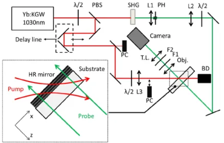
Laser damage growth experiments were carried out with the setup presented in [16] and described in Fig. 1, which has the ability to observe in situ the evolution of damage sites with high spatial resolution and to obtain time-resolved images of laser-material interactions [17].
The experiment was based on an Amplitude Systèmes laser source operating at 1.030µm and which delivered pulses with 1mJ maximum energy. Pulse durations during experiments were of 550 ± 20fs, estimated from sech2 fit of a single-shot autocorrelator measurement. The
beam was Gaussian-shaped. Most of the energy in the beam was directed to a sample and focused using a 150 mm-focus lens to perform laser damage experiments. It was called pump beam. The beam diameter in the focal plane was 65µm at 1/e at normal incidence. The pulse energy was controlled with a “half-wave plate+polarizer” system. Shot to shot energy was recorded with a pyroelectric cell set on a sample path. This energy measurement was calibrated using a removable cell set after the focusing system. Knowing both energy and spatial profile and according to ISO standards, we were able to provide shot to shot fluences in the focal plane in terms of normal beam fluences, i.e. measured in a plane that is normal to the beam axis.
A second part of the experimental setup operated at 515nm. A frequency conversion module was used to convert a small fraction (about hundredths of nanojoule) of the laser source beam into its second harmonic. The second harmonic beam, also called probe beam, was expanded, collimated and it illuminated the sample from the back of the optic. The delay
between the pump and the probe beam on the sample front face was controlled with a variable delay line (Thorlabs ODL220-FS/M) mounted on the pump beam path. The maximum delay available was about 1.5ns. The probe beam was used as a light source for in-line microscopic observations. The laser impact region on the front face of the sample was observed at normal incidence with an Olympus BX51 optical microscope equipped with a 50 × long working distance objective (Mitutoyo Plan Apo SL Infinity-Corrected Objective) and a low noise CCD Camera (PCO1600). Filters were inserted between the objective and the tube lens to block the pump beam scattering (KG3, Schott) and minimize the contribution from the broadband thermal radiation from the plasma in case such event occurs (FL514.5-10, Thorlabs).
Finally, the sample was positioned using motorized stages. Growth experiments were performed at 45° incidence, in air, on dielectric mirrors. The beam polarization on the sample, S or P-polarization, was easily selected by rotating a half-wave plate located before the lens. For each laser shot, three microscopic observations of the impact region were performed: before the pump beam irradiation, during (simultaneous pump and probe beam with controlled delay) and after.
Fig. 1. Experimental setup used for experiments. λ⁄2, half wave plates; PBS, polarizing beam splitter; PC, pyroelectric cells; SHG, BBO crystal; L1,2,3, lenses; PH, pinhole; Obj., microscope objective; T.L., tube lens; F1,2, filters; BD, beam dump. Inset on the left-hand side describes the pump-probe configuration in the sample area.
2.2. Samples and production of engineered damage sites
The studied component was a high reflective mirror made with HfO2 and SiO2. The dielectric
structure was deposited on a BK7 substrate using a PVD ion assisted e-beam evaporation process. Its design was [BK7 / (HL)^15 H 2L / Air] where H (respectively L) is a quarter-wave layer of HfO2 (respectively SiO2) at 45°. Silica and hafnia single-layers were also
coated with the same setup as control. This mirror structure operates at 45° on a spectral range centered on 1053nm. The spectral bandwidth was broad enough to work at 1030nm in both polarizations. Two identical mirrors from the same batch were considered in this process. The first one was kept intact, as a reference. The second one was prepared to manufacture engineered damage sites with a Focus Ion Beam (FIB) system. The goal was to manufacture a set of identical initial damaged structures on this mirror to perform a parametric study on laser damage growth. A motivation of this approach was the observation damage initiated from the ejection of defects embedded on such mirror, leaving pits in the stack [13]. Thus, initial structures were milled by FIB (FEI dual beam 235), equipped with a Gallium ion source pointing the sample in a vacuum chamber. An electronic source was also
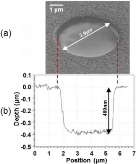
available with this system to perform in-line SEM observations without breaking the vacuum. Milled structures consisted of circular holes with a depth equivalent to the thickness of the optically neutral 2L top layer. The current used was 300 pA with an acceleration voltage of 30 kV. The structures were manufactured individually with a resolution of 20nm per point and a 50% overlap. Prior to FIB milling, the sample was coated with a thin layer of PMMA deposited by spin coating and a 10nm gold layer deposited by evaporation. PMMA acts as a sacrificial layer for the removal of the gold film that is needed for FIB structuration of the sample. After milling, the PMMA was dissolved in acetone and the samples were cleaned. The structures were post-characterized by Atomic Force Microscopy (Brucker, Dimension-Edge). In Fig. 2, we report an in-line SEM observation of the hole with the PMMA and gold layers and an AFM profile characterization realized after the milling and removal of the processing layers. The dimension of the engineering holes was 3.9µm diameter at the top of the hole and 3.3µm at the bottom and a 400nm-depth. 10 identical structures were generated.
Fig. 2. (a) In-line SEM observation of an engineered structure. Processing layers that have a marbled aspect are visible outside the hole. (b) An AFM profile characterization realized after the removal of the PMMA and gold layers.
2.3. Experimental results: LIDT characterization
We first assessed the laser damage resistance of the optical components. To that purpose, the optical setup presented in Fig. 1 was used to determine the Laser-Induced Damage Threshold (LIDT) of the mirrors. 1-on-1 experiments were performed, as described in ISO standards [6], in both linear S and P polarizations at 1030nm and 45° incidence. Results are given in Table 1. Fluences on the sample, expressed in J/cm2, were reported in terms of normal beam
fluences.
Table 1. LIDT of the dielectric mirror
Test Polarization LIDT (J/cm2)
1-on-1 S 1.37 ± 0.01
P 1.18 ± 0.01
Additionally, materials used in the interference coating were evaluated. The intrinsic LIDT (LIDT ) allows us to describe the material regardless of the beam polarization, the int
thickness of the coated layer and the angle of incidence. It uses the notion of Electric Field Intensity (EFI), which is a dimensionless quantity. The EFI is expressed by means of the following definition:
2
/ inc
EFI = E E (1)
with E ⁄ Einc the ratio of the electric field distribution to the incident field.
int
LIDT is calculated as the LIDT effectively assessed in normal beam (LIDT ) and eff
corrected by the maximum of the Electric Field Intensity (EFImax) in the sample, located
where damage actually occurs [18-20]. Thus, intrinsic LIDT is expressed with the following equation:
int max eff
LIDT =EFI ×LIDT (2)
The EFImax for a given polarization and an angle of incidence is numerically estimated
with the layer thickness and the optical index measured from the coating process. Single layers were tested in S polarization at 1030nm and 45° incidence. In situ LIDT were eff
assessed and LIDT were deduced for both materials. They are reported in Table 2. int
Table 2. Intrinsic LIDT of the silica and hafnia used in the mirror coating Test Silica single-layer LIDTint (J/cm2) Hafnia single-layer LIDTint (J/cm2)
1-on-1 1.81 ± 0.03 1.44 ± 0.02
The LIDT is a parameter intrinsic to the material, whatever the interference structure. If int
the Electric Field distribution is calculated in an entire interference structure, theLIDT at eff each point can be calculated by inverting Eq. (2) and selecting theLIDTintof the
corresponding material. Following simulations will rely on this property.
2.4. Experimental results: damage growth
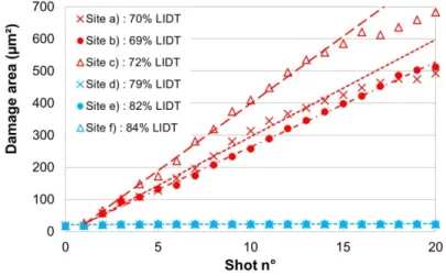
The engineered damage sites were irradiated on the experimental set-up presented in Section 2.1. Figure 3 reports the evolution of their damage areas after 1, 2, 5, 10 and 15 irradiations. These experiments have been realized for two beam polarizations (S and P) at quite the same fluence (0.95 ± 0.03 J/cm2, which is about 70% and 80% of the LIDTs in S and P
polarizations, respectively). For each polarization, we first observed that these sequences behaved quite the same which was the signature of the deterministic aspect of the growth phenomenon on HR mirror in the picosecond regime. Secondly, a difference between the two states of polarization undoubtedly appeared. Note that growth principally starts at shot #2 for each engineered hole. This late beginning is likely due to the removal of residual PMMA in the hole with shot #1. In the following text, shot #2 will thus be indexed shot #1.
Fig. 3. Repeatability. Experimental growth sequences on engineered damage sites in S polarization a), b), c) in red and P polarization d), e), f) in blue. The laser beam comes from the left of the images. Each row represents the evolution of the same site after a number of laser irradiations indicated in the top left corner of the image. The engineered damage sites are all identical: diameter 3.9µm, depth 400nm. The growth fluence is 0.95 ± 0.03 J/cm2. See
Visualization 1.
Figure 4 reports for these 6 sites the evolution of their damage areas as function of the shot number. As previously obtained on laser damage sites [14], damage areas evolve also linearly with the number of shots as followSn = × + , up to an asymptote corresponding α n S0
to the growth saturation due to the finite size of the pump beam. This saturation effect appears around the 15th shot. Experimental linear growth coefficients α are obtained from the linear regressions.
Fig. 4. Damage area evolution as a function of the shot number for the 6 sites reported in Fig. 3. Linear regressions are also reported.
They are next compared in Fig. 5 with those measured from laser damage sites on the same mirror with the same experimental conditions, i.e. that were initiated by a laser shot at a fluence higher that the 1-on-1 LIDT. Both coefficients are quite similar meaning that these engineered damage sites are representative of laser damage sites. Consequently it allows the study of the growth phenomenology in such FIB milled sites in the picosecond regime on HR mirrors.
Fig. 5. Linear growth coefficient α as a function of fluence. Comparison between results obtained on engineered damage sites (empty circles) and on laser damage sites (triangle and square) for P and S beam polarization. Intrinsic LIDT are also reported (dashed lines).
We would like to draw the reader’s attention to shot #2 (Fig. 3) for the S-polarization. Beyond damage size, a specific damage pattern is systematically observed, quite identical, made of many small damage areas arranged along concentric rings. These structures are likely due to a change in the electric field distribution in the mirror structure due to the initial damage. To investigate these effects further, time-resolved measurements were conducted.
2.5. Experimental results: time-resolved experiments
Time-resolved measurements were systematically acquired during the growth sequences. With such a configuration it is expected to observe the optical response related to the increase of free electrons density in the materials due to ionization processes, and therefore highlight the areas of energy deposition on the damage site. The time delay between pump and probe for which the maximum electrons density rose was investigated and set to 4 ps. The image sequences were then processed in order to obtain relative transmission data: intensity of the recorded time-resolved image is divided pixel by pixel by the intensity of a reference image, this reference image being taken before the laser shot. Therefore only relative variations of the transmission ratio of the laser irradiated area can be obtained, without discrimination between modifications related to change of absorption or reflection.
An example of result is given in Fig. 6 with the case of an engineered defect irradiated with S polarization at the fluence of 0.95 ± 0.03 J/cm2.
Fig. 6. (a) Example of a time-resolved acquisition on engineered damage site after the first laser shot, with probe illumination delayed 4 ps after the pump pulse. The laser beam comes from the left of the image. (b) Resulting damage morphology. See Visualization 2 for complete sequence (shot number is reported on the top-left corner).
As described previously a specific damage pattern, aligned along concentric rings, is systematically observed in the case of S polarization (Fig. 3 a,b,c – second column). The time-resolved measurements reveal a strong modulation of the transmission in this area that precisely coincides with the damage pattern location (see Fig. 6–Visualization 2). We pinpoint that these transmission modulations are directly related to the increase in free
electrons density in these location and the subsequent modification of refractive index [21]. Preferential energy deposition in such patterns could be related to modification of Electric field distribution by the initial defect. Therefore we have hypothesized that a simple modeling could reproduce the local damage occurrences. This is the topic of the next section.
3. A numerical model of damage growth
3.1. Principle of the model
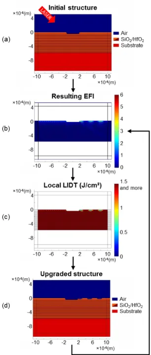
An easy way to model the engineered damage sites was to consider a hole with smooth edges and bottom on the top of a multilayer interference structure. A 2D geometry was implemented with the COMSOL software [15]. Two COMSOL plugins were used to simulate the damage growth phenomenon whose principle is summarized on Fig. 7: the radio-frequency module and the LiveLink with Matlab [22].
The first plugin uses a Finite Element Method to solve Maxwell’s equations in the frequency domain and thus calculates the Electric field distribution inside a mirror structure. The mirror structure was meshed so that the cells size in the layers was less than one-twentieth of the working wavelength. To avoid long calculation time, the total size of the 2-D geometry was limited to 20*14µm2. The algorithm simulates the propagation of an
electromagnetic plane wave incoming from the air at 45°. The laser propagation is represented in Fig. 7 (a). The incoming wave in the simulation had a uniform energy distribution. During experiments, we used a 65µm-1/e diameter Gaussian beam. At 45° incidence and inside a 20µm window, the energy distribution is almost uniform (variations lower than 5%). Thus, using a 20*14µm2 calculation window is consistent with the
experimental setup. The first step of the E-field calculation consisted in assessing the E-field distribution in a perfect and infinite mirror structure. The mirror parameters (layers thicknesses and optical indexes of HfO2 and SiO2) were identical to those of the mirror
described in Section 2. Then, this E-field was considered as a source term for the E-field calculation in the damaged structure represented on Fig. 7 (a), using a scattered field method provided by COMSOL. The damaged structure for the simulation was chosen to fit the engineered hole in terms of dimensions and depth. Perfect Matched Layers (PML) were used in order to truncate the substrate, the air and each layer of the multilayer stack (see the four rectangular borders in Fig. 7). It is a numerical concept already implemented in COMSOL that avoids reflections due to edge of the calculation window. PML thickness was set at 1030nm, i.e. the working wavelength. The EFI was calculated on each point of the structure, as shown in Fig. 7 (b). Due to the mirror design, the light does not penetrate deep in the structure (EFI goes to zero towards the substrate) and the EFI maximum values are reached in the top layers. Given this result and knowing the intrinsic LIDT of each material reported in Table 2, the effective LIDT of each point of the structure was calculated using Eq. (2). It is represented in Fig. 7 (c). In the given example, one can observe that most part of the structure withstood laser irradiation at fluence higher than 1.5J/cm2. However, some points at the right
of the initial hole showed a fluence threshold lower than 1J/cm2. One input parameter of the
model was the incident fluence. Thus, by considering an incident fluence of 1J/cm2, the part
of the structure that withstood this fluence was left unchanged whereas the other was removed. This distinction was done using Matlab function with the LiveLink plugin.
After running COMSOL radio-frequency module, we ran Matlab to express the new mirror surface as an interpolated function that modifies the optical index by setting it equal to 1 in the removed area. Finally, Matlab was used to iterate the calculation. The upgraded geometry (see Fig. 7 (d)) was used as the input geometry for a new loop, each loop thus corresponding to a laser shot. Simulations of damage growth sequences are presented in the next section.
High E-field enhancement that leads to weak local LIDT values may occur deep in the coating. One strong hypothesis in our model was that a group of elements was removed only when interfacing with the air. In this way, growth phenomenon relies on shot-to-shot
delamination. This is based on the fact that for dielectric layers, without going into details of the physical mechanism for material removal, there is a well-defined threshold for delamination in the sub-picosecond regime and that delaminated structures exhibit clean edges [23,24]. Since growth experiments were carried out at fluences close to the LIDT of the mirror, deep damage generations were avoided.
Fig. 7. Principle of the growth sequence simulation. (a) Initial structure whose hole dimensions fit engineered holes described in Section 2. (b) EFI got from the propagation of a plane wave at 45° incidence. A scattered field method is used for the calculation. Only the EFI in the mirror is represented. (c) Local LIDT in the mirror structure obtained from Eq. (2). (d) Considering an incident fluence of 1J/cm2, the part of the mirror that doesn’t withstand this fluence is
3.2. Comparison with experimental results
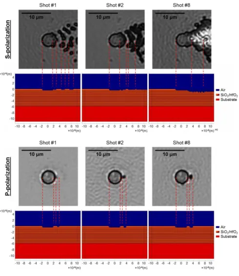
Fig. 8. . Growth sequences in S and P polarizations of an engineered damage (gray pictures) and the corresponding modeling case (color images). The red dotted lines match the damaged areas with the simulated damage morphology. Similar structures are observed in both cases.
The simulations obtained from the numerical growth model were first compared for each shot with the experimental acquisitions reported on Fig. 3.
Figure 8 reports these comparisons at shots #1, 2 and 8 for S and P polarization states, respectively. The experimental configurations and the modeling parameters were the same: angle of incidence 45°, fluence 0.95 J/cm2 which is about 70% of the intrinsic LIDT of this
mirror at this pulse length (550 fs).
In the S-polarization configuration, for the first two shots, periodical patterns corresponding to the top-layer damage are well visible in the direction of the incident beam. They are arranged along concentric semicircle spaced by undamaged area. On Fig. 8 for comparison, the red dotted lines point the correspondence between the experimental damage pattern and the localization of the local damage from modeling. The correspondence is striking; the intervals between damaged areas are well reproduced. Qiu et al. carried out calculations of the E-field distribution on mitigated damage sites and observed a similar periodical pattern [25].
For the following shots, the bottom layers are next delaminated, the delamination is observed both experimentally and from modeling. In the P-polarization configuration, despite the low growth speed, the correspondence between experiment and modeling is good again, confirming that for this mirror, the growth dynamic is much lower with the P-polarization than with the S-polarization.
An atomic force microscope (AFM) characterization of the damage at the end of the experimental growth sequence was then performed, allowing precisely measuring the damage depth and determining its morphology. The experimental profile is overlaid on the modeling result (Fig. 9) showing that the correspondence is not perfect in case of S-polarization. The experimental damage is not as deep as estimated from modeling. The correspondence is better for P-polarization, due to the fact that only the first layer is delaminated in this configuration. In order to reproduce the growth phenomenology with a better precision, a 3D modeling approach is likely necessary instead of the 2D-one. The electric field amplification is expected to be lower in this case. Also, mechanical stress was not considered in this model. However, our calculation depends highly on the structure’s geometry. This stress might slightly modify the result of the material removal and thus the successive and resulting damage morphologies. This can go toward broadening the gap between simulations and experiments. Simulation could be improved by considering the impact of mechanical stress or light scattering due to the micro-roughness on the laser growth.
Fig. 9. The damage profiles (black lines), corresponding to the damage sites at the end of the experimental growth sequence (top row), measured by means of atomic force microscopy are compared with the modeling results (color profile on the bottom row) in S and P polarizations, (a) and (b) respectively. The AFM profile in case (a) exceeds the calculation window. The blue color corresponds to the air environment and orange layers (respectively red layers) correspond to SiO2 layers (respectively HfO2 layers).
3.3. Comparison with pump-probe experiment
The main underlying hypothesis of our approach to damage growth modeling is that material is removed at the position where the local intensity exceeds some intrinsic threshold of the material. Reported time-resolved measurements have revealed that the position of energy deposition in the material, which we can directly link to the optical response of free electrons,
occurs on specific patterns. We compare in Fig. 10 the transmission modulations that have been measured with the calculated electric field distribution.
Fig. 10. (a) Time resolved acquisition on engineered damage site obtained with a probe illumination delayed 4 ps after the pump pulse. (b) Simulated EFI distribution in the interference structure. The red straight lines match the maximal local absorption with the local EFI enhancement.
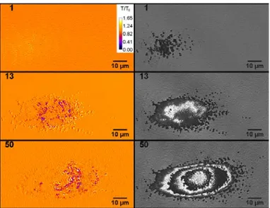
Time-resolved experiments were also conducted on laser damage sites. After the initiation, the fluence was lowered under the 1-on-1 LIDT. Images of such a time-resolved damage growth sequence are reported in Fig. 11.
Fig. 11. Energy-deposition detected with a probe illumination delayed 4 ps after the pump pulse (color images) and the resulting damage site (gray images). They are observed during growth sequence performed on a laser damage site. The laser beam comes from the left of the images. The shot number is reported on the top corner of each image. Shot #1 corresponds to the initiation of the laser damage site. For our parametric study, all the laser damage sites were initiated in P-polarization at F = 1.40J/cm2. The growth experiment has been then conducted in
These observations reveal a behavior very similar to what has been described previously: damage is growing from a strong absorption front that appears at the edge of the damage site, and which is correlated to modulation of electric field related to the damage structure. The absorption front being located at the same position from the damage edge, whatever the damage size
4. Representativeness of the study of damage growth
Foregoing results have shown that damage growth of engineered damage sites and laser damage sites are similar. Moreover a specific morphology with numerous small micrometer size damage sites is observed (see Fig. 3 and Fig. 8). Since these samples are supposed to be representative of full scale PETAL mirrors, such typical morphologies should be seen on transport mirror operating in the kJ-picosecond range on the PETAL beamline. To verify this hypothesis, microscope images of damage sites on a PETAL transport mirror were carried out after being dismantled. This large mirror was used during the PETAL 1.15 PW campaign performed in 2015/2016 and was irradiated by two laser shots only. A complete description of this campaign as well as mirror visual observation results are available elsewhere [26]. We hereafter only focus on small scale damage morphology. Figure 12 compares typical damage morphologies observed on a large PETAL mirror after operation on the facility (Fig. 12-a and c) with a representative sample after one shot on a pristine area at a fluence higher than the 1-on-1 LIDT (Fig. 12-b) and after one shot on an engineered sites at a fluence higher than the growth threshold (Fig. 12-d).
Fig. 12. Damage morphology observed on a PETAL full scale mirror after operation (a, c) and on a representative sample with engineered sites (b, d). Laser beam is coming from the left side.
Two types of morphologies are seen in both cases: small micrometer size damage with a rather high density (Fig. 12-a and b) or few micrometer damage sites with surrounding semicircle structures (Fig. 12-c and d). The former is likely to be damage sites generated at fluences higher than the 1-on-1 LIDT of the mirror, also called Intrinsic Damage Site [13], when the second is probably defect induced damage such as a nodule (structural defects of the multilayer stack related to film growth on macroscopic defects) [13,27,28] after growth (which creates the ripple pattern as shown in Fig. 8). This specific pattern has been systematically obtained in engineered damage sites as reported in Fig. 3 of Section 2.3. Since the high density micrometer damage pattern is present in both cases (large beam and small beam illuminations), we assume that this pattern is process-related. We have currently no physical interpretation to explain it. Nevertheless we confirm that large mirror under kJ-picosecond pulses and samples in damage experiments behave the same.
5. Conclusion
We have investigated the growth behavior of laser damage sites on HR mirrors at the wavelength of 1.030µm in the sub-picosecond pulse duration regime. We confirm that damage areas evolve linearly with the number of shots as follow Sn = × + as shown in α n S0
[14]. The growth coefficient α is proportional to the fluence and is modified by the polarization of the incoming beam. On the case studied, growth is very limited in P-pol whereas is more pronounced in S-pol. A COMSOL model was developed to compute the evolution of electric field distribution around the damage site during the growth sequence. Comparison between the model and experiments carried out on engineered sites and laser damage sites shows that the electric field distribution governs the growth behavior. As it’s the case for damage initiation in this pulse duration regime, growth is deterministic, imposed by material properties and electric-filed distribution. This also suggests that growth might be limited by tweaking the stack design. Damage morphology observed on samples used in this work appears to be similar to that seen on full scale PETAL mirrors. This emphasis the representativeness of the study herein detailed.
Additionally a pump probe time resolved experiment was used for the first time to image the growth sequence in the sub-picosecond regime. Observation suggests that a strong absorption appears where the electric field, and therefore electron density, is maximum. This confirms the major role of electric field distribution in the physics of growth. We also believe that this time resolved system has a great potential to better understand damage in sub-picosecond regime as it was the case for fused silica in nanosecond regime [29].
Funding