Active Sensing in Silicon-based MEMS Resonators
by
Radhika Marathe
B.S., California Institute of Technology (2009)
S.M., Massachusetts Institute of Technology (2011)
Submitted to the Department of Electrical Engineering and Computer
Science
in partial fulfillment of the requirements for the degree of
Doctor of Philosophy in Electrical Engineering and Computer Science
at the
MASSACHUSETTS INSTITUTE OF TECHNOLOGY
June 2015
c
Massachusetts Institute of Technology 2015. All rights reserved.
Author . . . .
Department of Electrical Engineering and Computer Science
May 14, 2015
Certified by . . . .
Dana Weinstein
Associate Professor of Electrical Engineering and Computer Science
Thesis Supervisor
Accepted by . . . .
Leslie Kolodziejski
Professor of Electrical Engineering and Computer Science
Chairman, Department Committee on Graduate Theses
Active Sensing in Silicon-based MEMS Resonators
by
Radhika Marathe
Submitted to the Department of Electrical Engineering and Computer Science on May 14, 2015, in partial fulfillment of the
requirements for the degree of
Doctor of Philosophy in Electrical Engineering and Computer Science
Abstract
Microelectromechanical resonators are advantageous over traditional LC tanks and off-chip quartz crystals due to their high quality factors, small size and low power con-sumption. FET-sensing has been demonstrated in resonant body transistors (RBTs) to reach an order of magnitude higher frequencies than possible with passive res-onators due to the greater sensing efficiency of FET sensing over traditional mech-anisms such as capacitive or piezoelectric sensing. This thesis explores FET-sensing in Si-based MEMS resonators with dielectric and piezoelectric materials for design of fully unreleased CMOS-integrated resonators for multi-GHz frequency applications.
Monolithic integration of Si-based MEMS resonators into CMOS is critical for commercial applications due to reduced size, weight and parasitics. A vast majority of CMOS-integrated resonators require a release step to freely suspend their vibrating structures, necessitating costly, complex encapsulation methods. This thesis proposes the development of fully unreleased resonators in CMOS using acoustic confinement structures, which may be realized without any post-processing or packaging. These di-electrically driven, FET-sensed resonators may be fabricated at the transistor-level of a standard CMOS process, and are demonstrated upto 11.1 GHz with quality factors (Q) up to 252 with footprints of less than 5 µm × 7 µm with temperature coefficients of frequency (TCF) < 3 ppm/K.
While electrostatic resonators have been primarily explored in this work due to the availability of such dielectric materials in a standard CMOS stack, piezoelectric mate-rials remain popular in commercial MEMS resonators for their high electromechanical coupling factors. Recent years have seen a push towards integration of piezoelectric materials into standard CMOS for switching and memory applications. This work explores the performance improvements arising from the integration of CMOS-ready piezoelectric materials such as AlN into a resonant body transistor. This is shown to improve transduction efficiency for low insertion losses at multi-GHz frequencies, for applications in communications to microprocessor clocking.
Thesis Supervisor: Dana Weinstein
Acknowledgments
This thesis has been and adventure and a roller coaster ride for about six years and a number of people have been responsible for guiding and encouraging me towards its completion.
First and foremost, I would like to thank my advisor, Professor Dana Weinstein, for her technical expertise, insights and infinite patience throughout the ups and downs of my graduate work. There were occasional successes and far more roadblocks but she always made sure I came out of each meeting with her with a renewed sense of optimism and direction. I sincerely thank my committee members, Professors Jeffrey Lang and Tayo Akinwande for their poignant and thought-provoking questions and excellent feedback during our interactions.
I would like to thank all my fellow inhabitants of 38-246 for intense discussions, furious calculation and simulation sessions, homework-cum-gossip sessions, and also for always being available to listen to rants about failed experiments and dysfunctional tools. I am especially grateful to Bethany Kroese, Subramaniam Sundaram, Wentao Wang and Laura Popa for providing company in lab after hours and a special thank you to Bichoy Bahr for his help with modeling and analysis.
This work was carried out in part through the use of MITs Microsystems Technol-ogy Laboratories. I would also like to acknowledge the MTL staff for their help with training and tweaking recipes, especially Eric Lim, Dennis Ward, Bernard Alamiriu, Paul Tierney and Vicky Diadiuk. I am also grateful to my fellow labrats including Matthew Branham, Mohammed Azize, Bin Lu, Jerome Lin, Winston Chern, Jamie Teherani, for their encouragement, entertainment and help with after-hours fab buddy requests throughout the fab process. I would also like to extend a special thank you to Debroah Hodges-Pabon who is truly the mother figure for all of MTL!
This work was performed in part at the Center for Nanoscale Systems (CNS), a member of the National Nanotechnology Infrastructure Network (NNIN), which is supported by the National Science Foundation under NSF award No. ECS-0335765. CNS is part of Harvard University. I would like to extend a special thanks to Nicholas
Antoniou for amazing conversations about the history of semiconductor industry and his help on Focused Ion Beam milling.
Outside of the cleanroom, I would like to thank Gilad Yahalom, Oguzhan Uyar and Danny Bankman for all their help with the CAD tools and skill coding. I am grateful to Professors Luca Daniel, Anantha Chandrakasan, Charlie Sodini, Brian Otis, Gary Fedder and Tamal Mukherjee and their students Zohaib Mahmood, Phil Nadeau, Arun Paidimarri, John Lee, Sean Yen and Kannan Sankaragomathi for our collaborative projects investigating RBTs. On the piezoelectric RBT project, I am grateful to Professors Matteo Rinaldi and Sunil Bhave and their students Yu Hui, Zhenyun Qian, Laura Fegely and Tiffany Cheng for their tips regarding fabrication of AlN-based devices. A special thanks to Valeriy Felmetsger from OEMGroup for sidewall AlN sputtering.
Outside of the workplace, I would like to thank all the great friends I have made at MIT and Harvard through MTL, Sangam, Graduate Women in EECS and the Women’s Reading Club. A special thanks to AJ, Gairik, Maria, Himanshu, Somani, Harshad, Sivaraman, Marena, Alex and Daniel. Boston would seem a lot duller and colder without you guys! A special thank you to Rohan, Natalya, Vibha and Abhijit for your support across the miles, you are the pen-pals I never had as a kid! A special thanks to my gym instructors for helping me de-stress.
This thesis was possible due to the the blind confidence shown in my abilities by my family. My parents have always made it clear that it was a waste of their time to fly halfway across the world to see me getting any degree below a PhD and this has definitely driven me to finish my research and thesis! A special thank you to my sister for being around over the last couple of years - it has been a pleasure cooking, clothes-borrowing, TV-watching, restaurant-hopping and shop-till-you-drop-ing with you! Finally, in spite of spending the last few years in the cold, frozen and (more recently) snowed-out New England area, I am grateful to my best friend and husband, Adi, who has always brought warmth and sunshine into my life.
This work was funded by IFC, DARPA Young Faculty Award. Thanks to IBM for fabrication of devices.
Contents
1 Introduction 19
1.1 The push towards multi-GHz frequencies . . . 20
1.1.1 Transduction Mechanisms in MEMS resonators . . . 21
1.1.2 Frequency scaling of passive resonators . . . 24
1.1.3 The Need for Active Sensing . . . 26
1.2 Actively sensed MEMS resonators . . . 30
1.3 CMOS Integration of Vibrating Transistors . . . 32
1.3.1 Overview of typical CMOS process . . . 32
1.3.2 Co-fabricating MEMS with CMOS . . . 36
1.3.3 RF MEMS in CMOS . . . 40
1.4 Active sensing in Piezoelectric Resonators . . . 42
1.5 Conclusions and Overview . . . 45
2 ABR-RBTs in CMOS: Design and Modeling 49 2.1 Acoustic Bragg Reflectors . . . 50
2.2 Design of Unreleased Resonator . . . 52
2.3 Finite Element Analysis . . . 54
2.4 Small Signal Model . . . 55
3 ABR-RBTs in CMOS: Experimental Results 61 3.1 RF Measurement . . . 62
3.2 Effect of Acoustic Bragg Reflectors . . . 67
3.4 Thermal stability . . . 69
3.4.1 TCF Analysis . . . 70
3.4.2 TCF Measurement and Data Fitting . . . 72
3.5 Summary and Discussion of Performance . . . 74
4 PnC-RBTs in CMOS 77 4.1 Design of PnC in CMOS . . . 80
4.2 Resonator Design . . . 83
4.3 Experimental Results . . . 86
4.4 Finite Element Modeling . . . 90
4.5 Conclusion . . . 91
5 The Piezoelectric RBT 95 5.1 Physics of Piezoelectric RBTs . . . 98
5.2 AlN as a candidate material for the piezoelectric RBT . . . 103
5.3 Design of the Piezoelectric RBT . . . 106
5.4 Finite Element Analysis . . . 110
6 Conclusion and Future Directions 117 A What determines the Q of a resonator? 121 B Constituent Equations of Piezoelectricity 125 B.1 Effective coupling coefficient . . . 127
C Butterworth-Van Dyke model 129
List of Figures
1-1 (a) Schematic of passive resonator driven and sensed capacitively with a resonance dimension L. (b) Small signal model of passive resonator showing motional RLC branch, shunt capacitors C0 and feedthrough
modeled by Cf. . . 25
1-2 Small signal model of the RBT consisting of an RLC branch model-ing the mechanical resonant system (red) and a modified transistor small signal model (blue). Lumped feedthrough parasitics (green) are modeled by Cf and rf. . . 27
1-3 Schematic showing biasing scheme for (a) Resistively sensed resonator, (b) Wheatstone bridge configuration for piezoresistive sense transducer, and (c) FET sensed resonator. In all cases, the device is biased at a total DC current I and driven using a small AC voltage vin. . . 28
1-4 (left) Scanning electron micrograph of RBT showing gate length of 500 nm and resonant dimension ∼ 1µm. (right) De-embedded frequency response of a resonant body transistor showing third harmonic reso-nance frequency of 11.7 GHz, with electromechanical Q of 1831 and piezoresistive transconductance of 22 µ S. . . 31 1-5 Scanning TEM of FEOL stack from IBM’s 45nm SOI process
show-ing adjacent FETs with stress liners, pre-metal dielectric, silicide and contacts. False coloring used [1]. . . 34 1-6 Cross-section of Intel’s 32nm process BEOL stack showing metals and
1-7 A SOI-MEMS accelerometer formed by MEMS-first creation of mi-crostructures on an SOI substrate followed by the CMOS process flow. Source: Analog Devices Inc. [2]. . . 38
1-8 Schematic of TI’s DLP showing structures in three Al layers to create a
rotating mirror display. Source: http://celluloidjunkie.com/2010/03/26/texas-instruments-on-track-with-4k/. . . 39
1-9 (left)SEM of CMOS-integrated MEMS resonator showing electrostatic actuation. (right) Frequency response showing Q > 50, 000 at 18 kHz. 41
1-10 Schematic showing fully CMOS integrated resonant body transistor formed side-by-side with transistors in a standard CMOS process. Acous-tic isolation is provided by pre-existing materials in the CMOS stack in the front and back-end-of-line. . . 43
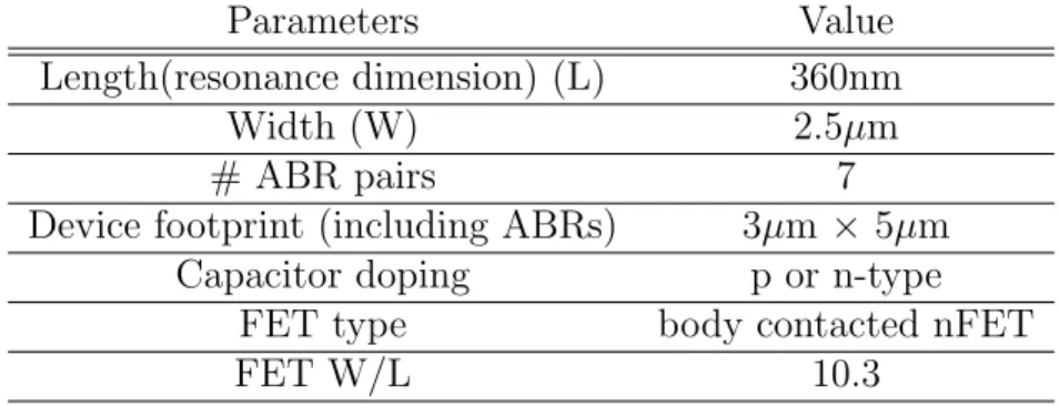
2-1 Top and 3D views of Si-based CMOS-MEMS resonator excluding acous-tic Bragg reflectors (ABRs). The resonator is driven capacitively on the left, and sensed through piezoresistive modulation of the nFET drain current on the right. Details of FET layout and doping layers are not shown. . . 50
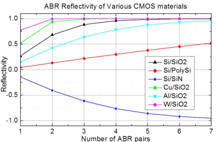
2-2 Comparison of the acoustic reflectivity of various ABR material pairs. For finite number of ABR pairs, the reflectivity increases with the number of pairs and converges to 1 or -1 rapidly for materials commonly found in CMOS. . . 51
2-3 Cross section view of resonant cavity with surrounding ABRs. The capacitive force is applied along the y-axis across the gate dielectric on the drive side of the resonator. Acoustic vibrations are excited in the resonant cavity along the x-direction through the Poisson effect and decay exponentially as a function of length along the ABRs. . . 53
2-4 3D Finite element analysis of unreleased RBT showing (a) symmetric half-plane of the 3D geometry of resonant cavity and ABRs, including the full FEOL stack materials starting with the handle wafer up to the first metal layer, (b) stress plot along the resonance direction, and (c) frequency response of simulated RBT derived from the integrated stress at the FET channel. . . 56
2-5 Augmented small signal model of the RBT consisting of: (1) an RLC branch modeling the mechanical resonant system (red), (2) a modified transistor small signal model (blue), and (3) detailed feedthrough par-asitics (green) accounting for the direct feedthrough to drain, gate and body of the transistor. . . 58
3-1 SEM of CMOS stack obtained using FIB. The resonant cavity com-prised of the SCS device layer and acoustic Bragg reflectors is seen fully buried under the metal layers. . . 62
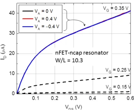
3-2 DC response of a sample device showing transistor characteristics and no dependence of drain current ID on drive capacitor voltage VA . . . 63
3-3 Frequency response of an nFET-ncap RBT showing a resonance fre-quency of 11.1 GHz with Q of 30. The drive capacitor voltage VA
modulates the gain at resonance verifying the mechanical nature of the resonance peak. . . 64
3-4 Measured response of nFET-ncap resonator at VA = 0.4V and VD =
0.6V (black) in close agreement with the equivalent small signal model (red) (Fig. 1-2). Extracted model parameters are included in Table 3.1. The model shows a good response for the primary mode, but additional spurious modes are not captured by the single LC branch. The systematic offset in the phase is the result of imperfect open/short de-embedding. . . 65
3-5 Frequency response of nFET-pcap RBT with improved feed-through relative to the nFET-ncap device. Phase at resonance agrees well with analysis (∼ 90◦). . . 66 3-6 Frequency response of a passive device with pcap drive and sense,
show-ing no discernible peak around the designed resonance frequency of 12 GHz. De-embedded S21 response using consistent open-short
struc-tures across active and passive devices is shown on a linear scale. . . . 67 3-7 Comparison of unreleased RBTs with identical resonant cavity length
but with different ABR spacing. ABR 1 is designed at the cavity resonance frequency; ABR 1.05 is designed for 5% higher frequency, while ABR 0.95 is designed for 5% lower frequency. The resonator with ABRs designed at resonance frequency shows optimized spurious mode suppression. . . 68 3-8 Simulated variations in normalized frequency and Q for RBT with
7 ABRs corresponding to percentage change in (LSi/LSiO2)). Here,
LSi is the length of Si-PolySi stack and LSiO2 is the length of SiO2
which together form one pair of ABR. The red lines mark ±10% of the designed values. . . 70 3-9 Zooming in around the measured resonance peak included in inset
shows multiple spurious modes that make up the peak. Plot com-pares measured values of the transconductance and data fitted using rational transfer functions. Measured data shown in black, red lines show the output from the rational transfer function model. . . 72 3-10 ∆f /f0 with error bars plotted against temperature. Reference lines at
±5ppm/K are shown. . . 74
4-1 (left) Cross-section view of deep trench capacitors in IBM’s 45nm SOI process showing > 35 : 1 aspect ratio. (right) Details showing the interfacing transistors along with PolySi strap connecting the capacitor through the BOX. . . 78
4-2 Cross-section schematic of a standard CMOS stack showing phononic crystal formed using BEOL layers, encapsulating resonant cavity formed in FEOL layers. . . 80
4-3 Schematic of 2D phononic crystal showing conditions for Bragg and Mie resonances which result in phononic bandgaps. . . 81
4-4 (a) Unit cell of the PnC implemented in this design (b) Irreducible Bril-louin zone showing directions of k -vector scan. (c) COMSOL simula-tion of the PnC unit cell showing bandgap a bandgap between 2.80 GHz and 6.27 GHz. . . 84
4-5 Top view of PnC resonator showing driving and sensing transistors, gates, modified contacts, first metal level and bulk ties. Metals layers are excluded for clarity of underlying structure. . . 85
4-6 (a) Cross-section SEM of a CMOS-MEMS resonators showing PnC patterned in metal stack and FEOL resonant cavity (b) details of res-onant cavity showing driving and sensing transducers. . . 86
4-7 (left) IDS− VDScharacteristics and (right) IDS− VGS of the resonator’s
sensing FET showing expected transistor response. In operation, the the sensing FET was biased at VDS = 0.6 V and VGS = 0.65 V. . . 87
4-8 Measured mechanical transconductance gm = Y21−Y12of the fabricated
PnC RBT. Measured frequency response of the PnC-RBT along with the fit generated using a 24-pole rational transfer function in MATLAB. 88
4-9 Comparative response of modified long wall-like vias used in resonator design versus regular foundry-provided square vias. The design using foundry-provided square vias shows a distorted peak with low Q along with additional spurious modes. . . 89
4-10 (a) X-stress at 2.81 GHz in 2D PnC-RBT structure showing Q of 903 with acoustic losses confined to substrate. (b) X-stress in resonant structure at 4.54 GHz with Q of 52 showing losses restricted to FEOL and substrate (c) Frequency response from 2D FEM COMSOL simu-lation of PnC resonator with resonances at 2.81 GHz (Q of 903) and 4.5 GHz. . . 92
5-1 Top-view schematic of piezoelectrically transduced Resonant Body tran-sistor. AlN piezoelectric films (dark blue) are used in place of the gate oxide for a double-gate transistor for sensing and actuation. Gates (gray) consist of metal such as molybdenum. . . 98
5-2 (left) Cross-sectional SEM of fin and trench structures in bulk Si show-ing conformal deposition of AlN and Mo films, sidewall film thicknesses are approximately 1/2 to 1/3 those at the top. (right) Sample test structure in the form of a ring, expected resonance is wineglass mode. 106
5-3 Plot showing non-linear output current for linear piezoelectrically in-duced voltage at the sensing gate. Half-wave rectification behavior is expected in the output current as the FET switches between subthresh-old and linear regimes. . . 107
5-4 Plot comparing the motional impedance RX for the Piezoelectric RBT
with passive piezoelectric devices. Top axis shows thickness of film normalized to wavelength at frequency of 5 GHz for a longitudinal mode device operating in third harmonic. . . 108
5-5 Frequency response of single-ended piezoelectric RBT showing sev-eral different resonance modes between 5 and 10 GHz. Three sam-ple mode shapes of half of the symmetric resonant structure showing the x-displacement of various resonance modes are included above the frequency response. . . 111
5-6 (left) Mode shape of differentially driven and sensed mechanically cou-pled device resonating in wineglass mode (right) Frequency response of device showing complete suppression of spurious modes. . . 113 5-7 (top left) Mode shape of differentially driven and sensed resonator in
wineglass mode (bottom left, top right and bottom right) Results from parametric sweep on suspension beam length showing highest differen-tial strain and Q around 1.2 µm. . . 114 5-8 Final layout of piezoelectric RBT devices. Fabrication was carried out
at MTL. . . 115 C-1 The Butterworth Van-Dyke model is used for modeling passive
res-onators using their equivalent RLC circuit with shunt and feedthrough parasitics. . . 130 C-2 Lumped model of a Spring-mass-dashpot system representing a
me-chanical resonator, and its equivalent electrical circuit. Source: MIT 6.777 lecture notes . . . 130 D-1 Room temperature piezoresistive coefficients in the (100) plane of (a)
List of Tables
2.1 Design parameters of CMOS-MEMS RBTs fabricated in the IBM 32nm SOI CMOS process, shown in Fig. 2-1. . . 54 3.1 Extracted small signal model paramaters for the Extracted parameters
of the equivalent circuit model (1-2) of CMOS-MEMS RBTs fabricated in the 32nm IBM SOI CMOS process. . . 65 3.2 Temperature coefficient of Young’s modulus and strain energy density
of resonator materials considered for TCF simulation. . . 72 4.1 Mechanical properties for materials in the CMOS stack . . . 82 5.1 Comparison of piezoelectric coupling coefficients of common
piezoelec-tric materials [3]. . . 96 5.2 Some options of electrode metals for Piezoelectric RBT with AlN
com-paring their longitudinal acoustic impedance Za, and resistivity ρ. . . 105
5.3 Material parameters used in final design of piezoelectric RBT. . . 116 D.1 Piezoresistive coefficients of Si at room temperature [4] . . . 137
Chapter 1
Introduction
Microelectromechanical (MEMS) resonators are advantageous over traditional LC tanks, off-chip quartz crystals, and surface acoustic wave (SAW) devices due to their high quality factors (Q), small size and low power consumption in applications such as communications, navigation, microprocessor clocking, and inertial sensors etc. These MEMS resonators can be driven and sensed using a variety of transduction mecha-nisms including electrostatic [5], piezoelectric [6], thermal [7], optical etc.
Silicon has been keenly studied as the material of choice for the design of MEMS resonators due to its abundance and inexpensiveness, and due to the development of batch-fabricated, standardized integrated circuit (IC) technologies driven by Moore’s law. The availability of high purity Si, and the development of thin film and litho-graphic microfabrication techniques result in extremely small but high-precision me-chanical structures with excellent meme-chanical properties [8]. For high frequencies of operation, especially beyond the 100 s of MHz range, Si as a material exhibits a rel-atively high intrinsic f.Q limit with orientation < 100 > as compared to materials such as quartz, AlN and routing metals [9] (see appendix A). This high f.Q limit may be explained by the fact that since Si is a semiconductor, acoustic losses due to phonon-electron interactions are minimized as compared to metals and the crys-tallinity of Si leads to low losses at grain boundaries which result in materials such as AlN. As a result, Si has been widely incorporated into both dielectric and piezoelec-tric resonators for Q-boosting and improvement in power handling capability which
is discussed further in chapter 5.
This thesis explores such Si-based MEMS resonators using dielectric and piezo-electric transduction mechanisms with active sensing for scaling to high frequencies. To this end, the motivation for scaling to multi-GHz frequencies with some poten-tial applications are discussed. Following this, the limitations of traditional MEMS transduction mechanisms for frequency scaling are considered which leads to the need for a more efficient transduction mechanism such as active sensing using field effect transistors (FETs). We then discuss with the advantages of CMOS integration for FET-based transduction mechanism with an overview of the typical CMOS process and the different ways in which MEMS and RF MEMS devices have been included in a CMOS process stack to-date. Following this, the vision for the CMOS-integrated RBTs as fully unreleased devices with acoustic isolation structures formed in the standard CMOS stack is discussed. Finally, the use piezoelectric materials in place of dielectrics is explored with such FET-based sensing for further improvements in transduction efficiency for design of low impedance filters and oscillators.
1.1
The push towards multi-GHz frequencies
With the increasing pervasiveness of wireless communication technology including smartphones and personal area networks, the overcrowding of the frequency spec-trum at low frequencies has seen a surge in demand for high-Q filters and oscillators that operate in the previously unexplored multi-GHz frequency regime. At the lower end of this spectrum, exploratory applications such as wireless personal area net-works (WPAN) and body-area netnet-works (BAN) around 2.4 GHz have been allocated frequency bands in previously unregulated high frequency bands, creating a need for frequency scaling of devices.
At higher frequencies, the Extremely High Frequency (EHF) band is designated between (30−300 GHz) in the near to far infrared regimes. Electromagnetic radiation in this band has high atmospheric attenuation due to absorption by rain and atmo-spheric gases, especially the 57 − 64 GHz band which is attenuated due to resonance
of the oxygen molecule. While this restricts communication to short distances, it is in turn useful for secure wireless local area networks (WLAN at 60 GHz) that im-prove spectrum utilization efficiency through frequency band reuse. The EHF band is also useful for mm-wave imaging for concealed weapons detection as clothing and other organic materials are transparent in certain mm-wave atmospheric windows. Furthermore, specific applications such as high-definition video links for live, high-res streaming for sports events call for a continuous scaling of resonator frequencies to the multi-GHz and THz regimes.
Below we consider the different types of MEMS resonators and transduction mech-anisms available and what is most amenable to frequency scaling.
1.1.1
Transduction Mechanisms in MEMS resonators
The transduction mechanisms used to actuate and sense vibrations in MEMS res-onators may be broadly classified into active and passive transduction mechanisms. Passive mechanisms such as dielectric and piezoelectric transduction do not involve an active element such as a transistor or a constant current bias to the device. These are usually low-power devices that apply driving and sensing voltages to the input and output terminals. Electrostatic and piezoelectric transduction are briefly discussed below as they are two of the most popular passive transduction mechanisms relevant to this work.
Electrostatic transduction
The first of these, dielectric or electrostatic transduction employs electrostatic forces to convert energy from the electrical to the mechanical domain and vice-a-versa. Consider the simple scenario of a parallel plate capacitor with capacitance C with one plate tied to ground and the other plate biased at a DC voltage VDC with a small
capacitor plates is given by: fd= 1 2 ∂C ∂x(VDC+ v jωt ac )2 =1 2 ∂C ∂x(V 2 DC+ v 2jωt ac + 2VDCvjωtac ) (1.1)
As seen from the above equation, the DC force is required to generate and amplify the force at the frequency of the AC voltage vAc and the resulting force also has a
DC component as well as a 2ω component. On the sensing side, for a DC voltage of VDC applied across the plates of the resonator, the output current is given by:
iout = VDC
∂C
∂t (1.2)
Capacitive resonators have been traditionally fabricated as air-gap devices which needed extremely narrow, high-aspect ratio trenches for high electrostatic forces for actuation and sensing [10]. However, due to the fabrication difficulties associated with deep, narrow air-gaps, along with prevalent failure mechanisms such as stiction, par-ticles lodged in gap, imperfect sidewalls etc., high-k dielectrics were explored in their place for electrostatic actuation [5]. Dielectric films not only make the fabrication easier, but also increase the mechanical driving force which is directly proportional to the relative dielectric permittivity, thus improving transduction efficiency. In such resonators, the acoustic free boundary conditions are no longer defined at the edges of the driving and sensing capacitor but the acoustic wave now extends into the di-electric material and beyond into the electrode material. A possible design tradeoff with such a design include interface imperfections, phonon-electron interactions in the conducting electrode, the stress mismatch between the thin dielectric film and the Si/PolySi body, and differing acoustic properties that may distort the resonant mode resulting in a lower Q.
Such electrostatic resonators consist either entirely of Si or PolySi with the op-tional dielectric film incorporated into the mechanical body, thus taking advantage of the cost-scaling of Si micromachining and the excellent mechanical properties of single
crystal silicon (Q > 10, 000 at 1 GHz) [9]. This has led to high-Q low-cost resonators that have been extensively explored over the past two decades. The CMOS-friendly materials used in these resonators also makes them amenable to seamless integration with integrated circuit (IC) technology [11].
Piezoelectric transduction
On the other hand, resonators relying on the piezoelectric transduction mechanism incorporate piezoelectric materials such as AlN, ZnO, PZT, quartz etc. into their body, which may be excited into mechanical vibrations through the application of an AC electric field. Conversely, mechanical strain in piezoelectric materials also result in an electric displacement field and current for sensing of resonance. The details of the piezoelectric transduction mechanism are provided in appendix B.
Historically, piezoelectrically driven resonators have been preferred over electro-static devices in commercial products due to their high electromechanical coupling coefficients resulting in a much lower insertion loss in the electrical output. One of the earliest examples of piezoelectrics used in commercial resonators is that of quartz crystals employed in microprocessor clocking circuits to generate high-Q resonance. At present, for frequencies of operation < 10 GHz, piezoelectric resonators (first SAW and now film bulk acoustic resonators or FBARs) have been successfully implemented in custom MEMS-only or MEMS-last processes which can then be wire-bonded to in-terfacing circuitry such as Avago’s FBAR technology [12].
One of the key issues with piezoelectric devices such as FBARs is the inability to manufacture devices with several different resonance frequencies on a single chip as the frequency is determined by material thicknesses, and the inherently low Q of piezoelectric materials [9]. As a solution to the former, recent years have seen numer-ous examples of contour-mode piezoelectric resonators with lithographically defined frequency. In response to the latter problem of low Q of piezoelectric resonators, efforts have been made to fabricate Si-based piezoelectric resonators to boost the Q of the overall device which is now dominated by Si [6]. Another key problem with piezoelectric resonators is that several piezoelectric materials such as quartz, PZT
etc. are not amenable to CMOS integration due to the possibility of contamination of the front end of line materials or manufacturing difficulties. However, the excellent transduction efficiency and minimal insertion loss demonstrated by these devices al-low for a commercially viable multi-chip solution, in spite of parasitics that invariably arise due to the presence of wire-bonding.
Both capacitively and piezoelectrically driven and sensed passive resonators may be modeled using a simple Butterworth-Van-Dyke model provided in appendix C (Fig. 1-1(b)).
1.1.2
Frequency scaling of passive resonators
Passive transduction schemes such as electrostatic or piezoelectric transduction have been traditionally used in the majority of MEMS resonators to date. However, as res-onators scale to higher frequencies, the out-of-band rejection of the signal with respect to the feedthrough can be severely compromised, and cannot simply be mitigated by subsequent amplifier stages.
To illustrate this effect, we consider a dielectrically driven and sensed resonator with a resonant length L whose geometry can be realized using FEOL fabrication in an SOI CMOS process (Fig. 1-1(a)). The resonator’s equivalent electrical circuit may be represented by a simple Butterworth Van Dyke (BVD) model (Fig. 1-1(b)) using an RLC branch and feedthrough parasitics. The drive and sense capacitors are modeled by C0. This model has been traditionally used to model passive MEMS
resonators and is included in appendix C.
For simplicity, we assume that all other dimensions (such as W), materials, the quality factor Q and the feedthrough capacitance Cf of such a device remain constant
while only the length of the resonant cavity L changes as 1/f where f is the resonance frequency. Thus the shunt capacitor C0 also reduces as 1/f since the non-resonant
dimension is held constant. The motional resistance Rm scales as W/C02f2 where
W is the non-resonant dimension and hence remains constant with frequency in this configuration. Meanwhile the impedances of Cm and Lm cancel at resonance. Under
Figure 1-1: (a) Schematic of passive resonator driven and sensed capacitively with a resonance dimension L. (b) Small signal model of passive resonator showing motional RLC branch, shunt capacitors C0 and feedthrough modeled by Cf.
to output reduces from > 10 dB at 100 MHz and to > 0.1 dB at 10 GHz. For such resonators, an in-line amplifier stage would indiscriminately amplify the resonance signal along with the feedthrough, thus providing no improvement in the out-of-band rejection.
One method to improve the out-of-band rejection of the resonator is by keeping the drive and sense area of such resonators constant with frequency by scaling the non-resonant dimension W ∝ f to retain the same effective shunt capacitance C0. This
leads to the overall feedthrough capacitance remaining constant at C0/2 k Cf while
Rm now scales as 1/f , leading to a constant out-of-band rejection across frequencies
for a standalone device. However, in system level integration, such resonators inter-face with driving and sensing CMOS circuits with an associated input and output impedance. At high frequencies, these large shunt capacitors C0 result in large signal
being shunted to ground through such low impedance capacitive paths. This results in strict constraints on the input and output impedances of interfacing circuits, which increases overall power consumption.
1.1.3
The Need for Active Sensing
While C0 may be constrained by interfacing circuits, active sensing provides one
so-lution to overcome the limits of out-of-band rejection by utilizing a more efficient transduction mechanism to amplify the mechanical signal before the presence of par-asitics. In active resonant devices, an active element such as a transistor is usually provided to generate a current through the device which either excites vibrations or senses them. For instance, in thermally actuated resonators, a constant current running between two terminals of the device causes resistive heating and the resul-tant thermal expansion may be used to actuate mechanical resonance [13]. On the sensing side, mechanisms such as piezoresistivity may be used to sense vibrations in resonators as the strain in the device causes a change in electron mobility and modu-lates the DC current through it [7]. The phenomenon of piezoresistivity is discussed in detail in appendix D.
The small signal equivalent circuit of a capacitively driven, piezoresistively sensed resonator is provided in Fig. 1-2 , consisting of a 1-port passive BVD model and a modified transistor pi-model. The drive capacitor is represented by C0while the RLC
components model the mechanical mass-spring-damper system of the resonator. The piezoresistive sensing is represented by a transconductance gα. The integration of such
an electromechanical amplification element into the resonant cavity enables improve-ment in the out-of-band rejection of the signal before the contribution of feedthrough parasitics modeled by the Cf and rf. This model will be further developed in §2.4.
Two types of piezoresistive sensing mechanisms may be considered for Si-based resonators in a standard CMOS process. The first involves piezoresistive sensing using a resistive element [14] while the second involves piezoresistive sensing using a FET. A detailed analysis of the performance of the FET-sensing versus resistive mech-anisms in terms of gain and noise performance was carried out by Bichoy Bahr and included in [15]. Some important results from this analysis are discussed here.
We first consider a resonant structure which is sensed using a current path defined inside the resonant body. Mechanical strain at resonance piezoresistively modulates
Figure 1-2: Small signal model of the RBT consisting of an RLC branch modeling the mechanical resonant system (red) and a modified transistor small signal model (blue). Lumped feedthrough parasitics (green) are modeled by Cf and rf.
the resistivity in the current path. The stress and strain are both proportional to the resonator excitation voltage vin. For a Si-based bulk acoustic resonator operating
around 10 GHz, the sensing resistance R is limited to a few hundred ohms due to the length of resonant cavity.
Two techniques are considered to detect the piezoresistive modulation: a) con-stant current bias b) a Wheatstone bridge
• The simplest method to detect the variation in the sensing resistance is to bias it with constant current I as shown in Fig. 1-3(a) which gives a voltage gain Av of:
Av = IRgR (1.3)
and an input referred noise PSD is considered.
v2 in= v2 on |Av|2 = 4kBT I2g2 RR (1.4)
From 1.3 and 1.4, the low voltage gain and high noise of such an implemen-tation is limited by the value of the sensing resistor which may not be in-creased arbitrarily due to area and noise considerations. Such a configuration can be considered as an equivalent current source with very small output
re-Figure 1-3: Schematic showing biasing scheme for (a) Resistively sensed resonator, (b) Wheatstone bridge configuration for piezoresistive sense transducer, and (c) FET sensed resonator. In all cases, the device is biased at a total DC current I and driven using a small AC voltage vin.
sistance, which makes current sensing by a trans-impedance amplifier (TIA) a non-feasible solution due to the small input impedance required. Furthermore, the small resistance also restricts the DC operating point of the output node to be close to ground, presenting a limitation for the direct coupling of subsequent amplification stages.
• On the other hand, in a Wheatstone bridge configuration show in Fig. 1-3(b) shows an implementation of Wheatstone bridge, biased at Vb, the voltage gain
Av of which is given by:
Av =
1
4VbgR= IR
4 gR (1.5)
where the total current consumption of the bridge I = Vb/R has been used.
Again, the input referred noise PSD is given by:
v2 in = v2 on |Av|2 = 64kBT R V2 b g2R = 64kBT I2g2 RR (1.6)
Comparing 1.3 and 1.4 with 1.5 and 1.6, it becomes clear that, for the same bias current, the voltage gain of the Wheatstone bridge sensing is lower than the constant current biasing scheme of Fig. 1-3(a) and the v2
in is higher.
vibrations. FET sensing relies on piezoresistivity as the dominant effect to modu-late the mobility of carriers along the channel and result in a small signal output current. Secondary contributions to the current modulation include modulation in channel length, threshold voltage, gate capacitance and electrostriction are omitted for simplicity from the small signal model presented in Fig. 1-2 and will be discussed in section 2.4.
Consider a resonator with the same geometry as that of the resistive sensing res-onator with the only variation being that of sense transducer. Mechanically, this device behaves identically to the resistively-sensed device and strain induced at res-onance is related to the input voltage in the same manner. The magnitude of the relative change in the FET channel mobility ∆µ/µ due to piezoresistance is equal to the relative change in resistivity, but with opposite sign. Thus, assuming the FET is biased in saturation, the voltage gain is given by:
Av = −Ir0gR (1.7)
Given the large output resistance of the FET, for the same mechanical structure and the same bias current, FET sensing thus has a voltage gain that is r0/R higher
than its resistive counterpart. For the devices considered in this work, this ratio is as high as 200.
For short channel devices, the thermal noise coefficient γ ∼ 1 and for a transcon-ductance gmF ET the input referred noise voltage PSD is given as:
v2 in = 4kBT γgmF ET I2g2 R (1.8)
Comparing the input referred noise PSD of both FET and resistive sensing, we have: v2 in|F ET v2 in|Res = γgmF ETR (1.9)
For typical designs, gmF ET is a fraction of mS, such that the input referred noise of
considered in this work, gmF ET is of the order of 500 µS, resulting in an input
re-ferred noise for the FET of only 5% that of its resistive counterpart. Additionally, the acoustic wavelengths are on the order of 100 s of nm in GHz-frequency resonators, which limits the area of the sensing resistor but does not restrict FET output resis-tance. This makes the FET more suitable for higher frequency implementations which incorporate shorter wavelengths.
The downside of FET sensing comes from its higher power dissipation as compared to resistive sensing. When biased in saturation, the sensor FET consumes more DC power than the resistive sensor. For the ABR-RBT described in this work, designed for a bias current of 60 µA, and a drain voltage of 500 mV , the FET sensing power dissipation is more than 80× larger than the resistive sensing.
1.2
Actively sensed MEMS resonators
The concept of active FET-sensing in MEMS devices has been around since Nathanson’s Resonant Gate Transistor in 1967 [16]. This resonator employed a gold cantilever sus-pended on top of a transistor channel. The voltage applied to this cantilever served as the gate voltage of this channel and any vertical motion of the cantilever modulated the capacitance and hence the output current of the transistor.
In more recent times, FET sensing has been demonstrated in Si up to 165 MHz in a double-ended tuning fork with 2 FinFETs [17] and up to 226 MHz in Si nanowire based resonators [18]. Resonant Body Transistors (RBTs) [19], [20] with internal di-electric drive and Field Effect Transistor (FET) sensing up to 37 GHz have also been previously demonstrated (Fig. 1-4). Transistor based sensing has also been demon-strated in piezoelectric GaN-based resonators, up to 2 MHz [21] and more recently , up to 3.5 GHz as switchable GaN resonators in metal-on-metal IC technology [22]. FET-sensing has thus been shown to reach order of magnitude higher frequencies than possible with passive resonators due to the decoupling of the drive and sense transduction mechanisms.
Figure 1-4: (left) Scanning electron micrograph of RBT showing gate length of 500 nm and resonant dimension ∼ 1µm. (right) De-embedded frequency response of a resonant body transistor showing third harmonic resonance frequency of 11.7 GHz, with electromechanical Q of 1831 and piezoresistive transconductance of 22 µ S.
demonstrated with suspended CNT arrays used as the gate electrode for a transistor channel, known as CNT-SGFETs. Resonance frequencies of 120 MHz have been re-ported for biological and chemical applications such as single-molecule sensing [23]. The use of GaN high electron mobility transistors (HEMTs) with mechanically float-ing carbon nanostrfloat-ings (NS) or CNTs servfloat-ing as the floatfloat-ing gate have been demon-strated for detection of THz radiation modulated by mechanical resonance frequencies in the MHz or GHz range [24].
A separate class of devices with active piezoresistive sensing comprises of various geometries such as rings [25], disks [26] and bulk mode resonators [27]. Piezoresis-tive sensing has also been demonstrated in single-walled CNTs upto 79 MHz [28], in CMOS-MEMS resonators [29] and thermally actuated resonators up to 61 MHz [7]. Such piezoresistively sensed resonators have been employed for a variety of applica-tions such as for gas recognition, pressure sensing [30] and biomolecular detection [26].
1.3
CMOS Integration of Vibrating Transistors
Due to the necessity of FET-sensed resonators for high-frequency operation, one di-rection to explore would be the design of MEMS resonators inside of the CMOS stack to access the high-performance, high-yield transistors available in the front-end-of-line (FEOL). Apart from the high yield of CMOS processes as compared to in-house, custom MEMS processes for transistor fabrication, the length scales of CMOS are also about 10−100× smaller than in-house processes due to the availability of state-of-the-art tools and processes, which allow for scaling to higher frequencies. Furthermore, the integration of MEMS resonators with the CMOS stack leads to reduced para-sitics from on-chip and off-chip routing for high frequency operation, smaller size and weight, and decreased power consumption by alleviating constraints for impedance matching networks [31], [32]. At present, a majority of electromechanical devices re-quire a release step to freely suspend the moving structures. This necessitates costly complex encapsulation methods and restricts MEMS fabrication to back end-of-line (BEOL) processing of large-scale devices in CMOS. Thus, apart from the access to high-performance transistors, development of unreleased Si-based MEMS resonators in CMOS is a critical step towards seamless integration in CMOS with no post-processing or packaging.
However, such seamless MEMS-CMOS integration presents a number of chal-lenges to the performance of the MEMS devices as well as the surrounding CMOS circuitry. Before the details of such challenges and constraints may be discussed, an overview of a typical CMOS process is presented followed by a discussion of MEMS, and specifically RF MEMS design in CMOS.
1.3.1
Overview of typical CMOS process
Due to the high cost of tools required in a state-of-the-art CMOS foundry, along with the fast turnaround times (based on Moore’s law [33]), CMOS foundries have relied on process standardization and design to deliver high-yield and reliable IC technol-ogy. While several different materials and fabrication techniques are theoretically
possible in each part of the process, the customer is typically restricted to a few re-liable designs for active and passive components whose reliability and functionality is guaranteed by the foundry. Whereas traditional CMOS processes have used bulk Si as a starting material, as the industry moves towards smaller devices, increased transistor capacitance and feedthrough has forced the introduction of Si on insulator (SOI) substrates. In an SOI wafer, the active or device layer is separated from the bulk or handle wafer by a layer of buried oxide (BOX) which helps to electrically isolate adjacent devices which in turn lowers the parasitic leakage capacitance and current to save power with the trade-off of increased substrate cost.
Regardless of starting substrate, a typical CMOS process is divided into two sec-tions, the Front-End-of-Line (FEOL) and the Back-End-of-Line (BEOL) process flow. The FEOL forms the first few layers that are manufactured in a CMOS process which typically form all semiconductor devices in a circuit such as transistors (Field effect transistors or FETs and bipolar junction transistors or BJTs), diodes, resistors, ca-pacitors (such as MOSCAPs, deep trench caca-pacitors) etc. The BEOL includes the fabrication of metal interconnects and vias along with certain passive components such as capacitors (in the form of MIMcaps) and inductors.
The key differences between the FEOL and BEOL are in terms of the materials used and the processing temperatures that result from this material choice. As a very brief description, the typical FEOL process flow involves selection of a silicon substrate, i.e. specifying starting wafer type (bulk versus SOI), orientation, doping, wafer size, wafer flatness etc. Following this, the gate regions are typically patterned along with optional shallow trench isolation (STI) structures. This is followed by the definition of active regions, p and n wells, by ion implantation. After this step, the gate dielectric and gate polysilicon/metal are grown or deposited based on the exact materials used. The gate as well as source/drain regions are defined by ion implantation. At this stage, the transistor in itself is complete but disconnected and hence the next step is that of creating silicide to connect the gate and source/drain regions to metal interconnects. Stress liners may be deposited following this step for controlling channel mobility, especially for short channel length, high-frequency
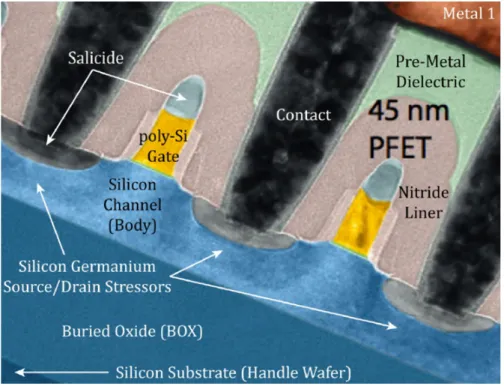
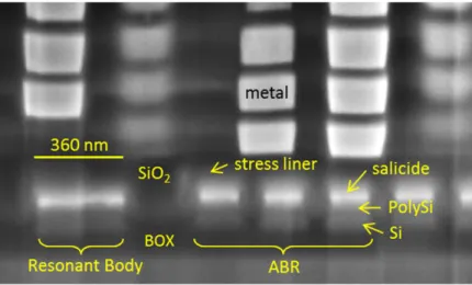
Figure 1-5: Scanning TEM of FEOL stack from IBM’s 45nm SOI process showing adjacent FETs with stress liners, pre-metal dielectric, silicide and contacts. False coloring used [1].
devices. A TEM image of the FEOL stack for IBM’s 45nm process is included in Fig. 1-5.
Thus, these FEOL processes typically use materials such as silicon in the device layer; silicon dioxide (or high-k dielectrics) as gate dielectric, or in electrical isolation structures such as the buried oxide (BOX) layer and STI; polysilicon/metal for FET gates; silicide for forming ohmic contacts; silicon nitride as stress liners etc. Temper-atures in the FEOL typically reach > 1000 C for annealing and activation of dopants, deposition of materials such as PolySi.
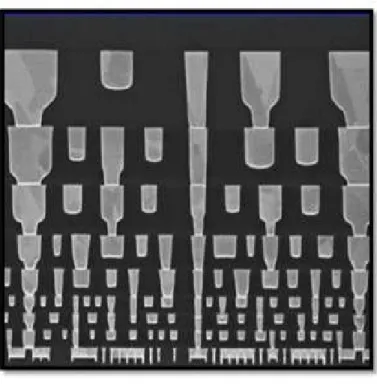
The final steps in a CMOS process, also called BEOL, involve the deposition and patterning of various levels of metal interconnects composed of metals such as Cu/W/Al, connected by vias or metals such as Cu/W and electrically isolated from adjacent connections by low-k dielectrics. Al has been traditionally used to form interconnects as Cu was not patternable through the traditional lithography and plasma etch processes due to the lack of volatile Cu compounds. The damascene or additive patterning process was devised to pattern Cu as it has better conductivity
than Al, thus reducing resistive losses. As part of the damascene process, efforts are made to planarize the metal to avoid problems with thickness of metal on non-planar topography, development of “opens” and difficulty with photolithography. Chemical Mechanical Polishing (CMP) is introduced and a certain level of via and metal pattern density is maintained to aid the planarization process. Processing temperatures are not increased beyond 450 C in the BEOL process flow to avoid diffusion of the metal layers. Fig. 1-6 shows a cross-sectional SEM of a typical BEOL stack.
It is worth noting here that a barrier metal layer is required to completely surround Cu interconnects to prevent diffusion of Cu into Si which may cause deep-level traps and compensate the dominant charge carrier type by annihilating free electrons or holes. While the thickness of this barrier metal often takes away the improvements in conductivity that Cu provides over Al by reducing its cross-sectional area, Cu brings an additional benefit over Al: electromigration resistance. Electromigration is the process by which ions are transported in a conductor due to momentum transfer between electrons and metal ions and is relevant in applications with high current densities. Cu has about 5× the electromigration/current density limit as Al due to higher electrical and thermal conductivity and melting point.
Additional details on the CMOS process flow may be found in any standard elec-tronics/CMOS fabrication textbook [34].
Typically CMOS foundries provide several rules (known as the design rule check or DRC) that dictate the permissible layout, pattern density, critical dimensions and overlap etc. to ensure high yields for the designed process. For instance, a typical design rule file does not allow for: a transistor to be formed on the same device “island” as a capacitor, only the source or the drain of a MOSFET to be populated with vias, changing the dimensions of provided deep trench capacitors, and removing dummy gate stacks etc. For the purposes of MEMS design, engineers often need to make such modifications based on the optimized mechanical design at the risk of unknown yields and compromised performance of the resulting design. MEMS designers typically need to provide a list of all DRC rules being violated by a particular design for foundry approval before the wafers may be processed to ensure
Figure 1-6: Cross-section of Intel’s 32nm process BEOL stack showing metals and vias on a background of insulating dielectric. Source: Intel.
that the yield and performance compromise does not propagate across the wafer. To this end, the DRC rules most amenable to modification include changes in layout of individual transistors, vias and routing, while those least amenable to modification include changes in pattern densities and changing dimensions of deep etches which may lead to crack propagation through the wafer. It is also noted that having several DRC modifications essentially renders it pointless - in such a scenario, it is best to create an extended DRC set for the MEMS design to catch inadvertent errors in the complex MEMS designs.
1.3.2
Co-fabricating MEMS with CMOS
The integrated CMOS process flow, originally developed for electronics, has been adopted for a wide variety of MEMS devices including imagers, inertial sensors, chem-ical and biologchem-ical sensors, actuators for switching, and filters [31]. There are several incentives for integration of MEMS with CMOS including but not limited to: reduced packaging and chip-pinout requirements, lower weight and cost as compared to
multi-chip solutions and improved shielding from electromagnetic interference. On the other hand, the drawbacks to such an integration typically present in the form of compli-cated manufacturing, increase process complexity, restricted material choice, lower yield and higher cost per wafer. Furthermore, integration can lead to compromised performance of both the MEMS and the electronics.
CMOS-based MEMS devices are broadly classified into two categories, MEMS-first devices and MEMS-last devices. The pros and cons of each approach are considered below with some examples.
MEMS-first devices
In some cases, the MEMS sequence, or most of it, is completed prior to the CMOS transistor and metal stack formation and is known as the MEMS-first fabrication sequence.
One of the first few devices fabricated in the FEOL stack include pressure sensors [35] and neural probes [36]. The pressure sensors were fabricated as micro-diaphragms which were released by anisotropic etching of the backside of a wafer [37]. In recent years, the availability of SOI wafers has enabled preprocessing wafers using DRIE and trench fill followed by planarization to create microstructures before sending wafers to the foundry. After the completion of the CMOS process, the microstructures are defined with a second DRIE process and the BOX is released (Fig. 1-7). In such cases, wafer acceptance by foundries may be an issue due to the substantial pre-processing. Also, with such an approach, transistors need to be protected during the final release step of the MEMS in HF or BOE.
More recently, MEMS-first devices have been released and encapsulated prior to the CMOS process flow using LPCVD oxide or PolySi films to seal release-etch holes, to achieve complete modularity [38]. However such a technique suffers from increased mask count and process complexity resulting from the fully independent MEMS pro-cess flow which does not take advantage of the CMOS foundry. Resonators encapusu-lated by this method have demonstrated stable performance, promising applications in timing and inertial sensing.
Figure 1-7: A SOI-MEMS accelerometer formed by MEMS-first creation of mi-crostructures on an SOI substrate followed by the CMOS process flow. Source: Analog Devices Inc. [2].
Thus, MEMS-first devices are typically designed in the front-end-of-line (FEOL) stack with access to high performance materials with a high thermal budget such as silicon, polysilicon, silicon nitride, silicon oxide and high-κ dielectrics. However, the release etch typically required by such devices at the end of the CMOS process can significantly affect the performance and yield of the surrounding circuitry while increasing overall process complexity [11].
MEMS-last devices
On the other hand, MEMS-last devices are usually fabricated in the back-end-of-line (BEOL) of the process, after the transistor stack is fabricated, making the release step easier and decreasing the overall chip footprint due to vertical stacking [2]. However, inspite of its modularity, MEMS-last processes are restricted to the BEOL material stack, comprising of low-Q porous or amorphous materials such as metals and low-κ dielectrics which intrinsically have higher thermoelastic and material losses.
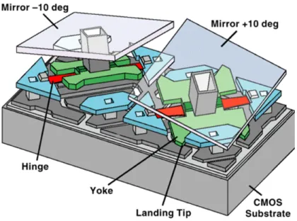
Further-Figure 1-8: Schematic of TI’s DLP showing structures in three Al layers to cre-ate a rotating mirror display. Source: http://celluloidjunkie.com/2010/03/26/texas-instruments-on-track-with-4k/.
more, the thermal budget is constrained as it has to be tolerated by the underlying electronics. While the transistors themselves can withstand thermal processing a long as the diffusion of dopants is accounted for, thermal stresses can significantly affect the resistance and electromigration limits of the metals and vias. Another constraint for BEOL processes is that conventional passivation materials such as PECVD SiN and polyimide are etched by HF, making SiO2 unusable as a sacrificial layer. Thus,
both the materials and the thermal budget limit device performance and maximum resonance frequency in MEMS-last devices.
One of the most prominent and commercially successful examples in this category of MEMS-last devices is the digital light processor (DLP) by Texas Instruments. This structure is fabricated as three layers of Al-based films for the mirror and its suspension system using resist as a sacrificial layer on top of an FEOL stack. Fig. 1-8 shows a schematic of the DLP with its hinged microstructure.
Another class of MEMS-last devices includes those fabricated on top of a complete CMOS die in a separate custom MEMS process [12], [5]. Such an approach can reduce system footprint and introduce non-CMOS materials, but is subject to increased process complexity and cost from additional masks along with the constrained thermal
budget.
1.3.3
RF MEMS in CMOS
Several RF components such as switches, high-Q inductors, variable capacitors and resonators have been integrated into CMOS in an attempt to remove off-chip bulky passives, reduce noise and scale to higher frequencies in RF architectures [39]. As one of the RF MEMS components, RF MEMS switches have been shown to have significantly better insertion loss, isolation, standby power and linearity as compared to their semiconductor counterparts such as PIN diodes and GaAs FETs [40], [41]. These are usually fabricated as post-CMOS devices in a low-temperature process and the first commercial applications have been shown by Motorola [42] and ST Microelectronics [43].
RF tunable capacitors, typically using electrothermal actuation [44], and high-Q inductors, usually as suspended structures using metallization layers [45], have also been demonstrated for applications in tunable filters, voltage-controlled oscillators (VCO) and resonators. At higher frequencies, transmission line-based resonators have been demonstrated as 37-GHz and 60-GHz multi-pole filters [46] in the form of monolithically integrated devices in a CMOS process.
The inherent resistive losses in such transmission-line based resonators limit the Q-factor as compared to mechanical resonators. Integration of mechanically vibrat-ing resonators with CMOS was first demonstrated by Nguyen and Howe fabricated using a CMOS plus surface micromachining technology [47]. An SEM of this device along with the frequency response is included in Fig. 1-9. Since then, most CMOS-integrated designs have been in BEOL processes, focused on electrostatic actuation based on the choice of materials available in CMOS. Performance improvements have been achieved by mechanical coupling to reduce feedthrough, and reduced electrome-chanical gap for high-efficiency actuation.
The FBAR commercialized by Avago may also be classified as a related architec-ture, though it is not directly integrated into CMOS technology. These resonators are fabricated as parallel-plate capacitors with a piezoelectric layer sandwiched in between
Figure 1-9: (left)SEM of CMOS-integrated MEMS resonator showing electrostatic actuation. (right) Frequency response showing Q > 50, 000 at 18 kHz.
and are assembled in a custom MEMS-first process to interface with a CMOS-VCO [48].
At this point, it is worth discussing the design tradeoffs for RF MEMS design in FEOL versus BEOL. For a fully integrated MEMS design that utilizes CMOS materials and fabrication processes, the FEOL stack provides significantly more chal-lenges that the BEOL stack in terms of design flexibility. Several design rules such as dimensions of transistor islands and gates, spacing and overlap between vias and source/drain regions, pattern densities, proximity of doping regions to transistors and isolation trenches, number and position of contacts etc. are tightly controlled in the FEOL to achieve best possible transistor performance in terms of speed, power and reliability. For instance 2-4 dummy gates are patterned at a fixed distance around the smallest gate length transistor to maintain pattern density in the gate layer and ensure accuracy in gate length fabrication. While these gates are electrically disconnected and do not affect transistor performance, they can affect the MEMS performance by changing the mode shape for a resonator designed in these layers. However, removing them is a design rule violation with risk to reliability of transistor performance. Thus, while several high-Q materials are available to the designer, DRC constraints severely restrict the design space in the FEOL.
As compared to the FEOL stack, the BEOL design rules are more flexible and restricted to via sizes, minimum spacing and minimum metal line widths (restricted
by both lithography and electromigration). One of the few constraints in the BEOL include the overlap between vias and metal lines as they are filled in a single step as part of the dual-damascene process. Overall, a much wider design space is available for patterning the materials in this part of the CMOS flow.
One approach to address the afore-mentioned challenges of integration is the de-sign of MEMS resonators in FEOL CMOS which can be realized without any post-processing or packaging. The unreleased nature of these resonators avoids extra complexity and cost, with the added benefit of increased robustness in harsh envi-ronments. In this work, IBM’s 32SOI process was chosen for its high fT transistors,
the manufacturability of small feature sizes down to < 60 nm and the presence of the buried oxide (BOX) layer for acoustic localization of vibrations in the Si device layer. Two constituent building blocks are required for the development of embedded high-frequency CMOS-integrated resonators: (i) A Si-based transducer operating ef-ficiently in the GHz frequency regime, and (ii) a solid-state mechanism to confine acoustic vibrations within the resonant cavity in a completely unreleased environment using CMOS compatible materials. The above challenges are addressed by CMOS-integrated RBTs using FET-sensing with dielectric drive and FET sensing. Acoustic isolation structures are created in the form of acoustic Bragg reflectors (ABRs) and phononic crystals (PnCs).the pre-existing layers of the CMOS stack (Fig. 1-10).
1.4
Active sensing in Piezoelectric Resonators
As transistor technology continues scaling to the deep sub-µm range driven by Moore’s Law, transistor threshold frequencies have increased, enabling transceiver circuitry to be designed in the tens of GHz range. The released and unreleased resonant body transistors discussed above [19], [20] have been explored in this thesis as candidates for side-by side integration with transceiver circuitry in a standard CMOS process using gate dielectrics for actuation and high-fT FETs for sensing. However, the impedance
of such devices is still orders of magnitude greater than those of piezoelectric de-vices due to the low transduction efficiency of electrostatic actuation as compared to
Figure 1-10: Schematic showing fully CMOS integrated resonant body transistor formed side-by-side with transistors in a standard CMOS process. Acoustic isolation is provided by pre-existing materials in the CMOS stack in the front and back-end-of-line.
piezoelectric actuation. Quantitatively, the driving forces for electrostatic actuation are 10 − 100× smaller than piezoelectric driving forces for films of the same physical dimensions, being driven with the same voltage. On the sensing side, piezoelectric films induce an additional gate voltage at the FET gate which causes a modulation in the DC drain current at resonance in addition to piezoresistive sensing, further increasing the transconductance and reducing their motional impedance [49]. As a result, devices using piezoelectric transduction with active sensing have been demon-strated in the multi-GHz range with low impedance values due to the high coupling coefficients of piezoelectric materials [17], [21].
While piezoelectric materials have not been traditionally available in standard CMOS processes, recent years have seen some push in this direction for memory and switching applications and for improvements in transistor performance. One instance of this includes GLOBALFOUNDRIES which now offers an AlN on CMOS process as a BEOL process for fabrication of MEMS and other devices. IBM’s Piezotronics effort uses the piezoelectronic transistor (PET) which is proposed as a device using a relaxor piezoelectric such as PMN-PT (lead magnesium niobate-lead titanate) in conjunction
with a piezoresistive material such as SmSe with a high piezoresistive coefficient [50], [51]. In operation, a voltage applied on the piezoelectric film induces a squeezing stress on the piezoresistive element, driving an insulator to metal transition by a change in conductivity spanning several orders of magnitude for switching applications.
Yet another application for CMOS integration of piezoelectric materials is that of memory applications using ferroelectric materials, called ferroelectric random ac-cess memory (FeRAM/FRAM) [52]. Ferroelectric materials such as BaTiO3 and lead
zirconate-lead titanate retain their polarization state after an applied electric-field is removed and this remnant polarization may be used to encode binary states in a data storage cell which has been demonstrated by shown by Texas Instruments [53] and Fujitsu [54]. More recently, ferroelectric materials have been used in negative capacitance structures stabilized by the presence of a dielectric layer with potential applications for improving transistor efficiency in the subthreshold regime [55]. Since all ferroelectric materials also show piezoelectric properties, the integration of such materials into CMOS leads to the possibility of fully CMOS-integrated piezoelectri-cally actuated and sensed MEMS resonators.
Since such piezoelectric materials are not commonplace in standard CMOS pro-cesses yet, the design and analysis of a piezoelectric resonant body transistors (which are architecturally similar to the devices from [19]) is explored in this work for an in-house process with potential for CMOS integration. Given the vision of CMOS-integration of these piezoelectric materials, high efficiency piezoelectric materials such as PZT which are not CMOS-friendly have not been considered in this work. Instead, the piezoelectric RBT in question is analyzed as a device that employs piezoelectric films such as AlN in the place of the dielectric in the configuration of an RBT. Some of the possible merits of such a configuration include:
• Improved drive and sense efficiency due to presence of high k2
ef f piezoelectric
material as compared to electrostatically driven RBT. The resulting driving forces are 10 − 100× greater than those in dielectric films of similar physical dimensions.
• Such a device with sidewall piezoelectric materials will also have higher k2 ef f as
compared to lateral drive devices due to higher value of in-plane piezoelectric coefficient. Sidewall deposition of AlN films with excellent c-axis orientation has only been demonstrated recently [56] and can be used to drive such in-plane vibrations. Overall, this results in improved Rm or insertion loss with respect
to laterally driven piezoelectric devices.
• Piezoelectric resonators fabricated with loss materials such as piezoelectrics (AlN, ZnO) and electrode materials (Mo, Al) show a reduced Q factor as com-pared to electrostatically driven devices which use low loss Si. Piezoelectric devices which incorporate Si into the resonant cavity have been demonstrated to show improved quality factor Q and power handling capability over tradi-tional designs [6]. This will be discussed further in chapter 5.
• High k2
ef f results in a large electromechanical signal in piezoelectrically
trans-duced RBTs. These devices are hence no longer restricted to small signal be-havior, allowing for non-linear behavior arising from switching of the transistor between different regimes such as cut-off, linear and saturation.
1.5
Conclusions and Overview
In conclusion, various passive transduction mechanisms such as electrostatic and piezoelectric actuation and sensing have been used in a majority of MEMS resonators to date. Such passive transduction mechanisms do not allow for scaling of these res-onators to high frequencies due to the increasing parasitic feedthrough as resonator dimensions scale down for high-frequency operation. FET-sensing using resonant body transistors or RBTs, has been recently demonstrated to reach atleast an or-der of magnitude higher frequencies than possible with passive resonators due to the presence of a more efficient sensing mechanism in the form of piezoresistive sensing in the resonant cavity. Such RBTs may benefit from integration into a standard CMOS process to take advantage of the high-fT, high-yield transistors for scaling to