HAL Id: in2p3-00124525
http://hal.in2p3.fr/in2p3-00124525
Submitted on 15 Jan 2007
HAL is a multi-disciplinary open access
archive for the deposit and dissemination of
sci-entific research documents, whether they are
pub-lished or not. The documents may come from
teaching and research institutions in France or
abroad, or from public or private research centers.
L’archive ouverte pluridisciplinaire HAL, est
destinée au dépôt et à la diffusion de documents
scientifiques de niveau recherche, publiés ou non,
émanant des établissements d’enseignement et de
recherche français ou étrangers, des laboratoires
publics ou privés.
and CsI detectors
P. Baron, E. Atkin, Y. Blumenfeld, F. Druillole, P. Edelbruck, L. Leterrier, F.
Lugiez, B. Paul, E. Pollacco, A. Richard, et al.
To cite this version:
P. Baron, E. Atkin, Y. Blumenfeld, F. Druillole, P. Edelbruck, et al.. MATE, a single front-end ASIC
for silicon strip, Si(Li) and CsI detectors. IEEE Nuclear Science Symposium and Medical Imaging
Conference - NSS/MIC 2003, Oct 2003, Portland, United States. �in2p3-00124525�
Abstract-- MATE (Must ASIC for Time and Energy) will process signals delivered from the hodoscope MUST2. The hodoscope consists of six large area telescopes (100 cm²), each made up of a double sided Si strip detector followed by a Si(Li) and Csi crystal. MATE has sixteen channels and can deliver three types of analogue information per channel; time of flight and energy loss of the detected particle; value of leakage DC current per channel. MATE also gives a trigger logical signal corresponding to the cross over of an adjustable threshold value. The analogue information is transmitted as differential current through twisted pair to the acquisition system based on VXI-C. The slow control is assured via the I2C industrial protocol. The first version of MATE for Si(strip) is available. An update of MATE will allow it to be used for the Si(Li) and Csi detectors. MATE is a novel R&D project for nuclear physics which includes both energy and time measurements with good resolution and high energy dynamic range.
I. INTRODUCTION
HE MUST2 project will allow the study of nuclei far
away from the valley of stability. It has features similar to those of MUST [1]. MUST2 consists of six telescopes (figure 1.A) that increase the solid angle coverage of MUST [1] by a factor of three. The active area of the telescope is
100cm², with position resolution of 0.7×0.7 mm2. The mass
identification is tuned for isotopes of hydrogen and helium (flight path 15 cm) and the full dynamic range is 0.4 to
45MeV. The compactness of the array (103cm3) is assured
through the use of an ASIC, which provides a significant reduction in the volume, occupied by the electronics behind the telescope, and in the number of cable /connectors leads.
The telescopes will function in vacuum at 10-6bar.
This ASIC provides the measurements of the energy and the arrival time of the particle, and will give a trigger if the energy is more than a minimum adjustable value (300keV proton for MUST2). These functionalities, the number of 16 channels and the power (28mW/Channel) offer a novel solution in front end electronic for the nuclear physic.
Manuscript received October 22, 2003.
1 CEA/DSM/DAPNIA/SEDI, CEA Saclay, 91191 Gif-sur-Yvette Cedex, France; Corresponding author: P. Baron; Email [email protected]
2 CEA/DSM/DAPNIA/SPHN, CEA Saclay, 91191 Gif-sur-Yvette Cedex, France
3 MEPHI, Department of Electronics, 115409 Moscow, Russia 4 Institut de Physique Nucléaire, IN2P3-CNRS, 91406 Orsay, France
II. THE DETECTOR MUST2
MUST2 gives the opportunity for the physic of nuclei to cover the forward and backward hemisphere simultaneously,
with a very compact hodoscope for particle γ measurements.
The distance between the hodoscope and the target has the flight distance of 15cm. The mechanics of the telescopes
(figure 1.A) is a truncated pyramid with a base 13x13cm2 and
an “active” face of 11x11 cm2.
II.A The structure of the telescope
Each telescope (figure 1.B) consists of a double-sided Si strip detector (Si(strips)), followed by Si(Li) and CsI crystals. The
dimension of the Si(strips) is 10×10cm² with 128 strips on
either face. The Si(strips) is an n-type low resistivity (~6 kOhm.cm) with a thickness of 300µm. Expected overall energy and time resolutions are 50 keV and 250 ps for alphas
of 5.48 MeV. Two Si(Li) (10×5 cm²) detectors of thickness
4.5 mm will be used to cover 100 cm². Each crystal will be segmented into 8 pads. Resolution aimed at is 120 keV and a dynamic range for protons up to 32 MeV. The CsI crystal is also segmented into 16 pads, with a thickness of 3 cm and stops 80 MeV protons. The light output is read by 4cm² photodiodes. A 6% energy resolution is expected for alphas of 5.48 MeV.
Figure 1: A) A forward (backward) tight geometry configuration. B) Exploded view of a MUST II telescope.
MATE, a single front-end ASIC for silicon strip,
Si(Li) and CsI detectors.
P. Baron
1, E. Atkin
3, Y. Blumenfeld
4, F. Druillole
1, P. Edelbruck
4, L. Leterrier
4, F. Lugiez
1, B. Paul
1,
E. Pollacco
2, A. Richard
4, M. Rouger
1, E. Wanlin
4T
Si strips Si(Li) CsI MUFEE1 MUFEE2 A BThe table 1 resumes the main specifications of the 3 detectors in capacitor, DC current and energy range values.
detector Energy Max. C detector I detector Si strips 45MeV 65pF 20nA
Si(Li) 225MeV 25pF 2uA
CsI 200MeV 130pF 10nA
Table 1: Specifications of the three detectors
II.B The structure of the electronics
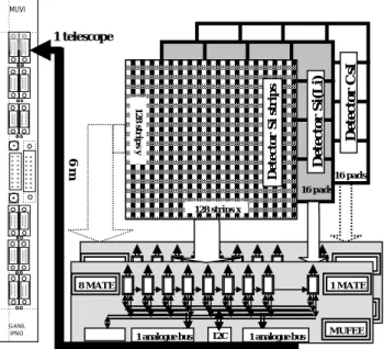
The electronic hardware of MUST II consists of three basic units, MATE, MUFEE and MUVI (figure 2). MATE is the electronic frond end of MUST2. This ASIC delivers energy and time measurements, and informs if the particle energy is greater than a minimum value. A total of 18 MATE circuits per telescope (16 for Si(strips), 1 for Si(Li), 1 for CsI) are distributed on two quasi-identical cards, called MUFEE (MUst Front End Electronics), linked to the detectors via 20 cm length Kapton bands. On these cards, we find also LVDS receiver, a sensor of temperature and a pulse generator for test and calibration. Data transfer and communication are reached through 2x25 pin connectors. A single width unit MUVI, (MUst in VXI) in VXI-C standard assures the slow control and data coding for the six telescopes.
Figure 2: the electronic of one telescope
II.C The purpose of MUST2
The purpose of MUST2 is to detect, to localize, to measure energy and identify the particle coming from interaction of the exotic nuclear beam and the target. This objective is obtained with the Si(strips). The Si(Li) and CsI are used only for energy measurement at higher energy (table 1).
The identification of the particles uses the property that their times of flight at the same energy are different (figure 3). A
good identification means good resolution in energy and in timing measurements. For example, if we consider that a minimum of 2FWHM is necessary to discriminate 2 particles, this implies, for timing (figure 4), a maximum of 910ps for
(deuteron/proton)E=6MeV, and 320ps for (alpha/ he3)E=20MeV.
2 4 6 8 10 12 14 16 18 20 22 1 2 3 4 5 6 7 8 9 10 11 12 13 14 15 16 17 18 19 20 21 22 23 24 25 Energy (MeV) Time of fligh t on 15 c m (ns) proton deuteron he3 alpha
Figure 3: the time of flight versus energy
300 500 700 900 1100 1300 1500 1700 1900 2100 2300 1 2 3 4 5 6 7 8 9 10 11 12 13 14 15 16 17 18 19 20 21 22 Energy (MeV) Timin g Reso lu tion (ps) deuteron/proton alpha/he3
Figure 4: the timing resolution versus energy for deuteron/proton and alpha/he3
III. THE ASICMATE
The design of MATE, described in this paper, concerns only the application for the Si(strips) detector. The upgrade of MATE for the Si(Li) and Csi will be described in the chapter VI of this paper.
III.A Analysis and solutions retained for MATE
Previous studies have allowed to choice between different solutions and options according to the asked specifications.
¾ Modularity: a modularity of 16 analog channels is chosen
to satisfy the minimum of power and space on the telescope.
¾ Polarity: MATE must equipped the both sides of the
Si(strips) and hence the two polarities. In the case of the junction face (entrance face), when particles between two strips, the charges created give opposite signals on the two adjacent strips [1]. To recover the data two polarities are also necessary.
1 telescope D etecto r Si s tri ps 128 strips x 128 s tr ip s y Det ecto r S i( L i) 16 pads D etect o r C sI
I2C 1 analogue bus
8 MATE 1 MATE MUFEE 1 analogue bus 16 pads MUVI GANIL IPNO ° ° ° ° ° ° ° ° ° ° ° ° ° ° ° ° ° ° ° ° ° ° ° ° ° ° ° ° ° ° ° ° °°°°°°°° °°°°°°° °°°°°°°° °°°°°°° °°°°°°°° °°°°°°° °°°°°°°° °°°°°°° °°°°°°°° °°°°°°° °°°°°°°° °°°°°°° °°°°°°°° °°°°°°° °°°°°°°° °°°°°°° °°°°°°°° °°°°°°° °°°°°°°° °°°°°°° °°°°°°°° °°°°°°° °°°°°°°° °°°°°°° 6 m
¾ Track & Hold: Coding both polarities from a single side of the detector was solved by using a track & hold instead of a peak detector for the energy channel. The signal Hold will be generated outside of the asic.
¾ Read out: Given that the counting rate is small (~0.5
kHz) a simple energy and timing read-out for all channels was adopted. This allows once more than one strip to be read.
¾ L.E.D for timing: the major difficulty is to obtain a good
resolution for time measurements. A comparative study was made between the Leading Edge Discriminator (LED) and the Constant Fraction Discriminator (CFD). It shows that the CFD gives better results over LED by a factor of 2.5 for discrimination of deuteron/proton and 4
for 4He/3He). Given the short time scale and the
performance that is requested, the LED option was chosen. LED conforms to the requirements over the energy dynamic range.
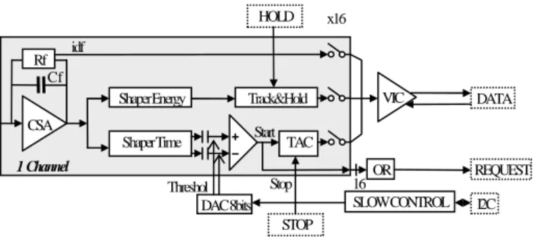
III.B Architecture of MATE
The block diagram of MATE is shown in fig. 5. The architecture is based on a modularity of 16 analog channels. The first stage of the channel is a charge sensitive amplifier (CSA) followed by energy and timing branches.
• Charge sensitive amplifier: The architecture is a
single-ended folded cascode amplifier. It is bipolar. The Rf specific block in parallel to the 3pF feedback capacitor Cf, defines the value of a 60MOhm equivalent feedback resistor, and the D.C voltage level of the amplifier output. It gives also the D.C current of the detector (250nA max.). The current is read for monitoring purposes. The rise time of the CSA is 10ns, and the gm of the PMOS input transistor is 28.38 mA/V.
• Energy: This block is composed by a shaper and a track
& hold. The shaper is composed by a CR-RC filter with 1µs of peaking time. The amplitude of the signal is memorized via a track and hold stage. The MUVI card gives the hold signal.The global transfer function of energy is +/- 15.4µV/keV.
• Timing: The timing is composed of 3 parts.
The first part is a shaper which yields the optimum filter for the best time resolution. As solution for our application, we chose a CR-RC filter for a 22ns peaking time. It has a differential structure thus giving immunity against parasitic coupling. A differential gain of 85 gives +/-568µV/keV proton at the inputs of the discriminator. The input of this shaper is connected to the CR filter of energy shaper, to avoid the offset output voltage of the CSA .Again the differential outputs are employed to the inputs of a leading edge discriminator via the CR of the time shaper. The threshold voltage is given by an internal 8 bits programmable DAC.
The second part is the leading edge discriminator. It’s composed by 2 differential bipolar stages with amplitude clipping and output differential to single-ended CMOS
translator. The main characteristics of the LED are: an input offset voltage less than 1mV, a gain larger than 5000 and a power less than 7mW. The discriminator output gives the start signal of the Time to Amplitude Converter (TAC), and the OR with the other fifteen individual start signals alerts the MUVI card that an event has been detected.
The third and last part is the TAC. It’s based on a capacitor charged by a constant current source. The full
scale is 300ns for 2.28 10 –2 % of N.L.I. The intrinsic
time resolution of TAC is 18ps FWHM. The TAC will be stopped by an external STOP signal, sent in LVPECL level to minimize timing jitter.
Figure 5: basic schematic of the ASIC
In the readout phase, the analog energy and time information of the sixteen channels will be transmitted through a Voltage to Current Converter (VIC) to the 14 bits ADC of the MUVI card. By slow control, it will be possible to read only the sixteen information of current detector. This option is useful to control the performance of the detector. The transfer function of the VIC is +/- 2mA/V per output (differential outputs). The readout frequency is 2 MHz.
The slow control of MATE (DAC for the threshold, inhibition of the channels, selection of the channel for the test, reading of the current detector) is defined and carried on the standard serial bus I2C.
For the test of MATE, an analog input can be used to inject a current signal to the input of one selected channel. It is also possible to test the sixteen TAC by sending a common exterior START signal.
III.C Energy & timing resolutions
The resolution for energy is illustrated in the fig. 6. We can see the influence of the capacitance and current detector. The theoretical resolution that we can obtain for a capacitor value of 65pF and current detector of 20nA is 16 keV FWHM.
x16
Cf
Rf idf
Shaper Energy Track&Hold
Shaper Time TAC
CSA Start 1 Channel VIC OR 16 Stop STOP DAC 8bits Threshol
SLOW CONTROL I2C
REQUEST DATA HOLD
(A) 15,9 16,1 16,3 16,5 16,7 16,9 17,1 17,3 17,5 20 30 40 50 60 70 80 Idetector (nA) re so lu ti on ( keV ) (B) 15,5 15,6 15,7 15,8 15,9 16 16,1 16,2 20 30 40 50 60 70 80 Cdetector (pF) resolutio n (keV)
Figure 6: energy resolution (A) versus I detector; (B) versus C detector For timing, the ability to separate the particles is affected by two parameters:
¾ The differential walk (difference between the time
crossing over threshold of 2 particles at the same energy), which degrades the difference of time of flight between two particles.
¾ The jitter, which degrades the possibility to differentiate
each particle.
The jitter and differential walk are illustrated in the fig. 7 for a threshold of 300keV proton. This concerns the proton and deuteron at 6MeV. The sensitivity to the value of capacitance is important. The value of differential walk is explained by the fact that the signal shape from these 2 particles is slightly different, but is negligible comparing to the 1.829ns of differential time of flight.
0 50 100 150 200 250 300 20 30 40 50 60 70 80 C detector (pF) Ji tt e r ( p s FW H M ) -300 -250 -200 -150 -100 -50 0 [t st a rt d e u te ro n ts ta rt p ro to n ] (p s) jitter diff. walk
Figure 7: Jitter & (tstart deuteron – tstart proton)E=6MeV versus C detector The ability to separate these 2 particles is illustrated in the fig.8. We have a good margin for the required detector capacitor. 5 6 7 8 9 20 30 40 5 0 6 0 70 80 C d ete cto r (p F) Numb er of FWHM
Figure 8: the power of discrimination versus Cdetector for deuteron/proton 6MeV
III.D MATE performances
All the expected performances from MATE are reported in the table 2.
Power consumption 28mW/Channel (+/- 2.5V)
Capacitance& Current of detector 65pF & 20nA
Energy
Energy max. +/-50MeV
N.L.I 3,81 10-2%
Energy resolution 16keV FWHM
Peaking time 1µs
Timing
TAC range 300ns
Time jitter (FWHM) 240ps (proton 6MeV)
Discrimination deuteron/proton 6MeV 6.5*(σFWHM)
threshold
Threshold range +/- 1MeV on 8bits DAC
Variations over all ASIC channels at 300keV +/- 10keV
N.L.I [0keV – 700keV] 0,84 %
Readout
Readout 2MHz serial
Settling time < 300ns
Table 2: the MATE performances
V TEST AND MEASURE OF ASIC MATE
The ASIC MATE was fabricated in a 0.8µm BiCMOS AMS process, and received in January 2003. The area is
6mm×6mm (fig. 9) for a number of 16000 transistors.
Given the expected performance of the ASIC, we developed a test bench with a test generator with good time and energy resolution and good energy linearity between 150keV and 60 MeV. The system has been realized around a 400000 gate FPGA and a 14 bit ADC PC integrated card. The bench allows to measure all the parameters needed to characterize the ASIC:
• I2C slow control test.
• Transfer functions of the D.C detector current.
• Phase between Hold signal and peaking time to optimize
the energy measurement.
• TAC transfer function and its resolution.
• Energy transfer function and its resolution.
• Threshold dispersion from the sixteen channels.
To be successful in the realization of the necessary test bench, we used new development method, based on UML [2]. All the results are obtained with a pulse generator, on a number of 10 ASICs. Measurements confirm a full functionality of the chip. The main performances are:
¾ Energy: a N.L.I of 0.182% (0.1% of test generator
contribution) for the dynamic range of +/-50MeV. The peaking time is 800ns and is homogeneous for all the channels (+/- 2.5%). This peaking time value is explained by the AMS process (-24% to -19.5% on the resistor value). The resolution is 20keV, and compatible with the 50keV asked for the global resolution (electronic + detector).
¾ Threshold level: the minimum value of the threshold is
150KeV. The variations over all ASIC channels at 300keV are +/-12keV (+/-30keV asked).
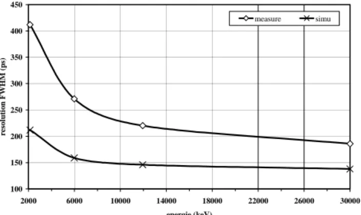
¾ Timing: for the TAC, the NLI is 0.08% on the range
80ns-300ns. The jitter of the TAC + VIC is 50ps FWHM. The total timing resolution is reported in the fig. 10. We use a pulse generator with 5ns of rise time, to know only the contribution of the electronic. The degradation can be explained by an excess of noise. Another measure gives a value of 20keV instead of 14keV for the noise at the LED inputs. We find also this problem in the energy measurement (20keV instead of 16keV). At the present time, the reason of this problem is not clearly identified and must be solved. The test with detector and source will give also some major elements to confirm the design of MATE.
100 150 200 250 300 350 400 450 2000 6000 10000 14000 18000 22000 26000 30000 energie (keV) res o luti o n F W H M (ps ) measure simu
Figure 10: timing resolution versus energy, simulation & measurement; pulse generator: 5ns of rise time; threshold level: 300keV
VI THE UPGRADE OF MATE
At the beginning of the MUST2 project, we have decided to realize the electronic frond end of the Si(Li) and Csi with discrete components. But, the constraints of power, place and number of channels (2x16) have pushed to choose an integrated solution. Studies have showed that it will be possible to use MATE, with few modifications and programmable functions:
• 3 feedback capacitors on the CSA (0.6pF for CsI; 6.6pF
for Si(Li); 2.6pF for Si(strips).
• 2 values for the energy time constant filter (1µs for
Si(strips); 3µs for Si(Li) & CsI).
• Readout of the sixteen energy information (the
information time is given by the Si(strips) detector). All these features are controlled by I2C slow control.
The main performances expected for the Si(Li) and CsI are précised in the table 3.
detector Energy Max. C& I detector Resolution energy
Si(Li) 225MeV 25pF; 2µA 77keV FWHM
CsI 200MeV 130pF; 10nA 197keV FWHM
Table 3: The main performances for Si(Li)&CsI
This upgraded version of MATE will be received at the end of October 2003. The first test of one telescope will be started at the beginning of March 2004.
VII REFERENCES
[1] Y.Blumenfeld et al, Nucl.Instr. and Meth. In Phys. Res. A 421 (1999) 471.
[2] F. Druillole, “Methodology to Measure a Front End ASIC for Physic Experiment”, Nuclear Science Symp. Portland 2003.