HAL Id: cea-02340046
https://hal-cea.archives-ouvertes.fr/cea-02340046
Submitted on 30 Oct 2019HAL is a multi-disciplinary open access archive for the deposit and dissemination of sci-entific research documents, whether they are pub-lished or not. The documents may come from teaching and research institutions in France or abroad, or from public or private research centers.
L’archive ouverte pluridisciplinaire HAL, est destinée au dépôt et à la diffusion de documents scientifiques de niveau recherche, publiés ou non, émanant des établissements d’enseignement et de recherche français ou étrangers, des laboratoires publics ou privés.
Robust ultra-thin electrografted molecular layers for
high yield vertical metal-molecules-metal junctions
Florian Lebon, Yu-Pu Lin, Hugo Casademont, Renaud Cornut, Vincent
Derycke, Bruno Jousselme
To cite this version:
Florian Lebon, Yu-Pu Lin, Hugo Casademont, Renaud Cornut, Vincent Derycke, et al.. Robust ultra-thin electrografted molecular layers for high yield vertical metal-molecules-metal junctions. ElecMol9, Dec 2018, Paris, France. �cea-02340046�
Oral preferred
Robust ultra-thin electrografted molecular layers for high yield
vertical metal-molecules-metal junctions
Lebon F.
1, Lin T.-P.
1, Casademont H.
1, Cornut R.
1, Derycke V.
1, Jousselme B.
1aLICSEN, NIMBE, CEA, CNRS, Université Paris-Saclay, CEA Saclay, 91191 Gif-sur-Yvette Cedex, France. Email :
florian.lebon@cea.fr
Abstract:
Despite the recognized potential of organic molecules for electronics, only very few types of devices (like OLEDs) incorporating thin molecular layers as active elements, have reached the level of industrial applications. Two major issues slowdown such integration: (i) the way of incorporating molecules in electronic systems is usually incompatible with device miniaturization, and (ii) thin molecular layers suffer from a limited robustness notably toward back-end process steps.
The properties of molecular layers are commonly studied using either self-assembled monolayers (SAMs) or thick non-patterned layers prepared by spin- or dip-coating. Electrografting by reduction of diazonium salts, provides an efficient alternative to these methods. It leads to robust covalent organic thin films of adjustable thickness (typically in the 5 to 50 nm range) and rich functionality. We notably showed recently that they can be used a nanodielectrics in transistors,[1] or
as active material in organic memory-based circuits.[2] These films can be assembled on all conducting
or semi-conducting electrodes, are compatible with lithography and allows the selective grafting of different electrodes of the same chip with different molecules.
However, the integration of such versatile organic thin films in functional devices requires a deep understanding and thorough control of their growth mode. In this presentation we will first present the formation of molecular thin films of controlled thickness based on two kind of diazonium salts (an insulating and an electroactive one) and then show how they can be combined in controlled double-layers for improved performances. The three different types of molecular layers were notably integrated in leakage-free large-area (>100 µm2) vertical metal-molecules-metal junctions and their
electronic performances were evaluated.
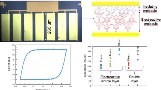
Figure 1. Final sample obtained for electrical measurements (top). Electrical measurement at 1500 Hz for one electrode (bottom left). Capacitance results for various layers (bottom right).
[1] H. Casademont, L. Fillaud, X. Lefèvre, B. Jousselme, V. Derycke, J. Phys. Chem. C, 2016, 120, 9506−9510 [2] Y.-P. Lin, C.H. Bennett, T. Cabaret, D. Vodenicarevic, D. Chabi, D. Querlior, B. Jousselme, V. Derycke, J.-O. Klein, Scientific Reports, 2016, 6, 31932.