Publisher’s version / Version de l'éditeur:
Journal of Vacuum Science and Technology A, 22, May 3, pp. 870-873, 2004
READ THESE TERMS AND CONDITIONS CAREFULLY BEFORE USING THIS WEBSITE. https://nrc-publications.canada.ca/eng/copyright
Vous avez des questions? Nous pouvons vous aider. Pour communiquer directement avec un auteur, consultez la première page de la revue dans laquelle son article a été publié afin de trouver ses coordonnées. Si vous n’arrivez pas à les repérer, communiquez avec nous à PublicationsArchive-ArchivesPublications@nrc-cnrc.gc.ca.
Questions? Contact the NRC Publications Archive team at
PublicationsArchive-ArchivesPublications@nrc-cnrc.gc.ca. If you wish to email the authors directly, please see the first page of the publication for their contact information.
NRC Publications Archive
Archives des publications du CNRC
This publication could be one of several versions: author’s original, accepted manuscript or the publisher’s version. / La version de cette publication peut être l’une des suivantes : la version prépublication de l’auteur, la version acceptée du manuscrit ou la version de l’éditeur.
For the publisher’s version, please access the DOI link below./ Pour consulter la version de l’éditeur, utilisez le lien DOI ci-dessous.
https://doi.org/10.1116/1.1651545
Access and use of this website and the material on it are subject to the Terms and Conditions set forth at
Excimer laser annealing of p-type perovskite thin films
Du, Xiaomei; Dubowski, Jan; Post, Michael; Wang, Dashan; Tunney, Jim
https://publications-cnrc.canada.ca/fra/droits
L’accès à ce site Web et l’utilisation de son contenu sont assujettis aux conditions présentées dans le site LISEZ CES CONDITIONS ATTENTIVEMENT AVANT D’UTILISER CE SITE WEB.
NRC Publications Record / Notice d'Archives des publications de CNRC:
https://nrc-publications.canada.ca/eng/view/object/?id=35c2bb86-388c-4e11-a08f-d02bcbadfaa8 https://publications-cnrc.canada.ca/fra/voir/objet/?id=35c2bb86-388c-4e11-a08f-d02bcbadfaa8
X. Dua)
Institute for Chemical Process and Environmental Technology, National Research Council of Canada, Ottawa, Ontario, Canada K1A 0R6
J. J. Dubowski
Department of Electrical and Computer Engineering, Universite´ de Sherbrooke, Sherbrooke, Que´bec, Canada J1K 2R1
M. Post, D. Wang, and J. Tunney
Institute for Chemical Process and Environmental Technology, National Research Council of Canada, Ottawa, Ontario, Canada K1A 0R6
~Received 13 October 2003; accepted 5 January 2004; published 17 May 2004!
The ability of excimer laser irradiation to anneal and to crystallize amorphous films of the p-type perovskite SrFeyCo12yO2.51x(y 50.5) has been investigated. The films were prepared by the pulsed laser deposition technique on Si and sapphire substrates held at room temperature or 240 °C. Both film deposition and film annealing were carried out using a KrF excimer laser ~l5248 nm!. Films of SrFe0.5Co0.5O2.51x deposited at room temperature on sapphire substrates have been crystallized with 160 laser pulses at 50 mJ/cm2, while irradiation of a film deposited at room temperature on a Si substrate has resulted in its crystallization following 40 pulses at 100 mJ/cm2. Films deposited at 240 °C have been crystallized with 480 and 320 pulses at 50 and 60 mJ/cm2, respectively. The application of the excimer laser annealing technique permits the modification of film crystallinity after deposition, and because this can be achieved with a high degree of control of irradiation energy, this facilitates the integration of crystalline films of high melting temperature perovskites with substrates which have a low melting point.
@DOI: 10.1116/1.1651545#
I. INTRODUCTION
Strontium iron cobalt oxide perovskite SrFeyCo12yO2.51x films have been demonstrated to be promising gas sensor materials of the conductometric family.1,2These compounds are p-type semiconductors and are nonstoichiometric in oxy-gen. For these materials, the oxygen nonstoichiometry range can be as high as 0.0<x<0.5, depending on y, and for T .350 °C reversible uptake of oxygen can readily occur.1The end member phases for these compounds are the orthorhom-bic brownmillerite form at x;0 and cuorthorhom-bic or pseudocuorthorhom-bic perovskite at x.0.4.
The electrical and gas sensing properties of the films are strongly dependent on cation and oxygen stoichiometries and on morphological structure.2However, both the structure and the morphology of the films are dependent upon deposition temperature. Previous studies have also shown that films de-posited at different temperatures have varying degrees of crystallinity and preferential orientation.3 Films prepared on single-crystal (11¯02) sapphire at 630 °C are preferentially oriented ~200!, whereas those grown above 730 °C are pref-erentially oriented ~110! as shown by x-ray diffraction. Films grown below 470 °C show no evidence of any type of pre-ferred texture or crystallinity. Films which exhibit no crys-tallinity or texture show limited sensor functionality and can-not easily reversibly change from the brownmillerite to the cubic perovskite structures.4 Thus, depositions at high tem-peratures (T.700 °C) favor the formation of textured films
which possess the desired sensor qualities of functionality. However, the high deposition temperature is a condition which is particularly unfavorable when attempting growth and integration of such perovskites upon low melting point materials, such as plastics or silicon-based substrates with integrated complementary metal oxide semiconductor ~CMOS! electronics and photoresists.
Hence, low-temperature deposition of these films is ben-eficial for applications where specific device microstructure or properties of substrates prohibit high-temperature treat-ment. Recently, it was shown that it was possible to grow crystallized SrFeO2.51x films at room temperature by pulsed laser deposition using an off-axis geometry and through care-ful control of the Ar gas pressure.5Alternately, excimer laser annealing has the potential to crystallize amorphous films,6 – 8 thus it offers another solution to this problem. Other recent studies show that an excimer laser can be used to modify the morphology of bulk high-temperature oxides6 and SrFe0.5Co0.5O2.51x films,9 and recrystallize crystalline films.10,11This study reports the use of excimer laser anneal-ing for crystallizanneal-ing amorphous films of SrFe0.5Co0.5O2.51x grown on single-crystal sapphire (11¯02) or single-crystal Si ~111! substrates.
II. EXPERIMENTAL DETAILS
The SrFe0.5Co0.5O2.51x target was prepared by conven-tional ceramic preparation techniques. SrCO3, Fe2O3, and Co3O4powders ~.99.9% pure on a metal basis! were mixed and ground together in the required quantity, followed by
a!
heat treatment at 1100 °C under oxygen atmosphere. The sample was ground up again and characterized by x-ray dif-fraction ~XRD!. Once the single-phase product was obtained in powdered form, the powder was pelletized and sintered at 1150 °C in oxygen. After XRD analysis confirmed the pellet to be single phase, the pellet was used as the target material for the deposition of SrFe0.5Co0.5O2.51xfilms by pulsed laser deposition ~PLD!.
The SrFe0.5Co0.5O2.51x films were deposited by the PLD technique on (11¯02) sapphire and ~111! Si substrates using a Lambda-Physik LPX305i excimer laser operating with Kr/F at 248 nm and a PLD setup described earlier.3 The pulse duration was about 25 ns. A series of three films was pre-pared. Films 1 and 2 were fabricated on sapphire and film 3 on Si substrates. The substrates were held at either room temperature ~films 1 and 3! or 240 °C ~film 2!. For compari-son purposes, a crystalline film was also deposited onto a sapphire substrate at T5650 °C. All depositions were car-ried out under a background oxygen pressure of 100 mTorr. The films, typically 200 nm thick, were fabricated by ablat-ing a SrFe0.5Co0.5O2.51x target with the laser operating at 8 Hz and delivering pulses with an energy fluence of 1.5 J/cm2. The average deposition rate was 10 nm/min.
Laser annealing was carried out with the same KrF exci-mer laser operating at 4 Hz. An area of 737 mm2 of the sample was irradiated with a fly-eye homogenized beam de-livered through a Microlas optics system. The irradiation was carried out in an ambient atmospheric environment with up to N5960 pulses, each delivering a fluence of 50–100 mJ/cm2. The crystallinity and grain properties of SrFe0.5Co0.5O2.51x films before and after annealing were characterized by both XRD and transmission electron mi-croscopy ~TEM!. All XRD measurements were performed on a Bruker D8 diffractometer equipped for parallel beam ge-ometry with primary and secondary double Go¨bel mirrors using a step size of 2Q50.04° with a dwell time of 2 s/step. The TEM image and diffraction were obtained using a Phil-ips CM20 electron microscope equipped with an Oxford In-struments Energy Dispersive x-ray spectrometer ~Link exl II! and a Gatan UltraScan 1000 CCD camera.
III. RESULTS AND DISCUSSION
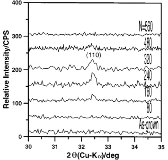
Figure 1 shows a series of XRD spectra obtained for as-grown film 1, and for the same film following its irradiation with a different number of pulses at the fluence of 50 mJ/cm2. The progress of crystallization is indicated by the development of a diffraction peak at 2Q532.4° @reflection ~110! based on the cubic perovskite lattice# which has been observed for the film irradiated with 160 pulses. However, for N>480, the film material starts to decompose; at 560 pulses, the film was ablated from the substrate surface. At a higher fluence of 60 mJ/cm2, film 1 was ablated after 80 pulses.
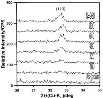
Figure 2 shows a series of XRD spectra obtained for as-grown film 2 and after annealing at 50 mJ/cm2with a differ-ent number of pulses. The film starts crystallizing at 480 pulses and the evidence of its improved crystallinity has been
observed for up to 800 pulses. The position of the ~110! reflection which developed in this film is 2Q;32.8°, which is slightly higher than that for the room-temperature grown film ~compare Fig. 1 and Fig. 2!. A shift to higher 2Q is due to a decrease in the unit-cell volume, which for nonstoichio-metric perovskites such as SrFe0.5Co0.5O2.51x is caused by the increasing oxygen content.2
Figure 3 shows a series of the XRD spectra obtained for film 2, which was irradiated with pulses at 60 mJ/cm2. It can be seen that the film has partially crystallized following irra-diation with 320 pulses. At 800 pulses, the crystal quality of the film appears to be maximized. Some decomposition
FIG. 1. XRD spectra of a SrFe0.5Co0.5O2.51xfilm grown at room temperature
on a sapphire substrate ~film 1! and annealed at a fluence of 50 mJ/cm2.
N5number of pulses.
FIG. 2. XRD spectra of a SrFe0.5Co0.5O2.51x film grown at 240 °C on a
sapphire substrate ~film 2! and annealed at a fluence of 50 mJ/cm2. N5number of pulses.
871 Duet al.: Excimer laser annealing ofp-type perovskite thin films 871
probably took place for a higher number (N.800) of irradi-ating pulses, as evidenced by a weaker ~110! XRD peak. Also, the position of that peak appears shifted to near 2Q;32.5°.
Figure 4 compares the XRD spectra for a SrFe0.5Co0.5O2.51x film deposited at 650 °C and the film de-posited at 240 °C ~film 2! after irradiation with 800 pulses. This shows that the ~110! cubic perovskite reflections are present in both films and are not significantly shifted, indi-cating that the same cubic perovskite phase has been induced in the low-temperature grown film by annealing it with the excimer laser.
The full widths at half maximum of the ~110! peaks shown in Fig. 4 were 0.16 degrees 2Q for the film deposited at 650 °C ~a! and 0.33 degrees 2Q for the film deposited at 240 °C and irradiated with 800 pulses at a fluence of 60 mJ/cm2~b!. This line broadening is caused mainly by de-creased crystallite size. Since reduced crystallite size and/or nanostructuring of metal oxide films can greatly enhance the sensitivity of gas sensor materials,12–14this suggests that la-ser annealing offers an attractive method to tailor the crys-tallite size and nano/microstructure of metal oxide films for improved performance.
Figure 5 shows TEM bright field ~BF! micrographs with diffraction patterns of film 3 as-grown on Si ~111! at room temperature and the same film following irradiation with 40 pulses at 100 mJ/cm2. It can be seen that the as-grown film possesses amorphous structure with a domain size ;10 nm @Fig. 5~a!#. After laser annealing, the film was crystallized as illustrated by the selected area electron-diffraction pattern @Fig. 5~b!#. According to the indexed pattern the crystallized film has the same crystal structure as SrFe0.5Co0.5O3~Powder Diffraction File, card 46-0335, Joint Committee on Powder Diffraction Standards! with a cubic unit-cell parameter of a 50.385 74 nm and a grain size of 30<d<40 nm. This result indicated that the film could be crystallized by a small num-ber of pulses with a higher fluence, and without evidence of damage due to ablation.
Comparing the annealing results of film 1 and film 2 using different laser fluences, it is apparent that the film deposition temperature has an influence on post-laser-annealing effects. A film deposited at 240 °C is more stable than one deposited at room temperature. At the same fluence of 50 mJ/cm2, the 240 °C deposited film needs more pulses to be crystallized. However, when the fluence was increased from 50 to 60 mJ/cm2, the film deposited at room temperature was ablated after only 80 pulses, while the film deposited at 240 °C was stable. As shown by comparing Fig. 2 and Fig. 3, it is clear that film 2 was crystallized with fewer pulses at a fluence of 60 mJ/cm2 than at 50 mJ/cm2.
IV. CONCLUSIONS
It is demonstrated that radiation from a KrF excimer laser can be used to produce a crystalline product by annealing
FIG. 3. XRD spectra of a SrFe0.5Co0.5O2.51x film grown at 240 °C on a
sapphire substrate ~film 2! annealed at a fluence of 60 mJ/cm2
. N5number of pulses.
FIG. 4. XRD spectra of a SrFe0.5Co0.5O2.51xfilm ~a! deposited at 650 °C and
~b! deposited at 240 °C and irradiated with 800 pulses at a fluence of 60 mJ/cm2.
FIG. 5. TEM image and selected area electron diffraction patterns of a SrFe0.5Co0.5O2.51xfilm ~a! deposited at room temperature on a Si substrate,
amorphous SrFe0.5Co0.5O2.51x films. Room-temperature de-posited SrFe0.5Co0.5O2.51x films on sapphire have been crys-tallized with 160 pulses at 50 mJ/cm2. The irradiation at 60 mJ/cm2with N580 pulses resulted in ablation of such a film. However, a film deposited at room temperature on a Si sub-strate has been crystallized with 40 pulses at 100 mJ/cm2. The film deposited at 240 °C has been crystallized with 480 and 320 pulses at 50 and 60 mJ/cm2, respectively. For a larger number of pulses (N.800), the XRD data indicate that some deterioration of the film crystal structure takes place. These results demonstrate the potential of the excimer laser-induced crystallization of amorphous SrFe0.5Co0.5Ox
films grown at temperatures compatible with fragile micro-structures, such as plastics or silicon-based substrates inte-grated with CMOS electronics and photo resists.
1J. J. Tunney, M. L. Post, X. Du, and D. Yang, J. Electrochem. Soc. 149,
H113 ~2002!.
2
J. J. Tunney, P. Whitfield, X. Du, and M. L. Post, Thin Solid Films 42, 221 ~2003!.
3B. W. Sanders and M. L. Post, Mater. Res. Soc. Symp. Proc. 285, 427
~1993!.
4
B. W. Sanders, J. Yao, and M. L. Post, Mater. Res. Soc. Symp. Proc. 343, 463 ~1994!.
5Z. Wang, T. Sasaki, N. Koshizaki, J. J. Tunney, and M. L. Post, Thin Solid
Films 437, 95 ~2003!.
6H. Azuma, A. Takeuchi, T. Ito, H. Fukushima, T. Motohiro, and M.
Yamaguchi, Sol. Energy Mater. Sol. Cells 74, 289 ~2002!.
7H. Tomita, Y. Nimomiya, A. Ito, and M. Obara, Proceedings of the 8th
IEEE Laser and Electro-optics Society Symposium, 1995 ~IEEE, New York, 1995!, Vol. 1, 304 –305.
8
T. Zhu, Y. P. Zhou, and Z. G. Liu, Mater. Sci. Eng., B 89, 390 ~2002!.
9
X. Du, J. J. Dubowski, M. L. Post, and J. Tunney, Opto Canada, SPIE Regional Meeting on Optoelectronic, Photonics, and Imaging, Ottawa, Ontario, May, 2002, unpublished results.
10A. Ishii, Y. Takano, S. Arisawa, and T. Hatano, Physica C 372–376, 600
~2002!.
11D. Shye, B. Chiou, C. Hwang, C. Jaing, H. Hsu, J. Chen, and H. Cheng,
Jpn. J. Appl. Phys., Part 1 42, 1680 ~2003!.
12
C. Xu, J. Tamaki, N. Miura, and N. Yamazoe, Sens. Actuators B 3, 147 ~1991!.
13
N. Yamazoe, Sens. Actuators B 5, 7 ~1991!.
14N. Barsan and U. Weimer, J. Electroceram. 7, 143 ~2001!.
873 Duet al.: Excimer laser annealing ofp-type perovskite thin films 873