Characterization of LOCOS and Oxidized Mesa
Isolation in Deep-Sub Micrometer SOI NMOS
Processes
by
Jeffrey Wade Thomas
Submitted to the Department of Electrical Engineering and Computer Science in partial fulfillment of the requirements for the degree of
Master of Science in Electrical Engineering and Computer Science at the
MASSACHUSETTS INSTITUTE OF TECHNOLOGY May 1995
© Jeffrey Wade Thomas, MCMXCV. All rights reserved.
The author hereby grants MIT permission to reproduce and distribute copies of this thesis document in whole or in part, and to grant others the right to do so.
A uthor. ... ... .. . ... ...-.:.... Department of Electrical nginer g d Computer Science May 23, 1995 Certified by... ... . . ...
'X es E. Chung Assistant Professor of Elect cal Engineering Certified by ... ... ...
Craig L. Keast Director of Micru Ietroniqs I rftory, Lin$gyn Laboratory Accepted by... ... r----... ".. V V ...
,.R. Morgenthaler Chairman, Departr ent Committee on Graduate Students
MASSACHUSETTS INSTITUTE OF TECHNOLOGY
JUL
171995
LIBRARIES
Characterization of LOCOS and Oxidized Mesa
Isolation in Deep-Sub Micrometer SOI NMOS
Processes
by
Jeffrey Wade Thomas
Submitted to the Department of Electrical Engineering and Computer Science on May 23, 1995, in partial fulfillment of the
requirements for the degree of
Master of Science in Electrical Engineering and Computer Science
Abstract
Device isolation is a very important component of VLSI manufacturing. In this work, an
NMOS process and isolation test structures and devices were designed to characterize LOCOS and Oxidized Mesa isolation for use in SOI technology. For LOCOS, the key
variables were the field-implant dose, stress-relief oxide thickness, field-oxidation time/thickness, silicon-film thickness, and field spacing. The four latter variables control the extent of lateral encroachment and stress-related oxidation effects. These parameters along with the field-implant dose, effectively controithe extent of lateral isolation and its effects on devices. The sidewall implant dose and oxidation thickness, which control 2-dimensional charge sharing effects at mesa corners and the existence of parasitic devices, were the variables of interest for Oxidized Mesa isolation. Focusing on thin films, substrates with top layer silicon film thicknesses of 50nm and 90nm were used to fabricate arrays of isolation islands, diode structures, sidegating structures, and transistors of varied dimensions and geometries. LOCOS characterization began with the testing of and performing data analysis on the isolation islands to quantify design constraints on isolation in terms of leakage. Hoand and Colinge suggested that top layer silicon film thicknesses 2 150nm necessitated excessive oxidation times to achieve complete isolation[12,14]. Results showed this phenomenon not to exist with top layer silicon film thicknesses of 90nm and below, and presented in design space graphs defining allowable process and structure parameters leading to effective isolation.
Thesis Supervisor: James Chung
Title: Assistant Professor of Electrical Engineering Thesis Supervisor: Craig Keast
Acknowledgments
I would like to express my deepest gratitude to Professor Jim Chung and Dr. Craig Keast for supervising this project, imparting your knowledge of the subject on me, and unknowingly giving me the ever so timely words of encouragement. Thanks to the staff of the Microelectronics Laboratory, Lincoln Laboratory for your patience in enduring the many questions which arose while learning my way around the clean room as well as when doing this thesis work. A special thanks to Dick, Bernie, Doug, Sandy, Kevin, Jim, Sue, Andy, Gwen, Bruce, Debbie, Bob, Jeff, and Johanna of Groups 87 and 23 for your added support. Gratitude also goes out to Jim's research group on campus, Eric, Jeff, Huy, Rajesh, Jung, Jee-Hoon, Jocelyn, Wenjie, and Ben for making my transition back to campus as smooth as possible. You all were a great help.
Special thanks to the Black Graduate Student Association, BGSA, the staff of the Graduate office, and my other friends for being my family away from home and giving me the distractions which forced me to keep the much needed balance. Many thanks to my very close friends, Dee, Don, Nadine, Araba, Rob,,Pennis, LaCreis, Matt, Andy, Daniel, Nicole, Cheryl, Sheree, Sylvester, and Amy.
Last, but certainty not least I would like to give a very special thanks to my family and loved ones for the emotional support you displayed since day one back in September, 1993. With the support and love from you that reached Massachusetts from Virginia, my stay was bearable. I dedicate this thesis to you, Betty, William, Deena, LaVerne, Kimberly, and Victor.
Contents
1 Background
1.1 Isolation Characteristics ... 9
1.2 Bulk CMOS Isolation Technologies ... 11
1.3 SOI Isolation Technologies ... 13
1.4 Project Motivation ... 15
1.5 Organization of Thesis ... 16
2 Test Structures/Devices Design
2.1 Introduction ... ... 192.2 Isolation Islands ... 19
2.3 Sidegating Structures ... 22
2.4 Comb Diodes ... 24
2.5 NMOS Transistors ... 26
3 Fabrication of Test Structures and Devices
3.1 Introduction ... 323.2 Process Parameter Splits ... 32
3.3 CAFE ... 35
3.4 Process Flow ... 36
3.4.2 Device Process Flow ...
4 Simulation of LOCOS Field Oxidations
4.1 Introduction ...
4.2 TSUPREM-4 ...
4.3 Simulation Procedure ...
4.4 TSUPREM-4 Oxidation Models ...
4.4.1 Oxidation Theory ...
4.4.2 COMPRESS Model ...
4.4.3 VISCOUS Model ...
5
Testing & Results
5.1 Introduction ... 5.2 Testing ... •... 5.2.1 Focus ... 5.2.2 Setup ... 5.3 Results ... 5.3.1 TsiEffects ... 5.3.2 SRO Effects ... ... 5.3.3 Spacing Effects ... 5.4 TSUPREM-4 Comparisons ... ... 37 ... 62 ... 62 ... .... ... .62 ... 62 ... 63 ... 64 ... 67 ... 70 ... 72
6 Conclusion
6.1 Introduction ... 74 ......
...
...
...
6.2 Summary of Results ... 74 6.3 Future Work ... 75
References
76Appendix A
78
Appendix B
90
Appendix C
107List of Figures
1 Process Description for LOCOS Isolation ... 17
2 Process Description for Mesa Isolation ... 17
3 Process Description for Oxidized Mesa Isolation ... 18
4 Process Description for REM Isolation ... 18
5 Two Finger Isolation Structure ... 27
6 Interdigitated Fingers Isolation Structure ... 28
7 Three Finger Isolation Structure ... . 29
8 Sidegating Structure ... 30
9 Comb Diode Structure ... 31
10 34 Minute Dry Oxidation Step ... ... 36
11 12 13 14 15 16 17 18 19 20 Die Labeling for each Field Implant ... Process Flow Diagram ... Fabricated Isolation Structures ... Fabricated Sidegating and Comb Diode Structures ... Statements Used to Generate TSUPREM-4 Grid and Grid ... Model TSUPREM-4 Input Stack ... ... ... COMPRESS Model Input File ... ... ... Graph, Remaining Tsi vs Oxidation Time ... Structure Cross Section for Wafer 1, 18 min (10%, COMPRESS Model).. Structure Cross Section for Wafer 2, 21 min (20%, COMPRESS Model).. ... 42 ... 46 ... 47 ... 50 ... 51 ... 52 ... 53
Structure Cross Section for Wafer 2, 24 min (30%, COMPRESS Model) ... Structure Cross Section for Wafer 2, 27 min (40%, COMPRESS Model) ... VISCOUS Model Input File ...
Structure Cross Section for Wafer 1, 18 min (10%, VISCOUS Structure Cross Section for Wafer 2, 21 min (20%, VISCOUS Structure Cross Section for Wafer 2, 24 min (30%, VISCOUS Structure Cross Section for Wafer 2, 27 min (40%, VISCOUS Tsi and % Oxidation Design Space Graph ...
SRO, Implant, and % Oxidation Design Space Graph ... Spacing, Implant, and 20% Oxidation Design Space Graph ... Spacing, Implant, and 10% Oxidation Design Space Graph ...
Model) ... Model) ... M odel) ... M odel) ...
Table 1 Features of Isolation Structures ...
Features of Sidegating Structures ... ... 23
Features of Comb Diode Structures ... 25
Process Parameters for LOCOS Isolation ... 34
Process Parameters for Oxidized Mesa Isolation ... 34 24 25 26 27 28 29 30 31 Table 2 Table 3 Table 4 Table 5
Chapter I
Background
1.1 Isolation Characteristics
Isolation is a very important component in integrated-circuit fabrication. The realization of these circuits is achieved by electrically connecting discrete devices. Throughout the development of integrated circuits, there have been a variety of isolation techniques developed to accommodate different process technologies, e.g., N-channel Metal Oxide Semiconductor (NMOS), Complimentary Metal Oxide Semiconductor (CMOS), and bipolar[l]. Each isolation scheme, has attributes which enable it to be compatible with certain process technologies; however, there is a continuous effort towards further scaling device dimensions and increasing the number of devices per chip[2]. As a result, very stringent requirements on isolation characteristics are being imposed.
Achieving low-leakage currents is a must as it degrades circuit performance due to effects such as excessive crosstalk and increased charge at storage nodes[2]. Isolation schemes should be simple in that they are transparent to existing device process flows. The number of additional masking steps needed to fabricate the isolation structure should be minimized to reduce the overall process complexity. Minimizing the mask count also enhances the final product yield by reducing the likelihood of defect formation and
manufacturing costs[1,3,4]. Planarity is another characteristic of device isolation which is very important in realizing smaller device features due to the need for good step coverage and fine-line lithography of subsequent layers[5]. As the push to increase the number of devices per chip persists, isolation technologies will have to be scalable. The minimal device separation for increased packing density will have to be achieved. Maintaining a reliable device process flow mandates the need for controlled lateral encroachment, (the reduction of active device area by the intrusion of the field oxide during growth from the isolation structure) and the lateral diffusion of field-implants into active areas. Device parameters are sensitive to geometrical variations which are affected by lateral encroachment, e.g., the Narrow Channel Effect. In the case of obtaining minimum width and pitch for increased packing density and future ULSI needs, the extent of lateral encroachment undoubtedly will have to be suppressed[l,2,3,5]. Finally latch-up, a parasitic bipolar-transistor action in CMOS technology, will have to be eliminated. More prevalent as device dimensions decrease, latch-up results in a low resistance path between power supply and ground[6].
Presented above are isolation characteristics for current VLSI applications and the upcoming ULSI era. As device geometries are further scaled, the requirements placed upon these characteristics will become even more stringent. By no means are the isolation characteristics to taken as separate entities in the realm of VLSI and future ULSI applications. Each characteristic contributes significantly to the successful fabrication and implementation of VLSI devices and circuits, and undoubtedly will make equal contributions in the ULSI era.
1.2 Bulk CMOS Isolation Technologies
CMOS isolation technologies can be categorized into two groups: LOCOS based
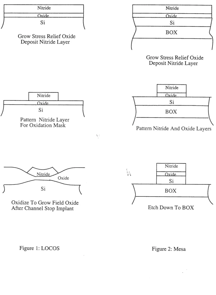
and non-LOCOS based. Local Oxidation Of Silicon (LOCOS) involves the selective oxidation of the silicon substrate around active device areas to grow a "field oxide" which dielectrically isolates discrete devices. Fabricating the isolation structure starts with the growing of a thermal, stress relief oxide (usually 20-60nm) and the deposition of a Chemical Vapor Deposition (CVD) nitride layer (usually 100-200nm). Next a photolithography step and subsequent nitride etch are used to define active areas. Once this is done, a channel stop implant and a final thermal oxidation (usually 300-1000nm) are performed to laterally isolate the defined active regions. The isolation structure is completed with the removal of the nitride layer[1]. Figure 1 shows the process sequence for conventional LOCOS. The lateral encroachment of the "Bird's beak, " which is inherent in LOCOS based isolation technologies, is proportional to the thickness of the field oxide grown. For this reason there have been a number of LOCOS based isolation schemes developed to reduce the Bird's beak encroachment while preserving the other needed isolation characteristics. The most well-known of the advanced LOCOS isolation technologies are Sealed Interface Local Oxidation (SILO) of silicon, Poly Buffered
LOCOS (PBL), and SideWAll Masked Isolation (SWAMI)[1,7,8]. Two isolation
schemes which developed from PBL are Framed Poly Buffered LOCOS and Sealed Poly Buffered LOCOS [9,10].
As the category implies, non-LOCOS isolation schemes involve achieving dielectric device separation through means other than selective oxidation of silicon. To date there are two sub categories of non-LOCOS isolation schemes, Selective Epitaxial Growth (SEG) and Trench/Refill[4,1 1]. SEG starts with a thermally grown oxide (usually 2iim). Next a trilayer resist coat and photolithography step are used to expose the areas where the "selective" growth will take place. After an anisotropic oxide etch to open windows to the substrate, polysilicon is deposited over the oxide while single crystal silicon, to be used for device fabrication, grows in the open windows. The isolation structure is completed with a step to planarize the wafer surface which removes the polysilicon from the top layer of isolation oxide[4]. Basic Trench/Refill begins with a stress relief oxide and a CVD nitride layer (both comparable to those thicknesses used in LOCOS). As in LOCOS, a photolithography step is used to pattern the nitride layer. Afterwhich the exposed nitride, oxide, and subsequently the silicon substrate are etched to form "trenches." A thin thermal oxide is grown and CVD oxide is deposited into the trenches to serve as the isolating dielectric. Completing the process is a Chemical Mechanical Polish (CMP) or Reactive Ion Etch (RIE) step to planarize the substrate
surface[11].
All of the above bulk CMOS isolation schemes have been proven effective for use in VLSI applications. Each has its attributes which makes it more attractive than others in specific cases. In general the particular isolation scheme chosen depends on the special concerns it has to address. Using conventional LOCOS as the baseline, complexity becomes an issue as more advanced LOCOS and non-LOCOS schemes attempt to reduce
lateral encroachment and in turn increase packing density, e.g., SEG and Trench have zero Bird's beak, but involve anisotropic etches, polysilicon deposition, and planarization techniques[7,8]. Good scalability is achieved by both non-LOCOS and advanced LOCOS schemes while planarity and latch-up immunity are dominated by non-LOCOS technologies due to the nature of the processes[4,11].
1.3 SOI Isolation Technologies
Silicon-On-Insulator (SOI) isolation differs from bulk isolation due to the buried dielectric, primarily silicon-dioxide (SiO2). Silicon-dioxide gives SOI technology intrinsic
vertical isolation; however, VLSI and future ULSI applications require total isolation. The two most prominent isolation techniques for SOI CMOS technology are conventional LOCOS and Mesa[12].
LOCOS isolation for SOI involves identical steps taken for bulk LOCOS; however, the field oxide grown for SOI is not as thick as that grown for bulk CMOS. The field oxide grown only has to be thick enough to oxidize the top layer silicon film thickness (tsi). Once the silicon film is oxidized down to the Buried OXide (BOX), the active device area is totally isolated from all others.
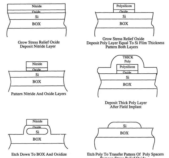
Mesa isolation begins similarly to LOCOS. First a stress relief oxide and a CVD nitride layer are grown and deposited, respectively. A photolithography step and nitride etch define the active areas where the mesas will be formed. After the nitride and oxide are anisotropically etched, the silicon substrate is RIE etched down to the buried oxide to form the mesa structure. The process is completed with the passivation of the mesa sidewalls which is usually done at the gate oxide step[12]. As in LOCOS for SOI, once
the isolation structure is fabricated, each active device area is totally isolated from any other. See figure 2. Oxidized Mesa and Rounded Edge Mesa are advanced versions of mesa isolation. Different from straight mesa, Oxidized Mesa utilizes a sidewall implant and an oxidation done directly after the substrate etch to round the corners of the mesa island. REM uses of the deposition, patterning, and anisotropic etching of polysilicon to form a mock (polysilicon) mesa structure with side spacers atop the substrate. An anisotropic etch transfers the rounded edge pattern to the substrate[12,13]. Figures 3 and 4 show the fabrication steps for Oxidized Mesa and REM, respectively. Both LOCOS and Mesa satisfy the needs for CMOS VLSI applications. Compared to bulk CMOS isolation SOI isolation is physically simpler; however, problems exist with each that raise concerns as to their effectiveness for use in the future ULSI era.
Lateral encroachment is a severe problem with LOCOS. Oxidation kinetics show that an oxide thickness of 2.2xtsi is needed to laterally isolate adjacent islands; however, it has been reported that due to stress build up in the silicon film, an oxidation time equal to triple that needed to grow an oxide 2.2xtsi thick on bulk is actually needed for isolation when field spacings are 1 am and below[1]. This poses a problem for realizing smaller devices when the film thickness is > 150nm due to severe lateral encroachment of the Bird's beak[1,14,15]. Oxide encroachment also presents a problem with parasitic transistors formed in parallel with the main device. If the width of this parasitic device is comparable to that of the main device, i.e., if lateral encroachment is extensive, the "subthreshold kink" will be manifested in the subthreshold slope of the device. Also a stress-induced, sharp-tipped Si filament located directly under the Bird's beak can be a
source of off-state leakage current. Moreover, if complete isolation is not achieved the filaments of adjacent active areas can touch, electrically connecting the islands[16,17].
Mesa-is plagued with gate oxide thinning and sidewall leakage. Due to the sidewall having a different crystalline orientation than the top of the mesa, the oxide thickness there can be 30% thinner than that on top. Gate oxide thinning is also present at the corners of mesa because of compressive-stress-limited diffusion. These two effects cause early gate oxide breakdown[12,14]. Parasitic sidewall devices are also inherent to mesa isolation as the gate of the devices stretches over the mesa sides. Charge sharing between the main and parasitic devices causes lowered threshold voltages at mesa corners. As in the case of LOCOS, this shows up in the subthreshold slopes of the device as leakage current. Oxidized mesa and REM offer advantages over straight Mesa by creating thicker sidewall oxides to prevent parasitics and rounding corners to reduce 2-dimensional charge sharing effects[12,13,14,].
In terms of the isolation characteristics needed for CMOS fabrication, LOCOS and Mesa are suitable for sub micron technologies; however, in making the transition from bulk to SOI, problems arise with device performance and leakage from parasitics. As is the case in bulk isolation, the determining factor as to which scheme is more applicable depends on the specific concerns the isolation scheme has to address for a given process.
1.4 Project Motivation
SOI technology has undergone much development over the last decade due to its potential use in VLSI CMOS applications. SOI offers many advantages compared to bulk technology, e.g., a simpler isolation structure and radiation-resistant circuits. Latch-up is
completely eliminated in SOI due to the absence of wells. The nature of Mesa isolation and the use of LOCOS with thin films guarantees higher packing density with SOI. Also in the case of thinner films, lowered junction capacitances and increased circuit speed will be achieved[l,14,18]. Although SOI substrates have the intrinsic vertical isolation and a simpler isolation process, isolation-related effects are manifested in device performance degradation. Thus the key issue of device isolation still must be addressed before SOI technology can enter into mainstream VLSI CMOS applications. Studying the effects of various process parameters, e.g., field-oxide thickness, field implants, and stress-relief oxide thickness on the different SOI isolation technologies will aid in understanding how each technology can be implemented in VLSI CMOS applications. Moreover, this will serve as the basis for investigating the potential of SOI technology for the upcoming ULSI era, where device geometries will be further scaled.
1.5 Organization of Thesis
Chapter two describes the design of the test structures used in the experiments and explains their purpose in the project.
Chapter three explains the design of the fabrication process, lists the process parameter splits, and explains how the process flow was generated.
Chapter four explains the simulation of the field-oxidations and the simulation tool used.
Chapter five explains the tests performed on the fabricated structures and devices. Data analysis and results obtained from testing will be given.
Grow Stress Relief Oxide Deposit Nitride Layer
Grow Stress Relief Oxide Deposit Nitride Layer
Pattern Nitride Layer For Oxidation Mask
Pattern Nitride And Oxide Layers
Nitride
Si
Oxide
,)
Si
Oxidize To Grow Field Oxide After Channel Stop Implant
BOX
Etch Down To BOX
Figure 1: LOCOS Nitride Oxide Nitride Si BOX Nitride Oxide
Nitride
C)Y;rlp Si BOX' ' ~`
""~
l Figure 2: MesaNitride
Oxide
Si
BOX
Grow Stress Relief Oxide Deposit Nitride Layer
Grow Stress Relief Oxide
Deposit Poly Layer Equal To Si Film Thickness Pattern Both Layers
Nitride
Oyxide.
Si
BOX
Pattern Nitride And Oxide Layers
Etch Down To BOX And Oxidize
Figure 3: Oxidized Mesa
'I
(
Deposit Thick Poly Layer After Field Implant
Si
BOXEtch Poly To Transfer Pattern Of Poly Spacers Remove Stress Relief Oxide
Figure 4: Rounded Edge Mesa (REM) Polysilicon
Si BOX
l Ir
Chapter II
Test Structures/Devices Design
2.1 Introduction
This chapter describes the design of the various test structures and devices used for the project. In addition to describing the basic design, a summary of variations in design parameters for each test structure and device are given. Finally, the purpose of each test structure or device in the experiment will be explained.
2.2 Isolation Islands
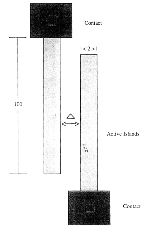
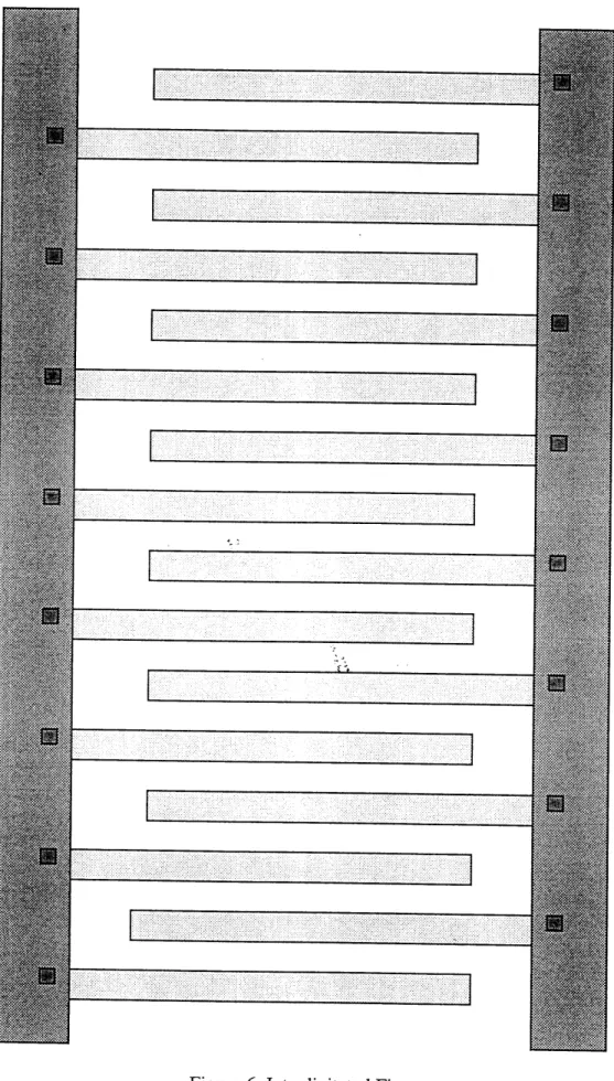
Figure 5 shows a layout of the basic isolation structure or "island" used to study the effects of process parameters on active area leakage current. It consists of two degenerately doped silicon strips (or fingers) separated by a field region dielectric. Focusing on 1-dimensional leakage, the aspect ratio of the structures was designed to decouple any 2-dimensional effects in leakage current in the structures. The length and width of the active structures were set to 100lm and 2jim, respectively. The features of interest in the structure were the "total active length" of the separated islands (100pm for the basic structure) and the separation or field spacing which, began at 0.4pm and varied up to 5pm. The variations in the structure were such that different total active lengths were obtained. See figure 6. In the case of figure 7, the aspect ratio was decreased to
introduce 2-dimensional effects in the leakage current. Table 1 summarizes the feature variations of the isolation islands.
Structure Basic Two Three Fingers Medium Sized Large Sized Parameters Fingers (2-D) Interdigitated Interdigitated
Active Width 2 2 2 2 (irn) Total Active Length 100 20 -20,000 -200,000 0.4, 0.5, 0.6, 0.4, 0.5, 0.6, 0.4, 0.5, 0.6, Field Spacing 0.7, 0.8, 0.9, 0.7, 0.8, 0.9, 0.5, 0.7, 1.0 0.7, 0.8, 0.9, (pm) 1.0, 1.2, 1.5, 1.0, 1.2, 1.5, 1.0, 1.2, 1.5, 2.0, 3.0, 5.0 2.0, 3.0, 5.0 2.0, 3.0, 5.0 Table 1.
The purpose of the isolation islands were to aid in the characterization of process parameter induced isolation effects. For LOCOS tlf parameiters were the isolation mask, field implant, and field-oxide thickness. The thermal stress relief oxide grown just prior to the deposition of the nitride layer serves as a buffer between the nitride layer and the silicon substrate. Although dependent upon temperature, the intrinsic stress of the as deposited nitride layer is on the order of 1010 dynes/cm2. Upon cooling, without a stress
relief oxide this nitride layer would impart a compressive stress on the order of 108 dynes/cm2 in the silicon substrate which would cause severe dislocation damage during a
subsequent oxidation[18]. The nitride/oxide layer thickness ratio determines the effectiveness of the buffering oxide layer. Generally, to alleviate the stress and prevent the
formation of dislocations, the minimum oxide thickness used should be 1/3xtnit, the thickness of the nitride layer[1].
The field oxide and field implant determines the physical completion and effectiveness of isolation by separating adjacent active areas and increasing the doping at the active area edge to prevent early inversion. Once the silicon surrounding an active area is oxidized down to the BOX, total isolation is achieved. Haond reported that the oxidation time needed to completely isolate active areas was much greater than bulk estimates. For isolation spacings on the order of lpm and below, it was found that the time needed for isolation was triple the time needed to grow an equivalent isolating oxide thickness on bulk. If the top layer silicon film is not completely oxidized in the field regions, silicon filaments would exist under the Bird's beak. Under oxidation would result in the electrical connection of adjacent active areas. For this reason, it was proposed that an extensive over oxidation be used to prevent the: Si filament, which can be a source of off-state leakage current in addition to intra-island leakage[12,14,15]. In his study of SOI oxidation kinetics, Crowder also reported the presence of Si filaments for sub micron field spacings. Crowder also noticed that over oxidizing silicon films resulted in the upward bending of the film due the expansion of the oxide grown at the back interface. This suggests that over oxidizing during the field isolation step may not be the best solution to the problem of active-area isolation by LOCOS technique. For example, as device dimensions and active area sizes further decrease, over oxidation conceivably may completely erase smaller active areas. Rather, optimization of the amount of field oxide
grown, and the field implant combination, should be used to achieve effective isolation[14].
The isolation structures were used to characterize SOI isolation through studying the effects process variation. Isolation process parameters were the isolation mask (nitride & oxide layers), field implant, and field-oxide thickness. By varying the field spacing and total active length parameters, the isolation structures were used to study process-condition-induced leakage effects, geometrical leakage effects, and packing density. The Mesa version of these test structures were used as controls in this experiment because once the mesa structure is formed, there was no conduction path between adjacent active areas, i.e., no leakage was expected.
2.3 Sidegating Structures
Figure 8 shows a section of the basic test structure used to study sidegating. It consists of active area strips (100ltm long and 2ipm wide) which are traversed by poly
silicon gates. The field region separating the active areas ranged from 0.5pm up to 2[tm. The layout of the gate lines and the alternating metal connections to the active areas were constructed to emulate the source and drains of MOSFETs. To effectively study sidegating, active area edges where the gate traverses a silicon step were needed. The actual structure used in the experiment consisted of 100 active areas and 10 gates lines giving a total of 200 edges where the gates crossed silicon steps. The width of the gate was set to 2pm. To give a control in this experiment, one structure consisted of an active area 100pm and 200ptm wide. The total area of this structure equaled that of the other
structures; however, the number of silicon steps for the gates to traverse was minimized. Table 2 summarizes the feature variations of the sidegating structures.
Structure Basic Control
Parameters Structure Structure
Active Area Width 2 200
(Am)
Active Area Length 100 100
(Pm)
Field Spacing 0.5, 0.6, 0.7, 0.8, 0.9, 1.0,
--(jim) 1.2, 1.5, 2.0
Table 2.
For LOCOS the resulting lateral encroachment from the Bird's beak creates a transition region between the field and active area regions. Coupled to the extent of the Bird's beak and the transition region is the amount of field oxide grown and the field spacing. As suggested above, the field oxidation time needed to completely isolate active areas was much longer than normal for submicron field spacings. This was due to the stress build up in the silicon film as the last remaining section of the film was being oxidized. Because the Bird's beak is proportional to the amount of field oxide grown, narrow field spacings and long oxidations would facilitate more lateral encroachment and thus a long transition between regions. It is desirable to have a short transition because a
long transition promotes sidegating, the formation of parasitics, and device performance degradation.
As mentioned in Chapter one, Mesa isolation inherently has parasitic devices due to the fact that the gate runs over the sidewalls of the structure and the tendency for the gate oxide to be 30% thinner on the sidewalls than that grown on the top. Also charge sharing between the main and sidewall device lowers the threshold voltage at the mesa corners. Sidegating in Mesa isolation results in the presence of sidewall leakage in the sub threshold current of devices[14]. Oxidized Mesa improves the quality of isolation by increasing the gate oxide thickness of the sidewalls and rounding the mesa corners if the oxidation is performed above 9650C, the viscous flow temperature of oxide[14].
Additionally, the sidewall implant increases the doping of the sidewalls thus increasing the threshold voltage of the sidewalls. Done effectively the presence of the sidewall leakage should not be a factor in the subthreshold slope of devices.
These test structures were designed to allow study of the dependence of field spacing, field oxidation, and field implant on sidegating for LOCOS. In the case of Oxidized Mesa the parameters were the sidewall implant and sidewall oxidation thickness.
2.4 Comb Diodes
Figure 9 represents the layout of the comb diode structures used in the experiment to study stress-induced diode leakage. Similar to a n-channel MOSFET from a top view, the structure has two n+ implanted regions separated by a polysilicon gate. The n+ regions are electrically connected to give the effect of a very large diode. Between the two abutted poly gate structures is a p+ region for contact to the substrate. The width of
the poly gate fingers and the active areas are each 2pm. There are a total of 100 gate fingers which gives a total of 200 intersecting points where leakage can occur. The length of the gate fingers and the length of the diode junction was set to 20pm for this device. There was one variation to the design of the device wherein the junction length of one structure was kept the same as above, while the number of intersection points was increased to 4000. Table 3 summarizes the design features of the comb diodes. Note: Due to the fact that this experiment was for NMOS technology, the diode structures designed will be fabricated, but will not be functional, i. e., no p+ implant was used.
Table 3.
As mentioned before, there is stress between the silicon nitride and the silicon substrate. The use of the stress relief oxide is to alleviate this stress and reduce the likelihood of dislocation defect formation; however, thin oxide layers allow more of the stress inherent in the nitride layer to couple into the substrate promoting the likelihood of substrate crystal damage. Dislocations extending across the n+/p junctions of the diode device would result in easier conduction paths for dopants causing unwanted leakage
Structure Diode 1 Diode 2
Parameters N+ Region Width 2 2 (t[m) Poly Gate/Junction Length 20 20 (Vm) " Number of 200 4000 Intersections
through the junction and possibly early junction breakdown [19]. In this experiment, the comb diodes were used to study the process dependent occurrence and effects of stress/damage induced leakage.
2.5
NMOS Transistors
The test structures mentioned in the above sections were designed to investigate discrete SOI isolation effects, namely active-area leakage, sidegating, and diode leakage; however, these effects are also manifested in the performance of devices. For example, in his study of the effects of sidegating on SOI transistors with LOCOS isolation, Chen found that the subthreshold current and subthreshold kink were dependent upon the width of the transistor. As previously mentioned, the kink in the subthreshold current was from a parasitic transistor in parallel with the main device. As the width of the main device is decreased, the subthreshold kink decreases due to the parasitic device characteristic over shadowing that of the main device. Also contrary,4o the Narrow Width Effect in bulk devices, as the channel width of a n-channel SOI MOSFET was reduced, the threshold voltage was found to decrease due to the overbearing presence of the parasitic device[16]. A host of transistors with W/L ratios varying from 50/50 to 1.5/0.15 were designed to allow investigation of the device performance and degradation under the influence of the above effects.
Contact
1<2>
< ->
Active Islands
Contact
Figure 5: Two Finger Isolation Structure 100
li
z
I
i
Contacts and Metal
:ts 1
->
k
2>
Contact and Metal to Source Regions
Active regions EI Poly gates E Metal
]ontact and Metal to )rain Regions
A IA ~op~o~rcaaar AA I A ~~II~~L A
j::~ ~
~oooEloo~araoa r A AI IIL IA A rr A dlRBIIBII~BBBB~$BBB~I~ * A A A ~·rm~o~p~rao~oaaa~ A A A "s~A I IL A I ~~LBIBBBB~~ A AA ~I~O~O~O~Q~ I A * A ~·p~eaaaa~~ A ~~~C~L~IIBI~I~I A A I ~IV0~1(4~0~~ A LL~OO~O~OI~P~D~*~ I IL ~~s~6sans~~ A A A ·1~6~6~6~6~ A A ~~~~sa~s868~1~L · h A ~II~BPP~L~P~PP~~~L I A A ~A~L~BBC * A ~A~l~ss1111166~8R~ A A A ~PIIP~P~PP~PP~P~C A IL A A ~Cdl~BBB~L88~8~B·r A A A A aaaaaaaa~aaaaa~ L· IL A ~~ci~aar~aa~~~ A L A ~QI~PIIP~O~C~L I A A A ~B~B~O A. A A ~~~O~a~o~op~~~ A A ~CC~P~~L~ A A A ~4~11~ A A A A ~~P~LL~L~L~L~II~ A A ~lh~Rsanea~a~-enr.~ A ~~LIIPPPPP~PL~~~L A A A ~I~LR A A ~~ ~116~18888~86618W~B AA A A A ~B~P~P~e~ A A I re ~C6·BBPI~IIIWIR~b~ A A r r ~PLII~PL~P~LR A A A A ~ss~ssaxm~nss~s~aa~ IL AIA ~Z~BBPBBBBPPBBBBO~~ I A ~A·ZD~P~L~P~O~BPP~ II A IL A ~L~L~BP~LI~L~J~PI A A A A A ~ I A ~~~~P~BBBPPPPPPPP~~ A A~~~~S~BIPBLI~BP,~ A ~~~CBPL~BP~P~III~~~ ~r~~F~WP~~~ ~~~·aa~applmp~eRwp~ AA A A A C~PL~II~L~B~ A A ~A~1~86~86666~6666~ AA A A Cc ~L~I~L~BO~d~8 A A ~~+rCI~P~B~I~I6~~~I AAA ~X·B~P~PPPI~BgPe~POIC I IL ~A~L~nrrr~pax~~L~ A A A ·e4i~6~dP~L~l~dl~R A A A A ~LE9P4~e~B~~~ ~~~·86~dWb6Q66~C+Q~ AA A A A~~P1Plb~gd~L~bi~~ A ~~~Q~PIP~L*I~ A A ~PPPBBPBBTB~PPP~PB Cc A ~r~L·Fl~b~W; * Cc AA ·L166~1~66~as6F~i~BBBB~L1 AcA A AA ·f3ee~L~BeBe~IdBp~ga888~~ · ·C· ~) rr~AL~Z~DJ~P~~* A r A ~h~841SB~BB~B~SBB~ r(I "" A~I~BP~I~$~IW~l~lssl~R AA AAA 8~6~P~C6~6B~P~I~~~ rc~~e~s~i~n~r~sc~w~ A AA Cc ~S~5~I~XPI~IILIG6db+I~h A A A A A·~PI~XL~L~PPL~LD# A A ~~~~B~IBr~65~~~ A A ~sr~n;mrrz~rp;spa r. A AAA BB~IWCIII~I~WIRR~R* A A IL ~~84~89~561~L~~~i AAA )5gQWe~i~Q~RIQLLI~ AA A IC A·IB~B6sBs680P~BTBB A A ~A~~I~L~B~P~YP~DJC~ A AA rrFSb~PBB61~L~BP~LB AA AAA · IL~Y~1&bb~CIBIB~PL I Ih AAI A L~~BBP~BPPPPPPBBBB~ ~·h1 AAA AIA AA ~IA1I AA A IL A ~i866b~5~6684~8~666~~ A A A A II In nrrn n L IL AIAAAAAAAA AAAIAAIAIIA IAAIAAAAAAH AIIAAAAAIAA AAAAAAAAAAI l~~~L1~1~~11~~1~~~~1~r AAAAAAAAAAAi AIIAAAAAAAAMetal and Contact Pad
Figure 9: Comb Diode
Poly
Chapter III
Fabrication of Test Structures
and Devices
3.1 Introduction
This chapter begins by describing the process parameter splits for both LOCOS and Oxidized Mesa isolation schemes. Next the tool used to originate the Process Flow Representation (PFR) will be discussed. Finally, the process flow will be explained. Generation of the process flow and device fabrication were done at the Microelectronics Laboratory (ML) at Lincoln Laboratory.
3.2 Process Parameter Splits
There were a total of sixteen Separation by IMplanted OXygen (SIMOX) wafers used in this experiment. Since LOCOS is the more prevalent isolation scheme and because it has more process variables, the focus of the experiment was skewed in its favor and more wafers were dedicated to its study. Twelve wafers were used for the study of LOCOS while the remaining four were used to study Oxidized Mesa. The goal of the parameter splits was to try to develop test structures and devices that had an overlapping mesh of parameters. While some parameters were common to both isolation schemes, each had its unique set of characterizing parameters.
There were two silicon-film thicknesses, tsi, used in the experiment. Due to the fact that the most interesting and promising uses for SOI lies in the use of thin films and
fully depleted devices, the first silicon-film thickness was set at 50nm[20]. The same motivation led to the second, yet more conservative film thickness of 90nm. Six LOCOS wafers had a -tsi of 90nm while the remaining six LOCOS and the four mesa wafers had a tsi of 50nm. The stress relief oxides used for the LOCOS wafers were 10nm and 35nm. With the masking nitride layer set to 100nm, the 35nm oxide was used to emulate a normal nitride/oxide ratio used for LOCOS while the 10nm oxide was used to intentionally introduce a stress factor into the experiment. Four of the LOCOS wafers of each film thickness had the 35nm oxide while two had the 10nm oxide. The influence of the stress relief oxide affected the Oxidized Mesa isolation only at the sidewall oxidation step. A 35nm oxide was used with all mesa wafers. There were a total of four different field oxidations used in LOCOS. As mentioned before, the study focused on the effectiveness of combining a "normal" field-oxidation time with field implants to achieve isolation. Starting with the wafers that had the 35nm stress relief oxide (for both film thicknesses), the field-oxidation times per wafer were chosen to give a 10%, 20%, 30,% and 40% over oxidation, with the normal oxidation time taken to be the theoretical time, as determined by TSUPREM-4, needed to oxidize down to the BOX. The four remaining wafers (two with 90nm tsi and 10nm oxide, two with 50nm tsi and 10nm oxide) received either a 20% and 30 % over oxidation. In order to ensure maximum possible control in the oxidations, the oxidation temperature was held constant for all oxidations while the oxidation time was varied. Each wafer received three Field implants. There were a total of 21 die per wafer. Four die to be used as controls received no Field implant, five die received field implant Fl, six die received field implant F2, and the remaining six die received field implant F3. Fl, F2, and F3 were 1E13, 5E13, and 1E14 BF2 implants for the LOCOS wafers, respectively. These implants, which were the sidewall implant for the Oxidized Mesa wafers, were 1E12, 5E12, and 1E13 BF2 implants respectively. The implant energy for wafer with tsi=90nm and tsi=50nm were 50Kev and 30Kev, respectively. The angle of the implants was set to 450, and each wafer was rotated 7200 while being implanted to
ensure that all sidewalls of the mesa received the implant. The sidewall oxidation thicknesses for the Oxidized Mesa wafers were set to 100nm and 200nm. These values were chosen to offset the removal of the sidewall oxide by subsequent etching of the stress relief and sacrificial gate oxides and to ensure proper rounding of the mesa corners as well as sidewall passivation. Tables 4 and 5 summarize the process parameter splits of each wafer for LOCOS and Oxidized Mesa, respectively.
Process Tnit Tsi SRO Field Field
Parameters/ (nm) (nm) (nm) Oxidation Implants
Wafer # (% over) 1 100 90 35 10 F1-F3 2 100 90 35 20 F1-F3 3 100 90 35 30 F1-F3 4 100 90 35 40 F1-F3 5 100 50 35 10 F1-F3 6 100 50 35 20 F1-F3 7 100 50 35 30 F1-F3 8 100 50 35 40 F1-F3 9 100 90 10 20 F1-F3 10 100 90 10 30 Fl-F3 11 100 50 10 20 Fl-F3 12 100 50 10 30 Fl-F3 Table 4.
Process Tnit Tsi SRO Field Sidewall
Parameters/ (nm) (nm) (nm) Implants Oxidation
Wafer # (nm) 13 100 50 35 F1-F3 100 14 100 50 35 F1-F3 100 15 100 50 35 F1-F3 200 16 100 50 35 F1-F3 200 Table 5.
3.3 CAFE
The process flow for the experiment was created by the Computer-Aided Fabrication Environment (CAFE) software system developed at MIT. CAFE was designed for use in all aspects of integrated circuit manufacturing, i.e., process design and planning and fabrication[21]. At Lincoln Laboratory CAFE is primarily used to generate the process flow for a wafer lot and as a tracking system for the lot as it is being processed. Process flows are generated by using, Flowtool, a program within the CAFE environment which manages a database of fabrication instructions or opsets. Flowtool operates by allowing the originator of the process flow to select and edit an opset corresponding to a particular fabrication step and write it to a Process Flow Representation (PFR) file. For example, selecting the "diff-ox-exp" opset from the opset database creates a window wherein all the parameters for an oxidation to be carried out by the diffusion bay can be entered. Figure 10 shows the results of selecting the diff-ox-exp opset, editing it, and writing it to a PFR file. This diffusion step was a step in the fabrication sequence of the experiment wherein wafers 1-8 and 13-16 receiv6e4 a dry oxidation at 10000C for 34 minutes with a 10 minute anneal in N2 at 10000C. As shown in the figure, the opset
window allows the originator to include any special instructions which maybe needed. Once the PFR file is completed, it can be loaded into the CAFE lot tracking system and wafer processing can begin. Once a fabrication step is carried out, CAFE advances the lot to a next queue for subsequent processing.
(diff-ox-exp :temp-C 1000 :dryox-time-min 34 :wetox-time-min 0 :anneal-temp-C 1000 :anneal-time-min 10 :anneal-gas ":N2" :rampdown-gas ":N2" :rampdown-temp-C 800 :expected-thickness-A 350 :number-of-points 49
:tagl " I got the settings from Bruce's logs----please confirm settings." :tag2 " Which furnace=? Might have to adjust time by a minute or so." :tag3 "These are SOI wafers...measure monitor for thickness." :wafsl ("1-8" "13-16")
:wafs2 ("1-8" "13-16") :wafs3 :none
Figure 10: 34 Minute Dry Oxidation Step
3.4 Process Flow
3.4.1 Wafer Thinning
The first step in the process flow was the thinning of the top layer silicon film. The starting top layer thickness and BOX thickness were 200nm and 380nm, respectively. Each of the SIMOX wafers used in the experiment were mapped using a SOI measuring program on a Prometrix 650FT Film-Thickness probe to determine the uniformity of the top layer film thickness. The average silicon-film thickness for a particular group of wafers was used for the thinning procedure calculations. In addition to the desired final silicon-film thickness, the starting film thickness included the amount of silicon consumed during processing. The fabrication steps that consumed silicon were the stress relief oxide oxidation, sacrificial gate and gate oxidations, and the S/D implant re-oxidation/activation. The actual thinning was done by growing a sufficiently thick oxide and removing it with Buffered hydrofluoric acid (BHF). For example, wafers 1-4 were wafers in the LOCOS splits which were to have a final film thickness of 90nm. The
thickness of the stress relief, sacrificial gate and gate oxides was 35nm, 5nm, and 5nm, respectively. All 16 wafers in the experiment received an activation re-oxidation that resulted in an oxide growth of 7.5nm. Taking the amount of silicon consumed by oxide growth to be 44% of the final oxide thickness, the wafers had to be thinned to approximately 113.6nm[19]. The average silicon-film thickness of this group of wafers was 204.4nm; therefore, a 201.7nm thick oxide was grown and stripped.
3.4.2 Device Process Flow
After each set of wafers were thinned to their respective starting thickness, the remaining process was that of an NMOS enhancement process for both types of isolation schemes. For the isolation mask (nitride/oxide), the wafers were dry oxidized at 10000
C
for either 4 or 34 minutes for grow the 10nm or 35nm stress relief oxide, respectively. This was followed by Low Pressure CVD (LPCVD) deposition of 100nm of silicon nitride. Advanced 248-nm lithography along with APEX-E photoresist was used to ensure the opportunity of studying close island spacings. After patterning the active device regions and plasma etching of the oxidation mask (the oxide was not removed with the LOCOS wafers), the mesa wafers were plasma etched in a LAM Autoetch 490 using CF4/He/C12 etch chemistry to form the mesa structure. Next each LOCOS wafer received the three field implants followed by its respective field oxidation while each mesa wafer received the three sidewall implants and its respective sidewall oxidation. All field oxidations were carried out at 10500C to coincide with the temperature used by Crowderin is study of SOI oxidation kinetics[15]. Also due to the fact that the field oxide thickness was a parameter and thin films were used, each oxidation run ramped the temperature in nitrogen only. This avoided any oxidation outside of the designated oxidation time. Figure 11 shows the numbering of the die for each implant. The shaded die are those which received the respective implant. The thermal cycle used to grow the
5nm sacrificial gate and gate oxides was an 800°C, 30 minute dry oxidation. The wafers with final a film thickness of 50nm and 90nm received VT adjust implant of 2.6E12 BF2 dose @ 30Kev and 3.3E12 BF2 dose @ 50Kev, respectively. The gate material was 250nm of amorphous silicon deposited at 570°C. After gate patterning, the source/drain implant consisted of a 5E15 arsenic dose @ 25Kev. Re-oxidation activation was performed on all wafers at 8500C for 30 minutes. The remaining process was standard
procedure for contact definition and metal deposition and patterning. The metal used for this experiment was a 600nm trilayer stack of TiN/AlSi/Ti. The thickness ratio for the trilayer stack is 100nm/450nm/50nm. Figure 12 shows a block diagram of the process. Figures 13 and 14 show pictures of the test structures at the completion of fabrication. Appendix A lists the PFR file generated with Flowtool.
eA
16
8 11 14 21 20 IVDie Numbering For Field Implants
Field Implant # 1 Field Implant # 2
Field Implant # 3
Figure 11: Die Labeling For Each Field Implant
I
ýffl"'~'2'''~''~''-`'~'''`'''''wdwmlmwodý ýN, 3 4 19 7 10 13 9 12 15 Mý~ IVField Oxide Growth Sidewall
Implant
,-D
S/D ImplantReox
4-Figure 12: Process Flow Diagram
Oxidized Mesa LOCOS
Three Finger Isolation Structure: 5.0Wpm spacing
Medium Sized Interdigitated Fingers Isolation Structure: 0.7pm and 1.Opm spacing
Sidegating Structure: 0.5pm Field Spacing Between Active Areas
Small Sized Comb Diode
Chapter IV
Simulation of LOCOS Field
Oxidations
4.1 Introduction
This chapter introduces the program used to simulate the LOCOS field oxidations for the experiment and explains the various options and parameters available for use in the simulation process.
4.2 TSUPREM-4
TSUPREM-4 is a computer program for simulating the processing steps used in the fabrication of integrated circuits and discrete devices. It is capable of modeling ion implantation, inert ambient drive-in, epitaxial growth, silicon and polysilicon oxidation, and low-temperature deposition and etching of various materials. The incorporation and redistribution of impurities is simulated in a two-dimensional cross section of the silicon wafer. Provided in the output of the program are the boundaries of the various material layers in the structure, the distribution of impurities in each layer, and the stresses produced by oxidation, thermal cycling, and film deposition[22]. For this experiment, focus was placed on those steps and parameters used to simulate the field oxidations of the LOCOS splits to determine appropriate oxidation times. Cross sections of the structure after oxidation were generated to determine the effectiveness of the oxidation, i.e., whether the silicon film was oxidized completely down to the BOX.
4.3 Simulation Procedure
The procedure for simulating field oxidations consisted of generating the input "stack" or file, which defines the initial silicon substrate and lists the fabrication steps to be simulated, and the actual TSUPREM-4 simulation of the input file. Initializing the substrate is done with TSUPREM-4 device-structure specification statements [22]. For bulk simulation the "mesh" statement along with the "grid.fact" parameter is the simplest method of defining the silicon substrate. This statement produces a rectangular, grided structure representing the wafer cross section. Due the fact that SOI wafers have two silicon regions separated by the BOX, the substrate/structure definition has to be done with the "line" and "region" statements. The line statement (used in both X and Y directions) defines the rectangular structure and sets the grid. The region statements define what material lies within a specified section of the structure[22]. Figure 15 shows the statements used to initialize the structure for the input file used to simulate those wafers with a top-layer silicon-film thickness of 90nm and the grid generated for the structure. The pitch of the grid is set with the "spacing" parameter. The top-layer silicon layer is located between y=Opm and y=O.11pm. The BOX is located between y=O.1l pm and y=0.5[nm, and the region below y=0.5pm is the handle wafer.
The fabrication processes modeled by TSUPREM-4 are approximated numerically using finite-difference and finite-element solution techniques. The solutions are calculated at the nodes of each triangle created by the grid; therefore, it is advantageous to have a denser grid in the top layer silicon film and at any "important" boundary consisting of two different materials as this gives more accurate simulation results. x=1.Opm is the center point of the nitride window where the field oxide is grown. The final step in defining the simulation structure was the initialization of the substrate background impurity concentration and the crystal orientation.
Figure 15 shows that the wafers used in the experiment had a background concentration of 1E15 Boron and a <100> crystal orientation. The remainder of the input
stack consists of the process steps to be carried out in the simulation program. Once the structure was defined, the isolation mask (stress relief oxide and nitride layers) was specified, and thermal oxidation was done using the "method" an "diffuse" statements. The method statement specifies the oxidation model the program will use, and the latter sets the diffusion parameters (time, temperature, oxidation type). The "deposition" statement along with its parameters, thickness and spaces, deposited the nitride layer of a specified thickness and set the grid for the layer. The nitride layer was etched in the field region with the "etch" statement, which selectively etched the specified material in particular sections of the structure[22]. Next the field oxide was grown by using the method and diffuse statements once more. Figure 16 shows the input stack that defines the structure to have a top layer silicon film thickness of 90nm, grows a 35nm stress relief oxide, deposits and selectively etched a 100nm nitride layer, and performs a 5 minute dry oxide at 1050TC. The resulting structure was used as the initial structures in the input stack that performed the field oxidation simulations for the wafers with various top silicon film and stress relief oxide thicknesses.
line x location=0 spacing=0.05 tag=left line x location=0.5 spacing=0.05 line x location= 1.0 spacing=0.01
line x location= 1.5 spacing-0.05 tag=right line y location=0 spacing 0.01
line y location--0.11 spacing-0.01 tag=boxtop line y location=0.50 spacing=0.05 tag=boxbottom line y location-1.0 spacing=0.1 tag=bulkbottom
region oxide xlo=left xhi=right ylo=boxtop yhi=boxbottom region silicon xlo=left xhi=right ylo=boxbottom yhi=bulkbottom init boron=lel5 <100> -~ .,,,.~.., I ,,,,, I /
/
/I
7-I I I
7,
/ / / / / / ,i -, .. v vxvvjrrrr j r: V V , // 0.80 Distance (microns)Figure 15: Statements Used To Generate Grid And Grid
2
/
2 7 7/
///
///
I I i/ 2 7 7 7/
/
7
/
7
7
7 7 //
/
/
7
/
2 1• / 2 77
/7
7
7
7
c-u CU Iz COMV/h/
-/0cD/
0.00 z //
2 7i
/*
/
z
/ z ,/7
7
7
7
7
7
7
//
/
7
7
//
7
/1
7/
I I /7,
7,
7 7/
/,/
/~7
/1
7 7 7i 7i 71 7 2 //
/
/
//
/1
7-/ / /7
7
7
7
7
7
0.40 1.20L
I
ý11
/~EF~IEE~F~
A A A A A • • vrrrryrr••/
rvvV r€, / /r ./VVVVVf VVVV////t/N///UM
!//!1M-/11
///MA•
/i/
iiI//F1//1
zz z/ /Zv/Z
,,,-F
$ Setup SOI substrate, initialize grid
line x location=0 spacing=0.05 tag=left line x location=0.5 spacing=0.05 line x location=l.0 spacing=0.01
line x location=1.5 spacing=0.05 tag=right line y location=0 spacing 0.01
line y location=0.11 spacing=0.01 tag=boxtop line y location=0.50 spacing=0.05 tag=boxbottom line y location-1.0 spacing=0.1 tag=bulkbottom
region oxide xlo=left xhi=right ylo=boxtop yhi=boxbottom region silicon xlo=left xhi=right ylo=boxbottom yhi=bulkbottom init boron=1el5 <100>
$ Grow Stress relief oxide----350A
method vertical dy. oxide=0 grid.oxi=4 init=0.15 diffuse temp=1000 time=4 dryo2
$ Deposit nitride layer----1000A deposition nitride thick=.1 spaces=2 etch nitride right pl.x=0.8
$ Use compress model to perform 5min dry oxidation method compress grd.oxi=4 init=0.15
diffuse temp=1050 time=5 dryo2 structure outfile=simox900-350.5dryc stop
Figure 16: Model TSUPREM-4 Input Stack
4.4 TSUPREM-4 Oxidation Models
4.4.1 Oxidation Theory
Oxidation in TSUPREM-4 is based on the theory of Deal and Grove[22]. The flux of oxidant (either 02 or H20) from the bulk of gas of the oxide/gas interface is given by
F=h(C*-Co)
(4.4.1)
where h is the gas-phase mass-transfer coefficient, Co is the concentration of oxidant at
the oxide surface, C*= Hpg, H is Henry's Law constant and pg is the partial pressure in the oxidant in the bulk gas. The flux of oxidant in the oxide is
F=D(Co-Ci)/y
where d is the diffusivity of the oxidant in the oxide, Ci is the concentration if the oxidant
at the oxide-silicon interface, and y is the thickness of the oxide. The rate of the oxidizing interface is
F=ksCi (4.4.3)
where ks is the chemical surface-reaction rate constant for the oxidation. Solving the
equations gives
N(dy/dt)=F= ksC*/(1 + ks/h + ksy/D) (4.4.4)
where dy/dt is the oxide growth rate and N is the number oxidant molecules per cubic centimeter available for the oxidation. Equations (4.4.1)-(4.4.4) solved one dimensionally, gives
y2+Ay-B(t-t)=0 =O (4.4.5)
where A-2D (1/ks + 1/h), B=2DC*/N, and t - (yo2 + Ayo)/B. yo is the amount of oxide
grown prior to oxidation. A and B are expressed in terms of the linear and parabolic rate constants B/A and B, respectively[22,23].
TSUPREM-4 uses both analytical and numerical oxidation models. The analytical models, ERF1, ERF2, and ERFC models, are designed for very fast and rough simulation of basic structures. These models are limited to structures which are planar and may be covered by an oxide layer. When using these oxidation models, all oxidation masking layers present on the initial structure are ignored. Due to the topography of the wafer surface after nitride patterning, the analytical models are insufficient for simulating (4.4.2)
LOCOS field oxide growth. The numerical oxidation models, VERTICAL, COMPRESS, and VISCOUS are designed to accurately simulate any structure, regardless of the surface topography or oxidation masking layers. Using equations (4.4.1)-(4.4.4), these models calculate the oxide growth rate at every point of the oxide/silicon interface[22]. The difference in the numerical models lies in the method in which the oxide flow caused by volume expansion is calculated. The VERTICAL model, the least complex and least accurate of the three, was used to simulate the growth of the stress relief oxide due its speed and the planarity of the structure surface at the time of this processing step. The COMPRESS model, the second simplest, and the VISCOUS model, the most complex and most accurate, was used in the simulation of the field oxidation where the structure topography was not planar due to the presence of the nitride oxidation mask.
4.4.2 COMPRESS Model
The COMPRESS model simulates the viscous oxide flow during oxidation. The movement of the oxide-silicon interface across the structure is two dimensional, and the variation of the crystal orientation is accounted for when the oxidation rate is calculated. The model uses the finite-element solutions approach (with three nodes per triangle) to offer speed in the calculations. Defining a very dense grid when using this model increases the simulation time, as there are more triangles present in the structure; however, more accurate results are obtained. In order for the model to remain numerically well-behaved, a small amount of compressibility is allowed. Due to this, as well as the simple approach to performing calculations, the COMPRESS model cannot be used to calculate accurate values of stress[22].
The COMPRESS model was used to determine the approximate oxidation times needed for the experiment. Once the time it took for the field oxide to just reach the BOX was determined, the percent over oxidation was calculated and simulated to generate the
cross sectional profiles for the structures. Figure 17 shows the input stack used to grow the field oxide using the COMPRESS model. The time listed in the input stack is that needed for the 10% over oxidation for wafer 1. The "initialize" statement with the in.file parameter specifies the structure with a structure file generated with the input stack in figure 16. The method statement was used as before to determine the model to be used in the oxidation. Once the oxidation was performed, the output structure was then saved for future reference and cross section generation.
$ Initialize structure with presaved structure initialize in.file=simox900-350.5dryc
$ Choose oxidation model and perform oxidation method compress grid.oxi=4 init=0.15
diffuse temp=1050 time=18 weto2 $ Save output structure
structure outfile=simox900-350.18c
Figure 17: COMPRESS Model Input File
Figure 18 shows a graph of remaining top layer silicon versus oxidation time for each of the top layer silicon/stress relief oxide thickiiksses combinations, i.e., 90nm/35nm, 90nm/10nm, 50nm/35nm, and 50nm/10nm. This graph accurately shows that the COMPRESS model does not account for stress in its calculations. This is evident from the linearity of the plots. The curves would become more parabolic as the oxidation increased due the stress that develops in SOI substrates as the last section of top layer silicon is oxidized. Figures 19 through 22 show the sections for wafers 1-4, respectively. The width of the nitride window is 0.4pm for all structures.
100 80 60 40 20 0 0 5 10 15 20 Time (min)
0.00 0.50 1.00 1.50
Distance (microns)
Figure 19: Cross Section For Wafer 1, (10% Over Oxidation, COMPRESS Model)
ccC 0 L u E a( u C-C D oCS Cr 2.00
0.00 0.50 1.00 1.50 Distance (microns)
Figure 20: Cross Section For Wafer 2, (20% Over Oxidation, COMPRESS Model)
Cl) C 0 L u a) C) C n o C! Cl 2.00
C 0 C-_ c-) E 0 L C-D CD) SinI,,- ' Distance (microns)
I 6') L C-O E 0 C CDi CV) Distance (microns)
Figure 22: Cross Section For Wafer 4, (40% Over Oxidation, COMPRESS Model)