I
A Distributed Data Acquisition Network for
Vibration Measurement
by
Jeremy Thomas Braun
Submitted to the Department of Electrical Engineering and Computer
Science
in partial fulfillment of the requirements for the degree of
Master of Engineering in Electrical Engineering
at the
MASSACHUSETTS INSTITUTE OF TECHNOLOGY
May 2003
@
Jeremy Thomas Braun, MMIII. All rights reserved.
The author hereby grants to MIT permission to reproduce and
distribute publicly paper and electronic copies of this thesis and to
grant others the right to do so.
Author.
uYepartment
of Electrical Engineering and Computer Science
May 19, 2003
Certified by...
J. Kim Vandiver
Professor of Ocean Engineering
T 4esis Supervisor
Accepted by... ...
Arthur C. Smith
Chairman, Department Committee on Graduate Students
MASSACHUSETTS INSTITUTE OF TECHNOLOGY
JUL 3 0 2003
A Distributed Data Acquisition Network for Vibration
Measurement
by
Jeremy Thomas Braun
Submitted to the Department of Electrical Engineering and Computer Science on May 19, 2003, in partial fulfillment of the
requirements for the degree of
Master of Engineering in Electrical Engineering
Abstract
Current data acquisition technology for studying vortex-induced vibration (VIV) in underwater pipes is insufficient for studying mode shape and high mode number vi-brations. This work presents a prototype data acquisition system capable of acquiring high mode number data suitable for mode shape analysis. A suitable VIV experimen-tal setup is presented, and the instrumentation design hurdles are analyzed. Using modern surface mount technology electronics, a prototype printed circuit board was designed and built. The prototype node is capable of being networked with other devices on an RS-485 serial bus to provide many simultaneous data capture points along the length of a pipe. Bi-axial acceleration data are sampled using a sigma-delta analog to digital converter, and stored in a local EEPROM by a PIC microcontroller.
A networked serial communications protocol is developed, and the software for both
the node microcontroller and a host computer that controls the sampling process is described. Sampling parameters and firmware updates can be carried out remotely over the serial bus, and captured data can be uploaded back to the host computer at the surface. The prototype's analog and communications performance is analyzed for robustness and scalability. Recommendations for future work to improve the performance of the device are given.
Thesis Supervisor: J. Kim Vandiver Title: Professor of Ocean Engineering
Acknowledgments
Many people have helped me through my time at MIT. First and foremost, my parents put me through my first four years of school and always have offered their support freely. Kim Vandiver, John Kassakian, Jeffrey Lang, Paul Gray, Ron Roscoe and Kent Lundberg all had an enormous impact on my academic life throughout college.
My roomates Rita and Emily deserve thanks for putting up with me while I wrote
my thesis, and for valuable proof reading comments. Sherri, for being a friend and companion. Anne Hunter, for being available and clueful at all hours of the day. The theater staff at Rinaldi Tile Company for teaching me to sew, build and relax. TE41 Xi chapter for many fond memories and a rich undergraduate life. Rachel, for always having a shoulder free.
Contents
1 Introduction 13
2 Background and Motivation 15
2.1 Vortex Induced Vibration . . . . 15
2.2 Limitations of Current VIV Data . . . . 16
3 Proposed Experiment 19 3.1 Physical System Requirements . . . . 20
3.2 Accelerometer and ADC . . . . 22
3.3 Communications Bus . . . . 23 3.4 D ata Storage . . . . 23 3.5 C ontrol . . . . 23 4 System Implementation 25 4.1 Accelerometer Node . . . . 25 4.1.1 Accelerom eter . . . . 26
4.1.2 Buffer and Filter . . . . 26
4.1.3 Analog to Digital Converters and Coupling Network . . . . . 28
4.1.4 M icrocontroller . . . . 30
4.1.5 External Data EEPROM . . . . 31
4.1.6 RS-485 Serial Bus Transceiver . . . . 31
4.2 Serial Communication Protocol . . . . 31
4.3 Node Firmware . . . . 34
4.3.1 Bootloader . . . . 34
4.3.2 User Firmware . . . . 36
4.4 Host Computer Software . . . . 39
4.5 Sampling Process Overview . . . . 40
5 Results 45 5.1 Printed Circuit Board . . . . 45
5.1.1 Layout Considerations . . . . 46 5.2 Software Test . . . . 47 6 Future Work 49 6.1 Data Transmission . . . . 49 6.2 A liasing . . . . 51 6.2.1 Filter Types . . . . 51 6.2.2 Filter Implementation . . . . 56
6.3 ADC Selection and Analog Front End . . . . 57
6.4 Board Size and Layout . . . . 57
7 Conclusions 59 A Sallen-Key Circuit Analysis 61 B Prototype PCB CAD Drawings 63 C Bessel Filter Design 67 C.1 sallenkey.m . . . . 67
C .2 besselvalues.m . . . . 68
C.3 Implementation . . . . 68 D PIC Bootloader Assembly Code 71 E PIC User Firmware Assembly Code 83
List of Figures
2-1 A cylinder shedding vortices
3-1 Cut-away view of a section of pipe . . . .
3-2 Accelerometer node in a coiled section of
4-1 System block diagram . . . .
4-2 Acceleration signal path detail . . . .
4-3 Low pass filter frequency response . . . .
4-4 Typical switched capacitor input . . . .
4-5 ADC input coupling network . . . .
4-6 Packet contents . . . . 4-7 Autobaud timing diagram . . . .
4-8 Experiment setup window . . . . 4-9 Flowchart of the sampling process . . . . 4-10 Sample cookie node selection dialog . . .
4-11 Default experiment configuration dialog .
5-1 Prototype printed circuit board . . . . .
5-2 Accelerometer mounting . . . .
5-3 Captured test traces . . . .
6-1 Dual serial bus implementation . . . . . 6-2
6-3
6-4
Sample 5 Vpp square wave captures demo Sample anti-aliasing filter frequency respo
Filter transient responses to a 10 Hz squa
. . . . . 19 pipe . . . . 20 . . . . 25 . . . . 26 . . . . 27 . . . . 29 . . . . 30 . . . . 32 . . . . 33 . . . . 40 . . . . 42 . . . . 43 . . . . 44 . . . . 45 . . . . 46 . . . . 47 . . . . 50 nstrating aliasing . . . . 52 nses . . . . 54 re w ave . . . . 55 . . . 15
A-i Generalized Sallen-Key op-amp circuit . .
Prototype schematic . . . . Top copper layer . . . . Ground copper layer . . . .
Vcc copper layer . . . .
Bottom copper layer . . . .
C-i Schematic: 12th order Bessel low-pass filter C-2 Prototype 12th order Bessel low-pass filter
B-i B-2 B-3 B-4 B-5 . . . . 6 4 . . . . 6 5 . . . . 6 5 . . . . 6 5 . . . . 6 5 69 69 . . . 61
List of Tables
4.1 LTC2440 oversampling ratios and data output rates . . . . 29
4.2 Serial control characters . . . . 32
4.3 Serial command definitions . . . . 43
Chapter 1
Introduction
Modern offshore oil and gas production requires floating drilling and processing facil-ities in water depths exceeding 5000 feet in the Gulf of Mexico. Exploration drilling and oil and gas production require long cylindrical drilling risers and production tub-ing and pipelines. These cylinders reach 55 inches in diameter for vertical drilltub-ing risers and 28 inches for catenary production risers. They are most often made of steel. In the case of catenary risers they may exceed 8000 feet in length. Ocean currents can cause these large steel cylinders to experience vortex-induced vibration (VIV). Vortices shed off the pipes as water flows past them. Lift and drag forces from the vortices cause the pipes to vibrate, which may result in fatigue of the steel and possible failure.
Low mode number vibration has been studied on short pipe lengths in controlled laboratory environments. Experiments with longer pipes have been conducted in limited numbers under uniform flow conditions. Real offshore risers experience non-uniform, or sheared, currents in the ocean. These currents can excite multiple modes and higher mode numbers in long sections of pipe. Few high quality data sets are available that permit the evaluation of high mode number vibration and mode shape identification. Data samples must be taken at many locations simultaneously along the length of the pipe which is not feasible in a long pipe using current instrumentation schemes.
nea-surement at a large number of locations for a reasonable cost. The system will enable response amplitude and frequency analysis over the entire riser length. The design solves many deficiencies of currently available instrumentation schemes.
Chapter 2
Background and Motivation
Some background information about VIV is necessary to understand some of the requirements and challenges present in the design of this data acquisition system. The limitations and shortcomings of current data collection methods are also discussed.
2.1
Vortex Induced Vibration
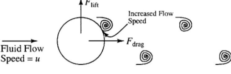
A cylindrical body positioned perpendicular to a fluid flow will shed vortices in its
wake. For a particular cylindrical body in a flow, the Reynolds number is defined as Re =!2 where D is the diameter of the pipe, u is the flow velocity, and v is the kinematic viscosity of the fluid. As the Reynolds number becomes larger than about
100, vortices shed from alternate sides of the cylinder, as shown in Figure 2-1.
Fi~ft
Increased Flow Speed
Fluid Flow drag
Speed = u
Figure 2-1: A cylinder shedding vortices
Increased local flow speed where the vortex is formed leads to reduced pressure, which applies a lift force transverse to the flow to the cylinder. When a vortex is shed from the opposite side of the pipe a force is experienced in the opposite direction.
The frequency at which this shedding occurs is called the Strouhal frequency, and can be found as
_ SeU SD
The constant st is the Strouhal number (experimentally found to be ~ 0.17 for flexible moving cylinders). Each vortex also has a drag component associated with it inline with the flow direction. This force is applied with each vortex so it occurs at twice the Strouhal frequency. The lift and drag forces are both proportional to the square of the flow speed.
If
f,
is close to a natural frequency of the pipe the vortices will positively reinforce its vibration. This is a behavior called lock-in, and typically exhibits vibrations with the largest amplitude, and most strain.When the Strouhal frequency and the pipe's natural frequencies do not coincide the behavior of the pipe is hard to predict. Several different modes can be excited in the pipe, and the amplitude fluctuates drastically. In some cases the higher frequency inline vibrations, caused by the drag force of every vortex, can dominate the pipe's response if they occur near a natural mode of the pipe. When the fluid flow is sheared (varies with depth) multiple vibrational modes of the pipe can be excited at the same time.
2.2
Limitations of Current VIV Data
The mode shape of long pipes experiencing high mode number VIV is of immediate interest in this research area. There is a paucity of data that is of sufficient spatial density to analyze this type of behavior. In order to look at mode shapes, the acceler-ation of the vibrating pipe must be sampled at many locacceler-ations simultaneously along the length of the pipe. VIV acceleration data are not always collected in a manner which allows easy mode-shape analysis.
There are two main sources for VIV data: smaller laboratory research experi-ments and real data from offshore risers. Laboratory experiexperi-ments often have many accelerometers wired back to a central data collection computer, which does collect
data samples simultaneously along the length of the pipe. Since these experiments are usually conducted in a laboratory setting, they are often on too small a scale to excite higher mode numbers in the test pipes.
Data collection on offshore risers presents some other interesting challenges. It is prohibitively expensive to wire a significant portion of the riser with accelerome-ters each of which is connected directly back to the surface. Large portions of the risers can be instrumented using small, autonomous battery-powered units which are attached to the riser as it is deployed and collected weeks or months later. Unfortu-nately, because each node's sampling clock is free-running, the samples are all taken at different times with respect to one another. Thus the data are often useless for mode-shape analysis.
Clearly another instrumentation solution is needed. This paper details the design of a data acquisition system that would be suitable for acquiring the synchronous
data sets needed to study high mode number VIV.
Fairing research is another area where this system would be useful. The industry standard way to prevent VIV is to add pivoting fairings to the risers, which prevent the formation of vortices in ocean currents. Few data are available on how long sections of pipe perform with different fairing coverage patterns. A suitably instrumented pipe could be used to determine whether 25%, 50%, or 100% of the pipe's surface requires fairings to effectively suppress VIV.
Chapter 3
Proposed Experiment
In order to study high-mode-number VIV, a very long (relative to its diameter) pipe is required. The proposed experimental apparatus consists of a 400 foot length of fiber reinforced composite tubing with a 1" inner diameter, and 1.38" outer diameter. Inside the pipe will be a number of nodes, each equipped with a bi-axial accelerometer with its sensitive axes perpendicular to the axis of the pipe. Figure 3-1 contains a
Instrumented Pipe Cross Section
Approximately 400 ft long 1" ID fiber reinforced epoxy
pipe filled with urethane Molded top end connector
Approximately 50 networked bi-axial accelerometer nodes
Additional instrumentation nodes possible (bi-axial inclinometer shown)
Figure 3-1: Cut-away view of a section of pipe
'41;
conceptual cut-away view of a section of the pipe. Each individual node will contain analog-to-digital converters for each accelerometer axis to digitize the acceleration data, and a storage element to hold that data. All of the nodes will be linked together on a communications bus, so they can be controlled remotely from the surface, and so that the experimental data can be transmitted back to the surface.
The number of required nodes is driven by a spatial Nyquist criterion. Mode shapes are approximately sinusoidal. At least two measurement points per wavelength are required. For the planned experiments the mode number may be as high as 30. The number of wavelengths is n/2, so the required minimum number of sensors is approximately 30. The number of required sensors increases in proportion to peak flow velocity.
3.1
Physical System Requirements
The biggest design challenge is making the printed circuit board (PCB) small enough to fit inside the pipe. In order to store and transport the pipe, it must be coiled into a spool about eight - ten feet in diameter. Therefore, the board must be made narrower to keep it from binding inside the coiled pipe and breaking. Figure 3-2 shows a diagram of a coiled section of pipe containing an accelerometer node. From
I i
Figure 3-2: Accelerometer node in a coiled section of pipe the diagram, the required width of the board in inches can be found as
A a six inch long board would require a width of not more than .91".
Another physical restriction on the design of the PCB is that components which stand a significant distance off of the board can not be used, as they will not clear the wall of the pipe - especially near the edges of the board. For these reasons, surface mount technology (SMT) components should be used wherever possible as they save
50% or more of the space of normal through-hole components.
To insert the nodes into the final 400 foot long pipe, they will have to be pulled along on a string or other strength member. It is a poor idea to use the communica-tions or power wires for this as it is too easy to break a solder connection, and render the entire system unusable. One way to prevent this is to run a long kevlar string along the underside of all the boards. Each board is anchored to the string, leaving some slack in the connecting wires to protect them from damage. When laying out the circuit board, space must be left for this strength member to run so that it does not rub against any components and damage them.
Once inside the pipe, the nodes have to be physically coupled to the pipe to accurately measure its acceleration. If they are left free, the circuit boards will rattle inside of the pipe, corrupting the quality of the data. The usual solution to this problem is to fill the pipe with a potting compound upon final assembly. Potting compounds in general are liquid mixes which can be poured into hollow spaces and which harden later. Care must be taken to select a potting material that is not too stiff, as using too hard a potting compound may cause the solder joints or PCB traces to break when the pipe is vibrating. The potting compound must have enough give to prevent it from ripping components from the board during operation and storage. It must also be non-conductive to prevent it from causing electrical shorts on the boards.
Filling the pipe with potting compound is an irreversible procedure. Once the compound hardens, physical access to the nodes is no longer possible, short of cutting the pipe open. Therefore, during the design process it is important to keep in mind that the device should be electronically configurable from the surface through the communications bus.
3.2
Accelerometer and ADC
Once the nodes are potted inside of the pipe, the orientation of the accelerometer's sensitive axes needs to be determined relative to each other. The easiest way to do this is to place the pipe flat on the ground and roll it over slowly while collecting data. The earth's ig gravitational field will register on a DC-sensitive accelerometer and the orientation of each accelerometer can be determined from these data. Accurate
DC sensitivity will heavily influence the design choices made in the analog signal path
in section 4.
The fundamental frequencies of interest range up to about 25 Hz. Ideally the third harmonic would be preserved as much as possible as this is often a significant com-ponent of vortex-induced vibration. The Nyquist Theorem requires that a sampling rate of at least 150 Hz be used. Since building a perfect low-pass filter is impossible, increasing the target sample rate to 250 Hz gives about an octave in which to design an appropriate anti-aliasing filter.
As discussed in section 2.2, every ADC needs to sample at the same time in order to study mode shapes of the pipe. Therefore, the converter chosen should be externally triggerable. In addition, some method of distributing a triggering signal to all of the ADCs in the pipe needs to be developed.
Other considerations include ADC resolution and accelerometer range. In order to provide the needed dynamic range for slower speed (lower amplitude) experiments, an ADC with at least 16 bits of resolution is desired. Recall from section 2.1 that the forces exerted by the vortices are proportional to the square of the flow speed. For the faster planned experiments the peak acceleration experienced will be on the order of 20g - 30g. The chosen accelerometers must be able to measure signals of this
magnitude. A programmable gain element in the analog signal path could also be useful in increasing the dynamic range for lower-amplitude signals.
3.3
Communications Bus
A serial communication bus is the ideal choice for data transfer in this system. The
number of wires that can fit inside the pipe is small, so the less wires, the better. RS-485 is an asynchronous serial communications protocol which allows for speeds up to 10 Mbps, and up to several hundred nodes to be connected together on a shared bus up to 4000 feet in length. The data signal is transmitted along a pair of differentially-driven wires, which provides high noise immunity and good data retention over long distances. RS-485 transceivers are available in tiny packages from several manufacturers, and inexpensive 100 Q unshielded twisted pair (UTP) Ethernet cable is perfect for wiring the bus.
3.4
Data Storage
To extract useful information from an experiment's data set, at least 20 cycles of steady-state VIV need to be monitored. With two 16-bit channels sampling a 1.0 Hz signal at 250 Hz the storage required for each node is
32 bits .2 5 0 samples .20 cycles = 160 kbits
sample sec 1 Hz
A few EEPROM products are available in small SMT packages with this capacity,
and many FLASH products are available in much larger capacities, if desired. The prototype uses 512 kbit 24LC515 EEPROM from Microchip. It provides plenty of storage space and is available at reasonable costs from Digikey and other distributors.
3.5
Control
Each node needs to have a microcontroller or microprocessor to control the syn-chronous sampling procedure, data storage and retrieval, serial communications, etc. The chosen microcontroller should be small, easy to program, and should have periph-eral units that facilitate these functions. Because physical access to the nodes will be
impossible once installed in the pipe, it is extremely useful to chose a microcontroller with the ability to re-program itself remotely from the surface.
Chapter 4
System Implementation
The first part of this section discusses the actual node hardware components. The second section details the serial communication protocol used. The third and fourth sections discuss the software for the individual nodes, and the host computer, respec-tively.
4.1
Accelerometer Node
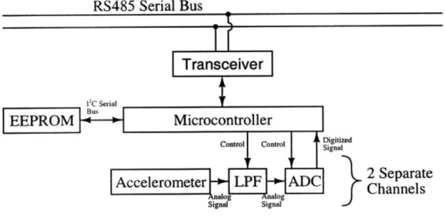
A system block diagram is shown in Figure 4-1. A detail of the acceleration signal
RS485 Serial Bus
Transceiver
1zC Ser
EEPROM ...Microcontroller
Control Control 'igntize
Signal 2r Sepr't
Accelerometer LPF ADC 2 Sepate
alg 0 Channels
Figure 4-1: System block diagram
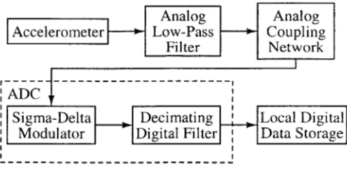
path is shown in Figure 4-2. The acceleration signals from the accelerometers pass through some buffering op-amps, a low pass filter, and a compensation network into the analog to digital converters (ADCs). A microcontroller interfaces with the
Analog Analog
AccelerometerT--+ Low-Pass -+Coupling Filter Network
|ADC 1
Sigma-Delta Decimating Local Digital Modulator Digital Filter Data Storage
Figure 4-2: Acceleration signal path detail
ADCs, triggering each sample and retrieving the last conversion performed. The
microcontroller stores the data in an external EEPROM and provides various services over the RS-485 bus, described in sections 4.3.1 and 4.3.2.
4.1.1
Accelerometer
The accelerometer chosen for the prototype node is the ADXL250 from Analog De-vices. The ADXL250 contains two micro-electromechanical (MEM) accelerometers, oriented orthogonal to each other in the plane of the chip. It comes in a 14-lead
surface mount cerpac package, small enough to fit inside of the composite pipe. Both channels are capable of producing a ±50g signal, at 38 mV/g.
Both channel outputs are differential signals referred to a reference voltage gen-erated on-chip which is nominally one half the power supply voltage. The reference voltages for the x and y channels are available at the x0ff and yoff terminals of the
ADXL250 respectively. It also offers decent noise performance of about lmg/v/Hz, and can operate from a single 5 V supply.
4.1.2
Buffer and Filter
The output resistance of the accelerometer reference channel is 30 kQ, and the output amplifier of the device is capable of supplying up to 100jA. In order to drive the ADCs, these signals must be buffered by a unity-gain op-amp. In addition, the
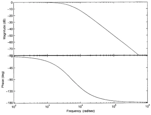
accelerometer signals need to be low-pass filtered to avoid aliasing problems. The LTC2440s sample at 1.8 MHz. The low-pass filter consists of a second-order low-pass
filter implemented with a Sallen-Key circuit. See appendix A for a treatment of the Sallen-Key architecture. The 3 dB point is located at 880 Hz. The 40 dB/decade rolloff provided by the low pass filter provides 120 dB of attenuation at half the sampling frequency (900 kHz). The phase shift of the filter is about -4' at 25 Hz, the highest principle frequency of interest, and the magnitude is only attenuated by
7 mdB. The frequency response of the low-pass filter can be found in figure 4-3.
0 -10- -20-R -30 --40 0) 50 -60 -- -70--8@ -45-D-90 ---135 -180-102 3 104 105 10 Frequency (rad/sec)
Figure 4-3: Low pass filter frequency response
Accurate DC performance is also a requirement of the sampling system. Most op-amps have a small (several mV) DC offset voltage associated with them. At sen-sitivities of 38 mV/g, several offset voltages added together will become a significant source of error at low amplitudes of experienced acceleration. In order to preserve performance with little DC offset error, expensive chopper-stabilized op-amps can be used. The LTC2052 was selected for its low noise, rail-to-rail output capability, and single 5 V supply operation. The op-amps periodically disconnect the op-amp (internally) from the input and output pins, and measures the offset voltage. The measured offset voltage is applied back to the inputs of the amplifier to correct the error. In this manner, offset voltages of several microvolts per op-amp, rather than
several millivolts, can be obtained. To prevent the input voltage from exceeding the input range of the LTC2052, a resistive divider is used to half the accelerometer output with respect to the reference voltage.
4.1.3
Analog to Digital Converters and Coupling Network
Many analog-to-digital converters were considered for use. Most ADCs currently in production are free-running devices. An internal or external clock is divided down
by the ADC and is used to determine the sampling rate. It is impractical to share a
high-frequency ADC clock between all the nodes in the pipe. The majority of suitable externally triggerable ADCs are manufactured by Linear Technologies.
Both the LTC1864 and the LTC2440 were considered as potential ADC choices. The LTC1864 is a 16-bit switched-capacitor successive approximation device, while the LTC2440 is a 24-bit sigma-delta modulator ADC. Both also offer differential in-puts, useful for the bipolar signals provided by the accelerometers. For the prototype the LTC2440 was chosen because its sigma-delta architecture offers a unique feature not provided by successive approximation ADCs.
Sigma-delta modulator ADCs work by purposefully oversampling the input signal at many times the desired data output rate. The ratio between the frequency at which the input is sampled and the frequency at which digital output codes are produced is called the oversampling ratio (OSR) of the ADC. By sampling at a higher rate than necessary, and using digital on-chip filtering to reduce the data rate by a factor equal to the OSR, anti-aliasing filters can be made simpler for a particular application. In addition, larger OSRs mean more samples are averaged together to produce an output code. Larger averages mean higher resolutions are possible as the OSR increases. The OSR of the LTC2440 is software configurable. The internal clock of the LTC2440 allows for the modes and oversampling ratios listed in Table 4.1. The 220 Hz mode of the LTC2440 is close to the target 250 Hz sampling rate. At this data output rate, the converter has an effective resolution of 16 bits. Slower experiments with lower frequencies of interest also exhibit smaller pipe deflections, which lead to lower signal levels. By increasing the OSR, the extra bits of resolution can be used to provide
Table 4.1: LTC2440 oversampling ratios and data output rates OSR Output Rate
64 3.52 kHz 128 1.76 kHz 256 880 Hz 512 440 Hz 1024 220 Hz 2048 110 Hz 4096 55 Hz 8192 27.5 Hz 16384 13.75 Hz 32768 6.875 Hz
gains in powers of two in software by discarding the unused (zero) most-significant bits. By providing a programmable gain in software, valuable circuit board space and component cost are saved.
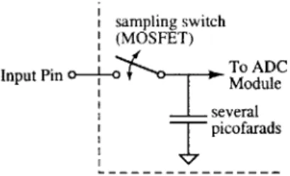
Both ADC converters considered have switched-capacitor analog inputs. A
MOS-FET acts as a sampling switch which connects and disconnects the input to a
sam-pling capacitor with a value between 1 pF and 30 pF. Figure 4-4 illustrates a typical
sampling switch (MOSFET) Input Pin To MoD
several
picofarads
Figure 4-4: Typical switched capacitor input
switched capacitor input. The current spikes caused by the sampling capacitor being connected to the input can not be corrected by an op-amp alone. Glitches caused
by the sampling capacitor in the input voltage will cause erroneous conversions and
corrupt data from the ADC.
The ideal solution is to create a charge reservoir at the input by connecting a large (typically 0.1 pF) capacitor to it, close to the chip. The current required to charge the sampling capacitor will not change the voltage across the larger filter capacitor.
The input to the ADC will remain stable, and an accurate conversion will result. Unfortunately, most op-amps, especially rail-to-rail output op-amps, cannot directly drive large capacitive loads. Voltage gain in the output stage and the negative phase shift caused by the filter capacitor cause the op-amp to oscillate. The solution is the coupling network shown in Figure 4-5. The 100 Q resistor and 330 pF capacitor
100i
From Op-Amps -A bV To ADC 1O
m-330 pF
3.3 ptF
Figure 4-5: ADC input coupling network
attenuate frequencies above 5 MHz, keeping glitches caused by the sampling capacitor from being fed back to the driving op-amps. The 3.3 pF capacitor provides the charge reservoir necessary to stabilize the input voltage to the ADC. The 10 Q series resistor keeps the op-amp from becoming unstable with such a large capacitive load.
4.1.4
Microcontroller
The microcontroller is the heart of the sampling node. It controls the data acquisition process, the serial communications with the host computer, and the local storage of acceleration data. Choosing a microcontroller is difficult as there are many different manufacturers and models, each with different features.
The PIC16F876 was deemed the most appropriate choice for both its price and features. The entire PIC16 model line offers a simple, easy to program 35-instruction instruction set architecture. The PIC16F87X series of microcontrollers are able to write to their own program memory, allowing for the remote update of the firmware. This series also includes a built-in asynchronous serial port module, as well as an I2C
serial interface, discussed in the sections below.
Microchip's microcontrollers are also relatively inexpensive, and are kept in stock at several major component distributors. The 8051 architecture was considered, but
many 8051 clones do not allow for remote program updates, and most come in pack-ages too large for practical use in this application. The author has also worked extensively with similar microcontrollers in the PIC16 product line in the past.
4.1.5
External Data EEPROM
The external data EEPROM is used to store the samples taken during an experiment. Ideally, the interface would be serial, not parallel, as wires and space on the circuit board are scarce resources. An ideal interface choice is the I2C serial bus. I2C is
a two-wire, short-range serial bus standard invented by Philips for communication between integrated circuits. Microchip makes I2C EEPROMs in a variety of sizes. The 24LC515 is a 512 kilobit device that meets the storage requirements detailed in section 3.4. It comes in an 8-pin wide small outline package, which fits easily on the circuit board.
4.1.6
RS-485 Serial Bus Transceiver
The RS-485 transceiver is responsible for converting the 5 V logic levels used by the PIC's on-board serial port to the differential RS-485 signal. It is also responsible for tristating the bus drivers when in receive mode so that another transmitter can use the bus. The normal input impedance of an RS-485 transceiver is 12 kQ, allowing for a maximum of 32 nodes to be connected to the bus. By using a hi-impedance RS-485 driver, that number can be more than doubled. A slew rate-limited device to reduce electromagnetic interference from sharp transitions on the bus is also required. The LTC1487 from Linear Technologies is one of many parts available that fit these requirements, and is readily available from a number of electronics distributors.
4.2
Serial Communication Protocol
The RS-485 serial bus is a shared resource. Only one transceiver can actively drive the bus wires at a time, otherwise data corruption results. A command/response
serial protocol is used to ensure that only one node or the host computer is trying to transmit on the bus at any one time.
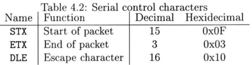
The protocol is packet-based and reserves three special control characters listed in Table 4.2. One is for delimiting the start of packets, one is for delimiting the end of packets, and one is used as an escape character.
Table 4.2: Serial control characters
Name Function Decimal Hexidecimal STX Start of packet 15 OxF ETX End of packet 3 0x03
DLE Escape character 16 OxlO
Figure 4-6 is a diagram of a data packet. The ADDRL, ADDRH, ADDRU, and DATA sections are optional, however the rest of the bytes shown are necessary in a well-formed packet.
The contents of a full packet are illustrated in Figure 4-6, and are discussed in detail below.
Packet
STX STX NADDR CHKSUM ETX
... ...
CMANDI DLEN
Figure 4-6: Packet contents
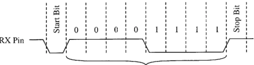
4.2.1 Start of Packet and Baud-Detection
The first two bytes of any packet to be transmitted are two STX characters which mark the start of a packet. Two STX characters are sent in order to allow the baud rate to be auto-detected. When a node receives a byte at the beginning of its receive loop, it counts the number of clock cycles between the first and last rising edges. Using
this count, it can automatically compute the baud rate being used on the serial bus
and configure the baud rate generator module appropriately. Figure 4-7 is a timing diagram detailing this process.
r 0 0 0 0 1 1 1 1
RX Pin
counts cycles between these edges
Figure 4-7: Autobaud timing diagram
After the first STX character, a second is sent to signal the start of a packet.
A one-byte node address is also sent. Each hardware node stores a unique address
in its on-board non-volatile EEPROM storage, which is loaded during the power-on sequence. If a packet's address matches the node's address after the packet is received the node continues to process it. If the address does not match it waits for the next packet. The COMMAND byte identifies a command or action to perform. Available commands are listed in Table 4.3. The DLEN byte is used as a counter for some of the commands, detailed in the section below. DLEN must be non-zero unless a reset command is desired. The ADDRL, ADDRH and ADDRU bytes store addresses for the data transfer commands. A variable length data field comes next. The length is determined by DLEN and the particular COMMAND requested. The CHKSUM byte is the two's complement of the 8-bit sum of all bytes from the address up to the last data byte, inclusive. The ETX byte marks the end of the packet. If the ETX, STX, or DLE bytes appear between the STX or ETX bytes that delineate a packet, they are preceded
by an extra DLE to escape them, to avoid a framing error.
Once a node correctly receives a packet addressed to it, it carries out the requested command and responds with a similar packet to either return the requested data or to indicate the reception of the command packet. After the response packet is sent, the node frees the RS-485 bus and the host computer is free to transmit another packet.
4.3
Node Firmware
The firmware installed on every node is split into two different parts, the bootloader and the user program. Both programs implement the serial communication protocol described in Section 4.2, and a subset of the commands listed in Table 4.3. Hav-ing separate program code spaces allows the samplHav-ing firmware on each node to be updated remotely from the surface.
4.3.1
Bootloader
One reason the PIC16F876 microcontroller was chosen as the development platform is its ability to rewrite its program memory. This allows self-updating code to be written for the device. As discussed in section 3.5, remote updates are a necessity for this system because the nodes will be embedded in potting compound in a pipe section, and will be physically unavailable for manual repair and updates.
A small, well-tested piece of software that runs at startup called the bootloader
is responsible for providing command functionality to allow for remote updates. The bootloader implements the first six commands in Table 4.3, as well as a special reset command, described below. The assembly code for the bootloader can be found in Appendix D.
Command: Reset
The Reset command, implemented in both the user firmware and the bootloader causes the microcontroller to reset itself, and begin execution from the beginning of the bootloader. To select this command, a packet with DLEN set to zero should be sent to the node to be reset. For this reason, any valid packet which is not a reset command should have a DLEN field not equal to zero.
Command: ReadVersion
The ReadVersion command returns two bytes in the data segment of the response packet. This command is implemented in both the bootloader and the user firmware.
If the most significant bit is zero, the device is currently in bootloader mode. If it is
set, the node is in user mode. The remaining fifteen bits make up major and minor version numbers which can be used to keep track of which software revision is running on the node.
Command: WriteProgMem
WriteProgMem is a command used to write to the program memory on the micro-controller to update the user program on the sampling node. It is given DLEN words in little-endian order to write to the program memory address specified in the ADDR bytes of the packet. Little-endian order means placing the least significant byte be-fore the most significant bytes of a multi-byte number. This byte order is used on Intel machines, on which the host computer software was developed. Writes to pro-gram memory must be aligned on 4-word (8-byte) boundaries. This allows newer PIC devices that only support writing the program memory in 4-word blocks to be supported easily in the future.
Command: ReadProgMem
The ReadProgMem command is the companion to the WriteProgMem command. It reads DLEN words from the microcontroller's program storage EEPROM, and returns it in the response packet. This command's intended use is to verify that a user program code update is successful.
Command: WriteEE
This command is used to write DLEN bytes of data from the packet to the data EEPROM on the microcontroller. This is in a separate memory space from the program memory. Writes to the internal EEPROM of the microcontroller can be used to effect a change of address for a node. Care must be taken that the new address does not exist on the serial bus already, otherwise potentially damaging bus collisions could occur. This can also be used to write persistent configuration data to each device, such as calibration data.
Command: ReadEE
This command reads DLEN bytes from the data EEPROM memory on board the microcontroller. This can be used to verify that an address change was successful, or to read other persistent configuration parameters that may be stored in the node's EEPROM.
Command: DoRVReset
This command is implemented in both the bootloader and the user firmware. It causes the node to restart at the user firmware entry point. This is useful for getting address, or other configuration changes, to take effect. A simple response packet is sent to let the host computer know the reset was successful.
When the user code starts, it becomes responsible for handling all serial commu-nication. Commands that are implemented by the bootloader are no longer available, unless a real reset is performed. The most significant bit in the version allows the host computer to query a node to find out what state, bootloader or user, it is in. Thus, an appropriate reset command can be carried out before attempting to use a function unimplemented in the current mode.
4.3.2
User Firmware
The bootloader exists primarily to provide services that allow the host software to update the user firmware and perform other maintenance tasks. The user code is responsible for providing the ability to sample and store data, and to transmit it back to the surface.
As section 4.3.1 mentioned, the user code implements the DoRVReset and Read-Version commands, but none of the read/write commands that modify the microcon-troller's internal memory stores. This is an attempt at program and data memory security, to keep the user program from writing to the program or internal data mem-ory, and corrupting it. The assembly code for the user firmware can be found in Appendix E.
Command: SetSampleCookie
An experiment is defined as the collection of a single data set at a particular sample rate, and the transmission of those data back to the surface. During an experiment, every node on the bus must take a sample at the same time in order for accurate studies of mode shapes to be performed. The sampling clock for the entire bus must be derived from a single node. The node which generates the sampling clock is said to hold the sampling cookie. Section 4.5 covers the sampling process in more detail. The SetSampleCookie command is used to indicate to a node if it does or does not have the sample cookie. If the first byte in the data section of the packet is OxAA, then the node assumes it is to generate the sampling clock. Otherwise, the node expects to be a slave node during sampling, and listens for the sample trigger byte on the serial bus.
Command: Get SampleCookie
This command is used to ensure that only one node holds the sampling cookie before an experiment begins. If more than one node has its cookie bit set at the time of an experiment, bus contention will occur when sampling begins. This can cause asynchronous sampling or missed samples, and can damage the RS-485 drivers on the boards.
Command: Set/GetNumSamples
During an experiment each node maintains a count of how many samples it has taken. Once it reaches the 24-bit number set by SetNumSamples, the node exits sampling mode, and returns to the serial packet receive/response routine. GetNumSamples is used to verify that every node has the correct number of samples set before an experiment begins.
Command: Set/GetSampleRate
The node which holds the sampling cookie generates the sampling clock using the onboard 16-bit TMR1 on the microcontroller. The value used to reset the timer, which determines the sampling period, is set/read by SetSampleRate and GetSampleRate, respectively.
Command: EnterSampleMode
Once an experiment is configured, each node is sent this command. Once a node enters sampling mode, it must complete an experiment. After sending a response packet to the EnterSampleMode command, the node waits to receive five STX bytes in a row. In this way other packet-based transfers can occur on the bus without causing a node to start sampling data (because only 2 STX bytes every appear in a row in any packet transmission). Once every node has received and responded to the the EnterSampleMode command, the host computer sends five STX bytes, and the experiment begins. See section 4.5 for information on sampling process during an experiment.
Command: Start/GetMemoryPage
In order to increase the utilization of the serial bus transactions when uploading exper-iment data to the host computer the data retrieval functions have been pipelined. It takes a significant amount of time to read data from the external EEPROM. Reading
128 bytes with a 384.6 kHz clock takes at least 2.6 ms, time enough to send another 33
bytes on the serial bus. If the page read size is larger, this wasted time grows as well. Consequently, reading a memory page is split into two operations. StartMemoryPage sets the length and address of the block to be read. The node responds immediately with an acknowledge packet, and then reads the requested memory page into internal
memory, while the host computer is triggering page reads on other nodes.
After the node has acquired the page from the external EEPROM, the host com-puter sends a GetMemoryPage request, and the node sends the page back from its
fast internal RAM, increasing the utilization of the serial bus during data upload.
Command: TakeSendSample
This is primarily a debugging command which causes the node to take one sample from both accelerometer channels and send it back to the host computer. Note that the ADCs used will output the result from the last conversion, not the one triggered
by reading a sample from it. To get a current result, two TakeSendSample commands
must be executed in a row. The value returned by the second command issued is the result from the conversion triggered by the first command.
Command: Get/SetOSR
The LTC2440 ADCs used can have their over-sampling ratio programmed via the serial bus. This command allows the host computer to select the particular OSR to be used for the current experiment, or to determine the current OSR being used by
a particular node.
Command: GetEOC
The LTC2440 continuously samples the input over a conversion period. Since the microcontroller reads data from the converter very close to the output rate, it is
possible that a conversion could still be in progress when the microcontroller tries to read a sample. The end of conversion (EOC) output of the ADC is monitored during an experiment. After an experiment is finished, the host computer can use GetEOC to determine if this error occurred. If so, the timer reset value that controls the sampling rate can be modified using the SetSampleRate command to increase the
sampling trigger period.
4.4
Host Computer Software
The host computer software is a program used to communicate with the sampling nodes over the serial bus. It is written in C, and uses the Gimp Tool Kit (GTK)
widget set to provide an easy to use graphical user interface. The software allows the user to update the user firmware on the sampling nodes on the bus. It also allows the user to easily set-up and run experiments, through a simple point-and-click interface. The sample rate and the number of samples is selected. The user clicks 'OK', and the software sets up the serial bus to take data, has the nodes collect the samples, and downloads the data to files in the host computer. It also stores data about each experiment and can export the data as comma separated value or Matlab files for import into popular signal processing programs. A planned enhancement is an integrated experiment browser, that provides an Explorer-like interface to the experiments stored on disk.
4.5
Sampling Process Overview
The first step in initiating an experiment is to set the sampling parameters for all of the nodes. Figure 4-8 shows the window used to set these values. The first option
1:,lPipeHost-exe IW
File _Edit Actions
Nodle Vie-- Experiment SetUp/Run Past Experimens Default Sample Rate (Hz): 220 Hz
Number of Samples 8800
Duration 0:40
Est. Download Time 020
Test Name Experiment 6251 Run Experiment
Figure 4-8: Experiment setup window
is the sampling rate. The LTC2440 ADC is capable of several different oversampling ratios and data output rates. This dialog box allows the user to select the particular OSR/data rate that is best for the particular experiment being run. The user must also select the number of samples to be taken. For data output rates lower than
220 Hz, a software-configurable gain of powers of two could be added, because the LTC2440's resolution exceeds 16 bits for these lower data rates. This is not currently implemented in the prototype node software. The comments in the TakeSample procedure in the user assembly code found in Appendix E describe how this feature may be added to the prototype. The number of samples together with the sample rate determines the length of the experiment. Once these two parameters are set, 'Run Experiment' can be selected.
Figure 4-9 is a flow chart that outlines the sampling process. Before an experi-ment starts, the host computer sets the number of samples on each node and ensures that only one node on the bus has the sampling cookie. By default the node with the lowest address on the bus is given the sampling cookie. The user may select a different node to hold the cookie from the serial bus view screen, shown in Figure 4-10. The timer reset value is computed and set on the node with the cookie. Every node is sent the EnterSampleMode command, and five STX bytes are written to the bus. At this point the sampling process is taken over by the node that holds the sampling cookie.
During the sampling process, the cookie node waits for its timer to overflow, indicating that a sample should be taken. It takes control of the serial bus, and sends a DLE byte. Every node monitors the serial bus for a falling edge caused by the start bit of the DLE. On this falling edge each node takes a sample and stores it into the external data EEPROM. The DLE byte is removed from the serial receive buffer, the number of samples counter is decremented, and every node continues to wait for the next falling edge on the serial bus. When all the samples have been taken, the nodes return to the packet reception routine. As mentioned in section 4.3.2, the first sample taken from the ADCs is old, and should be discarded. Each node throws away the first sample it takes, and does not store it in the data EEPROM.
Using the serial bus as the sampling trigger line offers several advantages. No extra wires besides the power and the two RS-485 lines need to be run in the pipe. Because the RS-485 hardware is designed to accurately carry digital signals long distances, no extra hardware is needed to prevent erroneous samples from being taken. The
User sets
sampling parameters on host computer
I All nodes on bus
'Run Experiment' are updated with
is selected sampling parameters,
one node given the sampling cookie
Five STX bytes written
to bus by host computer, All nodes sent the
beginning the sampling EnterSampleMode command process
Sample cookie node waits for timer to expire, other nodes
wait for DLE byte on bus
Sample cookie node sends a DLE byte to trigger a sample
AE nodes take a sample
First no Store Sample to
Sample? data EEPROM
yes
Last sample no
taken?
yes
Host computer downloadsExeintFisd
data from nodes to disk ExHietFnse
Table 4.3: Serial command definitions Name ReadVersion ReadProgMem WriteProgMem ReadEE WriteEE DoRVReset SetNumSamples GetNumSamples SetSampleRate GetSampleRate SetSampleCookie GetSampleCookie EnterSampleMode StartMemoryPage GetMemoryPage TakeSendSample GetOSR SetOSR GetEOC Value 0 1 2 3 4 5 6 7 8 9 10 11 12 13 14 15 16 17 18 Description
I Bootloader Version IFirmware Version 101 102 0 103 0 104 0 A 1.0 1.0 1.0 1.0 i n 222.173 222.173 222.173 222.173
Figure 4-10: Sample cookie node selection dialog
I I
get firmware version number read a block of program memory write a block of program memory read a block of EEPROM data memory write a block of EEPROM data memory
execute a soft reset to the user code
set the number of samples for an experiment get the number of samples for an experiment set the sample rate for an experiment
get the sample rate for an experiment mark this node as the sample clock
check if this node is set as the sample clock enter the sampling loop
read an external EEPROM block to RAM
send the last page fetched using StartMemoryPage take a single sample and transmit it
get the LTC2440 oversampling ratio set the LTC2440 oversampling ratio see if an End of Conversion error occurred
host computer can also count the DLE bytes that appear on the bus to provide an experiment progress bar for the user.
After all the samples have been collected, the host computer begins issuing Start-MemoryPage and GetStart-MemoryPage requests to nodes on the bus. Data are written in comma separated value (CSV) format to files in the experiment directory, specified in the entry box shown in Figure 4-8. Each node's data are placed in a separate file, named after the node address. The resulting files can be imported into Matlab or Excel for processing later. Data can be written as either raw digital output codes (numbers ranging from -215 to 215 -1), or as float values representing voltages. The
selected output format is chosen in the default configuration dialog, shown in Figure 4-11.
Pip I pions
COM Port: COM2
Default Sample Rate (Hz): 220 Hz
Duration 1:12
Est. Download Time 1:10
Experiment Folder c:\experments Convert Output To Floats
OK
X CancelChapter 5
Results
5.1
Printed Circuit Board
The Eagle automated printed circuit board (PCB) design CAD package was used to design a circuit board that implements the system described in section 4. A complete schematic of the board can be found in Figure B-1. Figure 5-1 is a photograph of a completed prototype. The final circuit board is 0.95" wide and 31" long.
The PCB is composed of four layers. The top and bottom layers are both for routing signals. The two inner layers form power and ground planes which help reduce noise and aid routing signal traces in such a small space. Almost all components used are surface mount technology in order to conserve space. Most of the components were laid out on the top side of the board in order to leave a clear path for the kevlar strength member to run along the bottom.
5.1.1
Layout Considerations
Accelerometer Mount
As the sensitive axes of the accelerometer are in the plane of the chip, it must be mounted in the plane of the cross section of the pipe in order to measure inline and crossflow vibration. Figure 5-2 illustrates how the accelerometer is attached
Main Board, Bottom Side Accelerometer Board
electrii L contac
Assembled Side View
[Ii
solder jointselectrical contacts
Assembled Front View
11r-ri
I : - I
I
Figure 5-2: Accelerometer mounting
to the main circuit board. It is soldered onto it's own PCB which has a tab with solder contacts on one side. This is inserted through a slot on the main board, and the contacts are soldered to each other on the reverse side. Note the accelerometer mounted on the left in Figure 5-1.
Power Planes
The 5 V power plane is split into two separate sections, one for the analog circuitry, and one for the digital components. Each has its own voltage regulator and filter capacitors. This is an attempt to keep the high-frequency digital noise present on the microcontroller's 5 V supply from contaminating the analog supply. The ground plane for both supplies is joined at only one point on the board, to keep large ground
currents on the digital side of the board from affecting the analog ground plane. Figures B-3 and B-4 of the board's copper layers illustrates this separation.
5.2
Software Test
The host computer software was successfully compiled and installed on a Windows 98 computer. Communication tests were successful, and multiple prototype nodes were successfully connected together on the RS-485 bus. An RS-232 to RS-485 converter was used to connect the host computer to the RS-485 bus. The 485SD9TB from B&B Electronics was selected for its low cost and ease of use. Example experiments were run using a Hewlett-Packard signal generator as input. Figure 5-3 shows a few exam-ple waveforms captured with the sampling hardware.
ADC Output(Volts) N 0 0 0.1 0.2 0.3 0.4 4A N I I.O -40 0 0 0.1 0.2 0.3 0.4 4A 0 0.1 0.2 time (seconds) (D N M tO C'j 0.3 0.4 4 2 0 -2 -4 0 4 2 0 -2 -4 0 4 2 0 -2 -4 0
The ability to remotely update
ADC Output(Volts) 0.1 0.2 0.3 0. 0.1 0.2 0.3 0. 0.1 0.2 time (seconds) 0.3 0.4
Figure 5-3: Captured test traces
the user program was also successfully implemented and tested on the prototype.
4 2 0 2 -2 -4 as C,, N 3: LO 2 0 -2 .4 4 U) Csj 2 0 -2 -4
LIXJX\JF\VVTYT\TV\J
Chapter 6
Future Work
Several problems exist in the final design of this prototype. Data transmission, alias-ing and ADC selection, and board size/layout are all issues that should be addressed in future versions of this data acquisition system.
6.1
Data Transmission
The RS-485 serial bus was chosen because it allows for a large number of devices to be connected together on long wire lengths using only two signal wires and a common ground connection. The specification allows for speeds up to 10 Mbps. However, the maximum speed of most RS-232 serial ports on computers today is only 115 kbps or, at most, 230 kbps.
For example, assume that a 60 second long experiment has just been run, sampling at 250Hz. Each node has
samples bits
250 -60 sec -32 = 480000 bits
sec sample
to upload to the host computer. With 50 nodes on a 115 kbps connection, this can take up to four and a half minutes, not including the serial protocol overhead. Waiting five minutes or more for the data from a one minute experiment is unacceptable, especially when experiment time on a boat is being billed.