Publisher’s version / Version de l'éditeur:
The Journal of Physical Chemistry C, 122, 25, pp. 13803-13814, 2018-03-01
READ THESE TERMS AND CONDITIONS CAREFULLY BEFORE USING THIS WEBSITE. https://nrc-publications.canada.ca/eng/copyright
Vous avez des questions? Nous pouvons vous aider. Pour communiquer directement avec un auteur, consultez la
première page de la revue dans laquelle son article a été publié afin de trouver ses coordonnées. Si vous n’arrivez pas à les repérer, communiquez avec nous à PublicationsArchive-ArchivesPublications@nrc-cnrc.gc.ca.
Questions? Contact the NRC Publications Archive team at
PublicationsArchive-ArchivesPublications@nrc-cnrc.gc.ca. If you wish to email the authors directly, please see the first page of the publication for their contact information.
NRC Publications Archive
Archives des publications du CNRC
This publication could be one of several versions: author’s original, accepted manuscript or the publisher’s version. / La version de cette publication peut être l’une des suivantes : la version prépublication de l’auteur, la version acceptée du manuscrit ou la version de l’éditeur.
For the publisher’s version, please access the DOI link below./ Pour consulter la version de l’éditeur, utilisez le lien DOI ci-dessous.
https://doi.org/10.1021/acs.jpcc.8b00910
Access and use of this website and the material on it are subject to the Terms and Conditions set forth at
UV-initiated Si–S, Si–Se, and Si–Te bond formation on Si(111):
coverage, mechanism, and electronics
Hu, Minjia; Hauger, Tate C.; Olsen, Brian C.; Luber, Erik J.; Buriak, Jillian M.
https://publications-cnrc.canada.ca/fra/droits
L’accès à ce site Web et l’utilisation de son contenu sont assujettis aux conditions présentées dans le site
LISEZ CES CONDITIONS ATTENTIVEMENT AVANT D’UTILISER CE SITE WEB.
NRC Publications Record / Notice d'Archives des publications de CNRC:
https://nrc-publications.canada.ca/eng/view/object/?id=84fc28d3-85c7-4577-a379-127710890e98 https://publications-cnrc.canada.ca/fra/voir/objet/?id=84fc28d3-85c7-4577-a379-127710890e98
UV-Initiated Si−S, Si−Se, and Si−Te Bond Formation on Si(111):
Coverage, Mechanism, and Electronics
Minjia Hu,
†,‡Tate C. Hauger,
†,‡Brian C. Olsen,
†,‡Erik J. Luber,
†,‡and Jillian M. Buriak
*
,†,‡†
Department of Chemistry, University of Alberta, 11227 Saskatchewan Drive, Edmonton, AB T6G 2G2, Canada ‡
National Institute for Nanotechnology, National Research Council Canada, 11421 Saskatchewan Drive, Edmonton, AB T6G 2M9, Canada
*
S Supporting InformationABSTRACT: Diaryl and dialkyl chalcogenide molecules serve as convenient precursors to silicon−chalcogenide bonds, Si−E−R groups, on silicon surfaces, where E = S, Se, and Te. The 254 nm light, coupled with gentle heating to melt and liquefy the chalcogenide precursors for 15 min, enables formation of the resulting silicon−chalcogenide bonds. R groups analyzed comprise a long alkyl chain, octadecyl, and a phenyl group. Quantification of substitution levels of the silicon-hydride on the starting Si(111)−H surface by an organochalcogen was determined by XPS, using the
chalcogenide linker atom as the atomic label, where average substitution levels of ∼15% were found for all Si−E−Ph groups. These measured substitution levels were found to agree with 2-dimensional stochastic simulations assuming kinetically irreversible silicon−chalcogen bond formation. Due to the small bond angle about the chalcogen atom, the phenyl rings in the case of Si−E−Ph effectively block otherwise reactive Si−H bonds, leading to the observed lower substitution levels. The linear aliphatic dialkyl disulfide version, Si−S−n-octadecyl, is less limited by steric blocking of surface Si−H groups as is the case with a phenyl group and has a much higher substitution level of ∼29%. The series, Si−S−Ph, Si−Se−Ph, and Si−Te−Ph, was prepared to determine the effect of chalcogenide substitution on the electronics of the silicon, including surface dipoles and work function. The electronics did not change significantly from the starting Si−H surface, which may be due to the low level of substitution that is believed to be caused by steric blocking by the phenyl groups, as well as the relatively similar electronegativities of these elements relative to silicon.
■
INTRODUCTIONControl of the electronic properties of a semiconductor surface is critical for device applications.1−3 Functionalization of a semiconductor surface will affect various fundamental proper-ties of the material, including band bending, an effect that has seen much attention for various semiconductor contacts ranging from metals, solutions, vacuum, and covalently bound molecules.4−7 When a semiconductor device becomes small (on the nanoscale), the surface:bulk ratio increases dramati-cally, and thus surface functionalization can dominate the electronic properties.8−10For a given semiconductor, doping density and type determine the Fermi level relative to valence and conduction bands in the bulk.11,12 In the case of a molecular monolayer covalently bound to a semiconductor surface, a new energy level at the interface is created due to hybridization of the semiconductor and molecule. Band bending and alignment alter both work function and electron affinity of the surface, thus creating surface dipoles that can enhance or attenuate the ability to extract electrons from the surface.13 The complete energy band diagram can be determined using a combination of X-ray photoelectron spectroscopy (XPS) and ultraviolet photoelectron spectroscopy (UPS).4,6,12,14
Among various substrates developed for molecular elec-tronics, silicon is of particular interest not only due to its ubiquity in microelectronics but also due to the feasibility of interfacing organic molecules through direct, covalent bonds on the silicon surface.15 Much attention has been focused on silicon surfaces functionalized with monolayers bound through Si−C bonds,16−18 and experimental results have been complemented by many theoretical studies.6,19,20 Systematic preparation and evaluation of other covalent bonds on silicon are, however, much more limited, but equally intriguing. Computational DFT work has suggested that the nature of the atom through which an organic monolayer is bonded to a silicon surface, the headgroup, can have profound effects on underlying electronics of the silicon.21−23These predictions for chalcogenides have not yet been tested experimentally.
The chemistry of organic molecules bound to silicon surfaces through silicon−chalcogen bonds on surfaces is relatively new Special Issue: Prashant V. Kamat Festschrift
Received: January 26, 2018
Revised: February 28, 2018
Published: March 1, 2018
pubs.acs.org/JPCC
Cite This:J. Phys. Chem. C 2018, 122, 13803−13814
and has been focused for the most part on sulfur-containing molecules. Functionalization of silicon with organosulfur compounds, resulting in surface-bound silicon−sulfur bonds, was first initiated under ultrahigh vacuum conditions.24 More recently, solution-phase approaches toward silicon−sulfur bound alkyl monolayers were shown to be accessible through reactions of alkanethiols, driven by UV,25,26 white light,27 or heat.14,28 Using heat and supercritical carbon dioxide as an alkanethiol carrier fluid, monolayers on silicon surfaces bound through Si−SR bonds were shown to be stable to prolonged exposure to ambient atmosphere.29To access silicon−selenium bonds, Bocian and co-workers used a very short (2 min), high-temperature (400 °C) baking procedure to covalently attach acetylchalcogenidoarene-derivatized (Ar-EAc, E = S, Se) porphyrins on Si(111) surfaces through Si−O, Si−S, and Si− Se linkages.30,31However, until recently the complete series of S, Se, and Te linkers remained elusive due to the difficulty of making Si−TeR bonds.
In order to secure the Si−Te bond and complete the series of chalcogenides, we turned to diorganodichalcogenides (REER, where E = S, Se, Te) as synthetically useful molecular precursors.32,33 These molecules are readily available both commercially and synthetically and have a weak dichalcogenide bond that can be easily cleaved to enable silicon surface functionalization through radical-based mechanisms. Diorgano-disulfides and diselenides react with porous silicon at room temperature with a diazonium radical initiator, but these conditions are incompatible with diphenyl ditelluride due to its lower solubility.33Diorganodichalcogenide molecules, however, very efficiently and cleanly form Si−ER bonds (E = S, Se, and Te) on high surface area hydride-terminated porous silicon through microwave heating (10−15 s) or direct thermal heating (230 °C, 2 min), temperatures at which silicon radicals are generated directly through homolytic Si−H bond cleavage.32 Extension of this chemistry from porous silicon to flat Si(111)− H surfaces with these heat-driven approaches failed due to severe contamination with other decomposition products of the diorganodichalcogenide molecules (vide infra). In this work, we describe chemistry to functionalize Si(111)−H surfaces with Si−ER bonds (E = S, Se, Te), in a manner that is fast and free from both oxidation and contamination from decom-position products of the starting diorganodichalcogenide molecules (Scheme 1). A combination of mild heating and UV irradiation resulted in a “sweet spot” of desired reactivity to enable clean functionalization of silicon with a series of Si− S−Ph, Si−Se−Ph, and Si−Te−Ph groups. Both the substitution levels and electronic properties of these surfaces were analyzed via XPS. This method was also used with a saturated aliphatic variant, Si−S−n-octadecyl.
■
MATERIALS AND METHODSGeneral.Si(111) wafers (n-type, phosphorus doped, 1−10 Ω·cm, 525 ± 25 μm) were obtained from Virginia Semi-conductor, Inc. Diphenyl disulfide (99%), diphenyl diselenide (98%), and diphenyl ditelluride (98%) were purchased from Sigma-Aldrich. Di-n-octadecyl disulfide (98%) was purchased from Alfa Aesar. All reagents were stored in a −20 °C freezer inside an argon-filled glovebox. Dichloromethane was purified by a solvent purification system (Innovative Technology, Inc.) and dried over molecular sieves for 24 h in glovebox prior to use. Molecular sieves (type 4A, 1/16 in. pellets, for selective adsorption), NH4OH (aqueous, 30%), and HCl (aqueous,
37%) were purchased from Caledon Laboratories, Ltd. NH4F
(aqueous, 40%, semiconductor grade) was purchased from Transene Company, Inc. H2O2(aqueous, 30%) and 2-propanol
(≥99.5%) were obtained from Sigma-Aldrich. KAuCl4·xH2O
was purchased from Strem Chemicals. HF (49% aqueous, semiconductor grade) was purchased from J. T. Baker.
Flat Si(111)−H Preparation. Silicon wafers were cut into 1 cm × 1 cm squares using a dicing saw (Disco DAD 321) and then sonicated in 2-propanol for 10 min. Each chip was cleaned by a standard RCA procedure: the chips were first immersed in a fresh solution of H2O/30% NH4OH (aq)/30% H2O2 (aq)
(6:1:1) at 80 °C for 10 min, rinsed with water, and then immersed in a fresh solution of H2O/37% HCl (aq)/30% H2O2
(aq) (5:1:1) at 80 °C for another 10 min. The chips were rinsed with water and dried with a stream of argon gas. The cleaned silicon chips were immersed in argon-saturated 40% NH4F for 5 min and then dipped into deionized water for 10 s.
After being dried with an argon stream, each chip was immediately transferred into a glovebox via a sealed argon-filled vial.
Reactions with Dichalcogenides.All reactions except for the etching of silicon surfaces were performed in the argon-filled glovebox. Each of the dichalcogenides, including diphenyl disulfide (PhSSPh), diphenyl diselenide (PhSeSePh), diphenyl ditelluride (PhTeTePh), and di-n-octadecyl disulfide (C18SSC18), was dissolved in dichloromethane to form a
solution with a concentration of 20 mg/mL. The 1 cm × 1 cm silicon chip was placed on a hot plate heated to 80 °C, in the glovebox. 40 μL of a specific dichalcogenide solution was dropped onto the silicon and then covered with a UV grade quartz disc (from University Wafer), forming a sandwich of quartz coverslip−chalcogenide reagent−silicon wafer (assembly process is shown in Figure S1). The dichloromethane evaporated immediately upon contact with the silicon because of its low boiling point, and the small volume of the solution spread over a large area, leaving a solid film between the quartz and silicon. The melting points of PhSSPh, PhSeSePh, PhTeTePh, and di-n-octadecyl disulfide are 61 °C, 61 °C, 66 °C, and 62 °C, respectively, and thus the chalcogenide compounds melted to form a film. The samples were then irradiated with the light from a UVP Pen-Ray lamp (254 nm, model 11SC-1) held 1 cm above the samples for 15 min. The intensity of 254 nm light reaching the quartz surface was Scheme 1. Overall Reaction Scheme Summarizing the Formation of Si−S, Si−Se, and Si−Te Bonds on Si(111)−H Surfaces
measured to be ∼2 mW cm−2. After reactions, the quartz coverslip was removed, and the silicon chips were soaked in dry dichloromethane for 3 min, followed by three rinses with a stream of dichloromethane from a pipet, to remove the unreacted reagents. The samples were removed from the glovebox in sealed vials, dried further under an argon gas stream, and analyzed immediately.
Analytical Techniques.X-ray photoelectron spectroscopy (XPS) spectra were taken on a Kratos Axis Ultra X-ray photoelectron spectroscopy system with a power of 14 kV, 12 mA, and 168 W using an Al source with an energy of 1487 eV, in the University of Alberta NanoFAB, with binding energies calibrated to Au 4f7/2= 84.0 eV. Photoelectrons were collected
using a takeoff angle of 90° relative to the sample surface. Although samples were not rotated during XPS measurements (to eliminate photodiffraction effects), multiple measurements of identically prepared samples in separate XPS runs were used for all quantitative XPS calculations. From these results, it was found that there was generally less than a 10% difference in calculated substitution levels. Ultraviolet photoelectron spec-troscopy (UPS) spectra were taken on a Kratos Axis Ultra XPS system with a power of 3 kV, 20 mA, and 60 W. Advancing and receding contact angle measurements were taken on an FTA200 video system. Sessile drop contact angles for the stability monitoring of the functionalized silicon surfaces were measured using 3 μL of water on a Ramé-Hart Mode 100−00 contact-angle goniometer. Film thicknesses were determined by contact mode atomic force microscopy (AFM) scribing. AFM scribing and images were captured using a Veeco/Digital Instruments Multi-Mode NanoScope IV. The intensity of the 254 nm UV light was measured by a Solo 2 energy and power meter with a XLPF12-3S-H2-D0 head (Gentec Electro-Optics Inc.). The resistivity of silicon wafers (oxide layer was removed by HF) was measured using a Keithley 2400 Source Meter in conjunction with a Jandel four-point probe (serial number LB25907) with 0.5 mm probe spacing.
Simulation.Stochastic packing of phenylchalcogenides on the Si(111) surface was simulated by assuming the steric interactions to be 2-dimensional, where the Si−E−Ph groups were represented by the union of two hard disks. The respective radii of these disks were set by using the van der Waals radii of the chalcogen and the phenyl ring. Briefly, the packing algorithm works according to the following procedure. First, a sufficiently large Si(111) surface is generated (results were found to be effectively invariant for more than 14 000 Si atoms), and a random Si site is chosen. Then a Si−E−Ph group is placed at this random Si site, at multiple random orientations with uniform spacing (results were found to be invariant for more than 7 different orientations), and checked to see if it overlaps with any of the other Si−E−Ph groups on the surface. If an orientation with no overlaps is found, it is permanently left in that position and orientation. This process is then repeated at different randomly chosen Si surface sites until all silicon surface sites have been checked. The final substitution level is simply the number of Si−E−Ph groups divided by the number of silicon sites. The substitution levels determined from simulation are the average of 150 independent simulation runs, each having a simulation size of 14 000 silicon sites and checking 13 different orientations for the Si−E−Ph group at each silicon site. It is also noted that the sites at the edge of the simulation volume were not used to calculate the substitution level, as the amount of steric interactions will be lower in these regions. Specifically, sites within three silicon
lattice parameters of the simulation boundaries were not used. Nonetheless, given the large simulation volume, the edge effects were very small, leading to a less than ∼3% difference after edge correction.
■
RESULTS AND DISCUSSIONSilicon−Chalcogen Bond Formation via UV Irradiation and Gentle Heating. To drive selective chemistry on Si(111)−H with dialkyl or diaryl dichalcogenides, low intensity 254 nm UV irradiation was coupled with gentle heating to enable the use of neat molecular reagents, with no additional solvent or other additives. A small volume (40 μL) of dichloromethane solution was placed on a 1 cm2 chip of
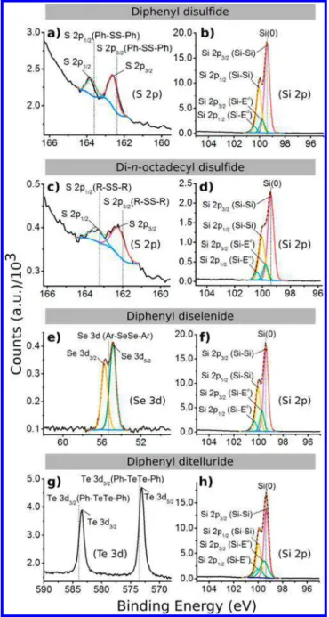
freshly etched Si(111)−H and then heated to 80 °C to evaporate the solvent and melt the film (all four molecules have melting points below this temperature). A quartz window was pressed on top of the melted reagent to spread it evenly over the face of the silicon wafer, as shown inFigures S1 and S2. The sample was then irradiated by a Hg pen-lamp with a wavelength of 254 nm (intensity 2 mW cm−2). X-ray photoelectron spectroscopy (XPS) was carried out on the silicon samples reacted with the PhSSPh, PhSeSePh, PhTeTePh, and di-n-octadecyl disulfide precursors to deter-mine the nature of the bonding atom to the silicon (S, Se, or Te) and the level of oxidation. As shown in Figure 1, the narrow Si 2p feature of all four silicon samples reveals little oxidation, which would appear at a higher binding energy above 102 eV.3,34Figure 1a,c shows the S 2p spectra, revealing the characteristic S 2p3/2and S 2p1/2peaks at 162.6 and 163.8 eV,
for the PhSSPh-functionalized silicon surface, respectively, and 162.5 and 163.7 eV, for the di-n-octadecyl disulfide-function-alized silicon surface, respectively. The Se 3d spectrum (Figure 1e) also reveals a doublet of the Se 3d peak that has been fit to Se 3d5/2 and Se 3d3/2 peaks located at 54.9 and 55.7 eV,
respectively. Two separate Te 3d peaks (Figure 1g) with binding energies of 573.1 and 583.5 eV correspond to Te 3d5/2
and Te 3d3/2, respectively. The binding energies for these
chalcogens agree with the previous results for surfaces functionalized with Si−S, Si−Se, and Si−Te bonds on porous silicon surfaces.30,32 The features of the starting reagents, PhEEPh (E = S, Se, Te) and di-n-octadecyl disulfide, are shown inFigure 1and are summarized inTables S1 and S2.
Prior work in our group showed that dialkyl and diaryl dichalcogenides react very rapidly (seconds to minutes) and cleanly with hydride-terminated porous silicon at high temper-atures in the range of 200−230 °C under inert atmosphere to form Si−E−R (E = S, Se, Te) groups with no apparent oxidation.32 On flat Si(111)−H, however, contamination was determined by XPS to be a serious issue in the case of the tellurium derivative. Thermally driven reactions with diphenyl dichalcogenides on Si(111)−H were first carried out at 200 °C for 90−120 s. The XPS spectra, shown inFigures S3a, b, c, and d, for the reactions with diphenyl disulfide and diphenyl diselenide on silicon surfaces proceed with little contamination or oxidation. For diphenyl ditelluride, however, the Te 3d XPS spectrum is complicated by two sets of Te 3d doublets, as seen inFigure S3e, as well as oxidation of the silicon surface (feature at 103 eV inFigure S3f). Lowering the temperature to 150 °C also resulted in oxidation of the silicon surface (Figures S3g and h). The set of doublets with a higher binding energy is consistent with the formation of Te−O bonds.35Previous work has shown that phenylchalcogenides decompose upon heating to yield chalcogenide metal due to cleavage of the
chalcogenide−phenyl bond.36While the reactions were carried out in an inert atmosphere glovebox (O2< 1 ppm), if Te(0)
was indeed formed under these conditions, brief exposure of the surfaces to air upon loading them into the XPS could result in oxidation of the tellurium metal. In order to keep the chemistry consistent across the sulfur, selenium, and tellurium derivatives, mild UV irradiation combined with gentle heating to 80 °C was used throughout this work.
Contact angle measurements of functionalized surfaces are typically used to obtain information regarding surface energy,37 monolayer order,38and kinetics.39Static and dynamic (θa/θr)
water contact angles of all the freshly prepared diphenyl dichalcogenide-functionalized samples fall between 80° and 83° (Table S3 and Figure S4), which are very close to that of the starting hydride-terminated silicon surface (∼83°) and hence
not an informative metric to quantify surface functionalization. As such, the aliphatic disulfide, di-n-octadecyl disulfide, was used to provide insights into the rate of the reaction.39−41As shown inFigure 2, the Si(111)−H surface reacted with
di-n-octadecyl disulfide at 80 °C with UV irradiation appears to follow classic Langmuir kinetics,42 and a maximum contact angle of ∼105° is reached after 10 min, a value similar to that of other silicon surfaces functionalized with long alkyl chains (contact angles range from ∼105° to 110°).43−45 Representa-tive contact angles of phenyl- and long alkyl chain-terminated silicon and gold surfaces from the literature are shown inTable S4. Control experiments, summarized inTable S5, showed that both heat and UV irradiation are necessary to reach this high contact angle with di-n-octadecyl disulfide. With only heat (80 °C) or UV irradiation, the contact angles fell within the range of 83−88°, indicating that both are required to enable the reaction to proceed to high coverage within 15 min. With hexadecane as the probe liquid for contact angle measurements, the contact angles of all Si−E−Ph surfaces were low (θ < 10°), while for the Si−S−n-octadecyl surface, the average contact angle was 43.4° (Table S3), a value that is consistent with previous work investigating monolayers on silicon,46 gold,47or hydroxylated silicon surfaces.48
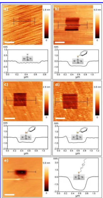
Determination of Layer Thickness. Thicknesses of the resulting films were measured by scribing with an AFM tip, a commonly used technique that can be used to remove soft organic monolayers from the hard inorganic surface by scratching the surface with a (hard) silicon AFM tip.49−52 The scratched hydride-terminated silicon surface inFigure 3a reveals a small height difference of ∼0.2 nm, most likely due to physisorbed hydrocarbon contaminants upon exposure to laboratory ambient. As shown in Figure 3b−d, the scribed areas of the diphenyl dichalcogenide-treated surfaces, capped with Si−E−Ph groups, are ∼0.8 nm deep, as determined from both line profiles and histogram analysis. For the Si− S−n-octadecyl-terminated surface, the measured depth is ∼2.5 nm; a smaller area could only be scribed due to buildup of residue on the AFM tip.
In order to calculate the predicted thickness of the molecular layer on the Si(111) surface, the Si−E bond length, the size of the phenyl ring, and the Si−E−C bond angle need to be known or assumed. The value with the greatest uncertainty is the bond angle about the chalcogen, the Si−E−C bond angle; a table of comparable molecules is provided inTable S6.
Figure 1.XPS spectra of Si(111) surfaces after the UV-mild thermal (80 °C) treatment with indicated diphenyl dichalcogenides and di-n-octadecyl disulfide reagents for 15 min. Orange dashed curves are the envelope fittings. The data from this figure and supporting literature are tabulated inTables S1 and S2. Ea= S, Se, Te, as well as H.
Figure 2. Water contact angles of di-n-octadecyl disulfide-function-alized silicon surfaces with different reaction times (black dots) and the fitting curve according to the contact angle data (red curve). Each black dot represents a unique sample that had been reacted for the indicated reaction time. The error bars represent the standard deviation of five measurements on the same sample.
Only a small number of molecules with silicon−chalcogenide bonds has been sufficiently characterized to evaluate bond angles (by single-crystal X-ray diffraction, for instance). For instance, the Si−S−H bond angle in tri(mesityloxy)silanethiol has been reported to be 95.4°,53and that of Si−S−CH3in the
S-methyl ether of tritbutoxysilanethiol is 106°,54both of which were determined from crystal structures. For thioethers, the C− S−C bond angles for both Ph−S−CH3 and Ar−S−Ar
molecules are around 100°∼104°.55−59Selenoethers, Ar−Se− Ar and C(sp3)−Se−C(sp2), have a C−Se−C bond angle of
∼101°.60,61 The C−Te−C bond angle for the telluroethers, Ph−Te−CH3 and Ph−Te−Ph, is ∼96°.62 When Si−E−C
bond angles of 103°, 101°, and 96° were imposed upon Si−
S−Ph, Si−Se−Ph, and Si−Te−Ph groups on the Si(111)−H surface, severe steric interference between under-lying Si−H groups and the overunder-lying phenyl rings resulted. As shown in the space-filling representations inFigure 4, only
when the bond angle about the chalcogenide of the Si−E− Ph was increased to 125° (Si−S−Ph), 124° (Si−Se−Ph), and 117° (Si−Te−Ph) was there no overlap of the van der Waals radii of the phenyl rings and the underlying Si−H groups. The higher angle of the Si−S−Ph group results from having the shortest Si−E bond of the trio, as it needs to have a higher tilt to avoid overlap with the underlying silicon hydrides. These calculations are summarized inScheme 2and are shown with the smallest possible angle about the chalcogen atom. The calculated thicknesses for the Si−E−Ph surfaces therefore represent the thinnest possible monolayerwith a higher angle about the chalcogenide linker atom, the monolayer could be thicker. For the aliphatic variant, the Si−S−n-octadecyl-terminated surface, a tilt angle of the n-octadecyl group of 33° from the surface normal was used, based upon prior experimental results by Lou and co-workers for a similar surface formed via the reaction of 1-dodecanethiol on Si(111)− H.26
The calculations inScheme 2differ to a small degree from the results observed by AFM scribing. To repeat, it must be stated that we cannot determine the exact bond angle about the chalcogenide for these Si−E−R-functionalized surfaces, and thus the observed difference of ∼0.2 nm between the calculated thicknesses and the measurements from AFM scribing could be due to physisorbed contamination but could also result from a higher Si−E−C bond angle about the chalcogen. Indeed, it has been claimed that Si−O−Ph-terminated surfaces have a Si−O−C bond angle close to 180° at high substitution levels,63 but for the sulfur, selenium, and tellurium versions, the bond angle for RER molecules decreases going down the chalcogen group, so a bond angle closer to 180° about the chalcogen seems unlikely. Detailed quantification of substitution level by
Figure 3.AFM scribing of Si(111) surfaces. All scale bars are 400 nm. (a) Scribing on a hydride-terminated Si(111) surface. (b−d) Functionalized Si(111) surfaces reacted with PhSSPh, PhSeSePh, and PhTeTePh, respectively. (e) Functionalized Si(111) surfaces reacted with di-n-octadecyl disulfide. A smaller area was etched for the di-n-octadecyl disulfide molecule due to the rapid buildup of residue on the tip.
Figure 4.Side-view space-filling model of the Si−E−Ph (E = S, Se, Te) interfaces on a flat hydride-terminated Si(111) surface. The chalcogenide-based functionalities were placed randomly on the surface, as would be the case for kinetically trapped, irreversible Si− E bond formation.
XPS, complemented by simulations that assume spatially stochastic covalent bonding (kinetic trapping), is described
vide inf ra.
Quantification of Substitution Level of Si−H with Si−ER Groups. While the AFM scribing for all four Si−
E−R surfaces suggests uniform films, quantitative determi-nation of the level of substitution of Si−H groups with chalcogenides was desired. XPS has been previously employed to estimate the substitution level of alkyl groups on silicon, bound through silicon−carbon bonds.64−66 In order to determine the substitution level, Θ, analytical expressions for the relative peak intensities (areas) of the silicon, carbon, and chalcogen signals were first derived. As is conventionally done, the silicon substrate and corresponding alkyl/phenyl molecular overlayers can be approximated by continuum layers that have a uniform atomic density, ρi, electron attenuation coefficient, λi, and thickness di. By making this continuum approximation, the
measured intensity of photoelectrons can be calculated by simple application of the Beer−Lambert law. In the case of a silicon substrate (atomic density, ρSi, electron attenuation
length, λSiSi) with a chalcogen overlayer (atomic density, ρE,
electron attenuation length, λEE) capped by a phenyl/alkyl
overlayer (atomic density, ρC, electron attenuation length, λCC),
the total XPS intensity of the silicon peak is given by
∫
σ ρ λ λ λ σ ρ λ λ λ = − − − = − − ∞ I A x x d d I A d d( exp( / )d )exp( / )exp( / )
exp( / )exp( / )
Si Si Si 0 SiSi E SiE C SiC
Si Si Si SiSi E SiE C SiC
(1)
where A is the areal footprint of the X-ray beam and σSiis the
relative sensitivity factor for silicon. Likewise, the signal from the chalcogen layer is given by
∫
σ ρ λ λ σ ρ λ λ λ = − − = − − − I A x x d I A d d ( exp( / )d )exp( / ) (1 exp( / ))exp( / ) d E E E 0 EE C EC E E E EE E EE C EC E (2)Lastly, the signal from the carbon layer is given by
∫
σ ρ λ σ ρ λ λ = − = − − I A x x I A d ( exp( / )d ) (1 exp( / )) d C C C 0 CC C C C CC C CC C (3)Taking the ratio of the silicon and carbon intensities (eqs 1and 3) gives σ ρ λ λ σ ρ λ λ λ λ = − − − I I d d d exp( / ) (exp( / ) exp( (1/ 1/ )) Si C Si Si SiSi E SiE C C CC C SiC C SiC CC (4)
This expression can be simplified in two ways. First, we can assume that exp(dC(1/λSiC− 1/λCC)) ≈ 1 since the attenuation
length of photoemitted electrons from the silicon layer passing through the carbon layer, λSiC, will be very close to that for
photoemitted electrons from the carbon layer passing through the carbon layer, λCC. Second, we also assume that dE/λSiE≪ 1
since the thickness of the chalcogen layer will be less than twice the van der Waals radius (∼0.4 nm), while the attenuation length of the chalcogen will be on the order of 3−4 nm. From these simplifying assumptions,eq 4becomes
σ ρ λ σ ρ λ λ = − I I (exp( /d ) 1) Si C Si Si SiSi C C CC C SiC (5)
Finally, this expression can be used to calculate the substitution level by determining an effective thickness dCeffof a carbon layer
with attenuation length, λSiCSi , and atomic density, ρCSi, equal to
that of a monolayer with 100% coverage of the silicon (111) Scheme 2. Theoretical Monolayer Thicknesses of Si−S−
Ph−, Si−Se−Ph−, Si−Te−Ph−, and Si−S−n-Octadecyl-Modified Silicon Surfaces Calculated Based upon the Indicated Bond Lengths and Anglesa
aH
vdw is the van der Waals radius of the hydrogen para to the
chalcogenide. Red lines indicate steric hindrance between the phenyl ring and underlying hydrogen atoms on the silicon surface.
surface. The values of λSiCSi and ρCSican be estimated by scaling
the values for gold surfaces with 100% coverage
ρ = n ρ n C Si Si Au C Au (6) λ = n λ n SiCSi Au Si SiC Au (7) λ = n λ n CCSi Au Si CC Au (8)
where nSi and nAu are the atomic surface densities of (111)
silicon (7.8 × 10¹⁴atoms/cm2) and the (√3 × √3)R30 surface
of (111) gold (4.6 × 10¹⁴atoms/cm2). Combiningeqs 5,6,7
and8gives λ σ ρ λ σ ρ λ = ⎛ + ⎝ ⎜⎜ ⎞ ⎠ ⎟⎟ d n n I I ln 1 Ceff Au Si SiC Au C Si Si SiSi Si C CAu CCAu (9)
From eq 9, we can divide the effective thickness by the theoretical monolayer thickness (2.01 nm for Si−S−n-octadecyl at a tilt angle of 33°) to obtain the substitution level. The average substitution level determined using eq 9is 50 ± 2%, which agrees well with previously reported values for hydrosilylation of alkyl chains on the (111) silicon.64,67−70
When using XPS data to determine the substitution level of alkyl chains on a silicon surface, analysis is typically limited to the silicon and carbon photoelectron signals. However, in the case of Si−S−n-octadecyl, we can also utilize the silicon and sulfur peak intensities to derive a second expression for the substitution level. If we divide eqs 1 and 2 we arrive at the following expression σ ρ λ λ λ σ ρ λ λ λ = − − − − − I I d d d d exp( / )exp( / ) (1 exp( / ))exp( / ) Si E
Si Si SiSi E SiE C SiC
E E EE E EE C EC (10)
If we again assume that p(dE(1/λSiE− 1/λEE)) ≈ 1, exp(dC(1/
λSiC− 1/λEC)) ≈ 1, and dE/λSiE≪ 1, we arrive at the simplified
expression of σ ρ λ σ ρ = I I d Si E Si Si SiSi E E E (11)
Given that ρEdE= nE, where nEis the atomic surface density of
chalcogen atoms, and the substitution level is defined as Θ =
nE/nSi, we can solve for the substitution level
ρ λ σ σ Θ = I n I Si SiSi Si E Si E Si (12)
The Si-S-n-octadecyl substitution level determined usingeq 12are found to be 27 ± 6% (seeTable 1), which appears to be significantly different from those determined using eq 9. However, this discrepancy can be resolved by adjusting for the
fact that unavoidable amounts of adventitious carbon will contribute to the integrated peak intensity of the C 1s signal. This can be done by first subtracting the effective thickness of the adventitious carbon layer from eq 9, then calculating the substitution level. Usingeq 9the thickness of the adventitious carbon layer is estimated by utilizing the silicon and carbon XPS spectra for hydride-terminated silicon, Si(111)−H, which is found to be 0.42 ± 0.06 nm (Table S7). After correcting for the additional signal from the adventitious carbon, the substitution level determined using the silicon and carbon signals (eq 9) is found to be 30 ± 4% (Tables 1 and S8), which agrees very well with the values of 27 ± 6% determined using the silicon and sulfur signals [eq 12]. In the case of Si−E−Ph-modified silicon surfaces, the substitution level can be determined using the silicon and chalcogen signals via application ofeq 12. The average substitution levels are all found to be ∼15% (Table 1). For more detailed information on these calculations, all of the utilized constants (Table S10) and intensity ratios measured from XPS can be found in the Supporting Information.
From these data it is found that the substitution level of the Si-E-Ph-modified silicon surfaces (∼15%) is low compared to the aliphatic variant, Si−S-n-octadecyl (∼30%). These lower substitution levels can be better understood by inspection of Figure 4, where the bulky phenyl rings are shown to be nearly parallel to the silicon surface. Such a molecular surface configuration would shield a significant number of Si−H bonds from further reactivity, thereby reducing the maximum possible Si−E−Ph groups that can bind to the silicon surface. In order to better understand/validate the substitution levels measured by XPS,Figure 5a shows an idealized close-packed representation of Si−S−Ph groups on a Si(111) surface. It can be seen from this tiling that the substitution level is 25%, which gives a useful reference for the upper theoretical limit of the substitution level. In reality, this close-packed configuration of Si−E−Ph groups cannot be achieved due to the covalent nature of the silicon−chalcogen bond and the spatially stochastic nature of silicon−chalcogen bonding events. Once Si−E−Ph groups are bonded to the silicon surface they are kinetically trapped and cannot diffuse to other sites in order to achieve a lower energy/more densely packed configuration. As such, there will be a significant fraction of silicon surface atoms that are not bonded to a chalcogen or directly underneath a phenyl ring and are unavailable to form silicon−chalcogen bonds.
This proposed mechanism of spatially stochastic covalent bonding of Si−E−Ph groups on the silicon (111) surface was simulated, where a representative configuration is shown in Figure 5b. In these simulations, the surface packing is assumed to be a 2-dimensional problem, where the Si−E−Ph groups are represented by the union of two hard disks with respective radii corresponding to the bond lengths shown in Scheme 2. Table 1. Substitution Level Measured from XPS Data and Simulation
functional group Si−S−Ph Si−Se−Ph Si−Te−Ph Si−S−n-octadecyl Si−S−n-octadecyl
substitution level (%) (XPS data) 15 ± 1a 13.9 ± 0.6a 16 ± 2a 27 ± 6a 30 ± 4b
substitution level (%) (simulation) 14.9 ± 0.1 14.7 ± 0.1 13.2 ± 0.1 N/A N/A
a,bCalculated using eqs 12 and9, respectively. Substitution levels are displayed as average ± standard deviation. Four identical samples were
prepared for each type of silicon surface. For each sample, two spots were measured by XPS, leading to each functionalization of silicon surfaces containing eight measurements.Table S9includes the substitution level for each measurement. Substitution levels measured from simulation are the mean of 150 independent simulation runs (14 000 Si atoms and 13 different possible orientations for each Si−E−Ph group). Substitution levels marked.
Briefly, the stochastic bonding of Si−E−Ph groups is simulated using the following method. First, a sufficiently large silicon (111) surface is generated (results were found to be effectively invariant for more than 14 000 Si atoms), and a random Si site is chosen. Then a Si−E−Ph group is placed at this random Si site, at multiple random orientations with uniform spacing (results were found to be invariant for more than 7 different orientations), and checked to see if it overlaps with any of the other Si−E−Ph groups on the surface. If an orientation with no overlaps is found, it is permanently left in that position and orientation. This process is then repeated at different randomly chosen Si surface sites until all silicon surface sites have been checked. A time series visualization of a stochastic simulation of Si−E−Ph groups packing the Si(111) surface is shown in Movie S1 in the Supporting Information. The substitution levels measured from these simulations are shown inTable 1and found be ∼15%, which is in excellent agreement with the experimentally measured values
derived from XPS data. These results support the claim of near-parallel configurations of the phenyl rings, as well as the stochastic nature of Si−E−Ph groups bonding to the silicon surface.
Proposed Mechanism.As mentioned earlier, the reaction of a Si(111)−H surface with di-n-octadecyl disulfide with only UV irradiation, or only 80 °C heating, resulted in a small increase of contact angle versus the unfunctionalized hydride-terminated silicon surface (Table S5), indicating that successful functionalization requires that the UV illumination be coupled with gentle heating. The key intermediate in silicon−chalcogen bond formation is most likely a silicon radical formed via homolytic cleavage, as shown in Figure 6, as has been postulated earlier on both surfaces and in silane mole-cules.27,32,33,44,71,72 This silicon radical can then add to the dichalcogenide through an SH2 reaction, followed by collapse of
the trivalent intermediate to product and an organochalcogen radical.32,33,71,72 The silicon radical could also react directly with an organochalcogen radical to form a silicon−chalcogen bond, although this pathway is expected to be less likely due to the improbability of having both species, present in low concentrations, in close proximity.
The central question is the driving force for homolytic cleavage of the surface silicon−hydride bond. The temperature required to initiate productive homolytic cleavage of the Si−H bond is typically in the range of 150−200 °C, as shown through numerous studies on hydrosilylation of alkenes and alkynes on silicon surfaces.45,73,74 Similarly, heating to 80 °C does not induce Si−EC bond formation, as shown by the control experiment with only heat (vide supra); heating to 80 °C appears to only serve to liquefy the chalcogenide molecules to form an even layer on the silicon surface. The 254 nm UV light, however, is of sufficient energy (112.6 kcal/mol) to induce cleavage of both the diaryl/dialkyl dichalcogenide E−E bond75−77 and the Si−H bond.78−82 Because of the high absorption coefficients at 254 nm for the three diphenyl dichalcogenides as well as the di-n-octadecyl disulfide (Figure S5, and corresponding calculations inSupporting Information), essentially all of the incident UV light would be absorbed by this molecular layer, and no UV light would directly impinge upon the silicon surface. The role of the 254 nm UV light, then, must be to cleave S−S, Se−Se, or Te−Te bonds (bond energies of 53−57, 40, and 30−35 kcal/mol, respectively)33,76,77at the surface of the melted REER layer, in close proximity to the quartz coverslip, to yield thiyl, selenyl, or telluryl radicals, RE• (E = S, Se, and Te), respectively, as outlined in Figure 6. Diffusion of these radicals throughout the layer could then lead to formation of silyl radicals, Si•, at the surface, through removal of H• from surface-bound Si−H groups (Figure 6a).
Upon formation of Si• species, two possible pathways would realize the formation of Si−ER bonds, as has been previously described.32 The first route involves stepwise SH2
addition of REER to a silyl radical, producing trivalent sulfuranyl, seleranyl, or telluranyl radical intermediates, followed by collapse of the intermediate to form the final Si−ER product and an RE• radical (Figure 6b). This reaction pathway would most likely be favored due to the high abundance of REER molecules near the surface. The second pathway involves the direct combination of a surface silyl radical Si• and free chalcogenide radical RE• to produce Si−ER (Figure 6c).32Both may be in operation and would be difficult to distinguish.
Figure 5. (a) Idealized close-packed configuration of Si−S−Ph groups on a Si(111) surface. (b) Configuration resulting from a simulation of stochastically packed Si−S−Ph groups on a Si(111) surface. Silicon-hydride groups are represented by small black dots, chalcogen atoms by medium blue disks, and phenyl rings by large gray disks. Movie S1 in theSupporting Information shows a time series visualization of this simulation.
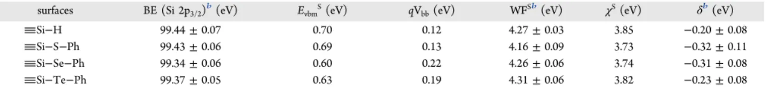
Work Function and Surface Dipoles. The effect of surface functionalization was examined for the series, Si−S− Ph, Si−Se−Ph, and Si−Te−Ph, since these groups contain the same consistent phenyl termination. Functionalization of the silicon surface can alter its electronics, resulting from band bending due to charged surface states and surface dipoles,4,83,84 and thus we wished to examine the effect of the series of chalcogenide linkers on the properties of the silicon, since earlier predictions had suggested large effects.21−23XPS can be used to determine the band bending, and work function can be obtained from UPS measurements.4,6,12,14 Measurements required multiple samples to account for measurement variability, as well as the use of gold-on-silicon as the reference for XPS, as outlined by Lewis and co-workers.4 Figure S6a,b shows the XPS spectra and cross-sectional SEM image of the Au reference used for binding energy calibration. Since the interfacial dipoles depend upon the doping level,11moderately doped n-type Si(111) was chosen since it would be expected to have the greatest range of Si 2p3/2 values depending upon
surface functionality.4
Average values of electronic properties measured for the functionalized silicon surfaces are listed inTable 2. Raw data without normalization of all measurements including XPS and secondary electron He I UPS are shown inFigures S7 and S8, as well as calculations. The data for the Si−E−Ph-terminated surfaces, as reported in Table 2, are similar to that of the
starting Si−H-terminated surface. Figure S9 depicts the energy band diagram of Si 2p3/2 binding energy with upward
band bending, corresponding to the measured band bending values. The measured work function of the Si−H-terminated surface is 4.27 ± 0.03 eV, which is similar to that reported earlier, 4.29 eV, for hydride-terminated Si(111) of the same doping.4 Upon functionalization with the phenyl chalcogenide moiety, the work functions were relatively unchanged, in the range of 4.16 ± 0.09 eV for Si−S−Ph, to 4.31 ± 0.06 for Si−Te−Ph. Other electronic characteristics, including sur-face electron affinity (χS) and surface dipole (δ), are also largely unchanged compared to the starting Si−H interface. A Si−CH3-terminated Si(111) surface with similar (moderate
n-type) doping, with full substitution of all Si−H groups enabled by the small size of the methyl group, caused only a small drop of the work function to 4.04 eV.4 A large shift of work function compared to starting Si−H was, however, observed upon substitution of hydrides with bromine atoms, Si−Br, to 4.86 eV.4 Thus, the chalcogenide terminations, which do not have the large dipole of the bromide termination and are more akin to the methyl termination in terms of electronegativity and surface dipole, do not induce much change. The small effect of Si−E−Ph-termination may also result from the low substitution levels (∼15%);1,85−88 the electronics of the silicon are thus dominated by the majority Si−H termination.
Figure 6. “Photolysis−diffusion−abstraction−addition” mechanism leads to the Si−ER bond formation. (a) Photolysis of REER molecules near the top of the organic layer results in RE• radicals. Because this film has been melted, and is thus a liquid, these radicals can diffuse throughout the film and can abstract a hydrogen from a surface Si−H bond, leading to Si• radicals. (b) Addition of REER molecules to surface Si• radicals via SH2 addition leads to Si−E bond formation. (c) Direct combination of a Si• radical with a RE• radical can also yield Si−ER bond
formation.
Table 2. Binding Energy, Work Function, and Surface Dipole of Functionalized Silicon Surfacesa
surfaces BE (Si 2p3/2)b(eV) EvbmS(eV) qVbb(eV) WFSb(eV) χS(eV) δb(eV)
Si−H 99.44 ± 0.07 0.70 0.12 4.27 ± 0.03 3.85 −0.20 ± 0.08
Si−S−Ph 99.43 ± 0.06 0.69 0.13 4.16 ± 0.09 3.73 −0.32 ± 0.11
Si−Se−Ph 99.34 ± 0.06 0.60 0.22 4.26 ± 0.06 3.74 −0.31 ± 0.08
Si−Te−Ph 99.37 ± 0.05 0.63 0.19 4.31 ± 0.06 3.82 −0.23 ± 0.08
aBE (Si 2p
3/2) is the binding energy of the Si 2p3/2peak at the surface as measured by XPS. EVBMS is the energy difference from the valence band to
Fermi level at the surface. Band bending energy is represented as qVbb. WFSis the dark work function at the silicon surface measured in the dark by
UPS. χSand δ represent surface electron affinity and the surface dipole, respectively.bBinding energy, work function, and surface dipole are displayed
as “average ± standard deviation”. The standard deviations of EVBMS and qVbbhave the same values as the ones of BE (Si 2p3/2), and the standard
deviations of χShave the same values as the ones of δ. Four identical samples were prepared for each type of silicon surface. For each sample, two
spots were measured by XPS as well as UPS, leading to each functionalization of silicon surfaces containing eight measurements. A gold-on-silicon sample was used as the reference for XPS.
■
CONCLUSIONSA straightforward approach to form Si−E−R (E = S, Se, Te) functionalities on Si(111)−H surfaces has been described using UV irradiation and gentle thermal heating with synthetically practical dialkyl/diaryl chalcogenide precursors. The mecha-nism of reactivity of the dichalcogenides appears to be radical in nature and is closely related to observed reactivity in silane molecules. The substitution level of the phenyl chalcogenide derivatives, Si−E−Ph, was lower than that of the aliphatic chalcogenide (Si−S−n-octadecyl) group, most likely due to the fact that the phenyl group obscures neighboring silicon− hydride bonds and thus sterically prevents them from reacting. Use of larger flat aromatic precursors with dichalcogenide linkages could enable access to interesting interfaces that have few linker atoms to the surface of the silicon that shield the silicon surface with potentially electronically active moieties. Higher substitution levels will need to be achieved through use of less bulky dialkyl dichalcogenide groups in order to better study the effects of Si−E bonds on the electronics of silicon.
■
ASSOCIATED CONTENT*
S Supporting InformationThe Supporting Information is available free of charge on the ACS Publications websiteat DOI:10.1021/acs.jpcc.8b00910.
Estimation of light absorption by molecules; reaction apparatus; XPS spectra for reactions under thermal conditions; water contact angle images; XPS data and water contact angle data and their representative values from the literature; representative bond angles from the literature; UV absorption spectra for diphenyl and dialkyl dichalcogenides; XPS spectrum and SEM image for Au reference; substitution level calculations; XPS spectra of Si 2p peaks and UPS spectra of all Si(111) surfaces; silicon energy levels calculation (PDF)
Movie of time series visualization of a stochastic simulation of Si−E−Ph groups packing the Si(111) surface(AVI)
■
AUTHOR INFORMATION Corresponding Author *E-mail: jburiak@ualberta.ca. ORCID Minjia Hu:0000-0002-1140-9907 Tate C. Hauger:0000-0001-5093-8302 Erik J. Luber: 0000-0003-1623-0102 Jillian M. Buriak: 0000-0002-9567-4328 NotesThe authors declare no competing financial interest.
■
ACKNOWLEDGMENTSThis work was supported by grants from the Natural Sciences and Engineering Research Council (NSERC) (grant numbers RGPIN-283291-09 and RGPIN-2014−05195), Alberta Inno-vates Technology Futures (fellowships to M.H., and grant number AITF iCORE IC50-T1 G2013000198), and the Canada Research Chairs Program (CRC 207142). We would also like to thank Drs. Anqiang He and Shihong Xu from University of Alberta NanoFAB for assistance with XPS and UPS.
■
REFERENCES(1) Plymale, N. T.; Ramachandran, A. A.; Lim, A.; Brunschwig, B. S.; Lewis, N. S. Control of the Band-Edge Positions of Crystalline Si(111) by Surface Functionalization with 3,4,5-Trifluorophenylacetylenyl Moieties. J. Phys. Chem. C 2016, 120, 14157−14169.
(2) Walter, M. G.; Warren, E. L.; McKone, J. R.; Boettcher, S. W.; Mi, Q.; Santori, E. A.; Lewis, N. S. Solar Water Splitting Cells. Chem. Rev. 2010, 110, 6446−6473.
(3) Bruce, J. P.; Oliver, D. R.; Lewis, N. S.; Freund, M. S. Electrical Characteristics of the Junction between PEDOT:PSS and Thiophene-Functionalized Silicon Microwires. ACS Appl. Mater. Interfaces 2015, 7, 27160−27166.
(4) Gleason-Rohrer, D. C.; Brunschwig, B. S.; Lewis, N. S. Measurement of the Band Bending and Surface Dipole at Chemically Functionalized Si(111)/Vacuum Interfaces. J. Phys. Chem. C 2013,
117, 18031−18042.
(5) Zhang, Z.; Yates, J. T. Band Bending in Semiconductors: Chemical and Physical Consequences at Surfaces and Interfaces. Chem.
Rev. 2012, 112, 5520−5551.
(6) Pluchery, O.; Zhang, Y.; Benbalagh, R.; Caillard, L.; Gallet, J. J.; Bournel, F.; Lamic-Humblot, A.-F.; Salmeron, M.; Chabal, Y. J.; Rochet, F. Static and Dynamic Electronic Characterization of Organic Monolayers Grafted on a Silicon Surface. Phys. Chem. Chem. Phys. 2016, 18, 3675−3684.
(7) Hu, S.; Richter, M. H.; Lichterman, M. F.; Beardslee, J.; Mayer, T.; Brunschwig, B. S.; Lewis, N. S. Electrical, Photoelectrochemical, and Photoelectron Spectroscopic Investigation of the Interfacial Transport and Energetics of Amorphous TiO2/Si Heterojunctions. J. Phys. Chem. C 2016, 120, 3117−3129.
(8) Schmidt, V.; Wittemann, J. V.; Senz, S.; Gösele, U. Silicon Nanowires: A Review on Aspects of their Growth and their Electrical Properties. Adv. Mater. 2009, 21, 2681−2702.
(9) Smaali, K.; Guérin, D.; Passi, V.; Ordronneau, L.; Carella, A.; Mélin, T.; Dubois, E.; Vuillaume, D.; Simonato, J. P.; Lenfant, S. Physical Study by Surface Characterizations of Sarin Sensor on the Basis of Chemically Functionalized Silicon Nanoribbon Field Effect Transistor. J. Phys. Chem. C 2016, 120, 11180−11191.
(10) Bashouti, M. Y.; Pietsch, M.; Brönstrup, G.; Sivakov, V.; Ristein, J.; Christiansen, S. Heterojunction Based Hybrid Silicon Nanowire Solar Cell: Surface Termination, Photoelectron and Photoemission Spectroscopy Study. Prog. Photovoltaics 2014, 22, 1050−1061.
(11) Yaffe, O.; Pujari, S.; Sinai, O.; Vilan, A.; Zuilhof, H.; Kahn, A.; Kronik, L.; Cohen, H.; Cahen, D. Effect of Doping Density on the Charge Rearrangement and Interface Dipole at the Molecule−Silicon Interface. J. Phys. Chem. C 2013, 117, 22422−22427.
(12) Urrabazo, D.; Overzet, L. J. The Effects of the Fermi Level on Ion Induced Electron Emission from Chemically and Sputter Cleaned Semiconductors. J. Phys. D: Appl. Phys. 2015, 48, 345203.
(13) Vilan, A.; Cahen, D. Chemical Modification of Semiconductor Surfaces for Molecular Electronics. Chem. Rev. 2017, 117, 4624−4666. (14) Hacker, C. A. Modifying Electronic Properties at the Silicon− Molecule Interface Using Atomic Tethers. Solid-State Electron. 2010,
54, 1657−1664.
(15) Rakshit, T.; Liang, G.-C.; Ghosh, A. W.; Datta, S. Silicon-Based Molecular Electronics. Nano Lett. 2004, 4, 1803−1807.
(16) Buriak, J. M. Organometallic Chemistry on Silicon and Germanium Surfaces. Chem. Rev. 2002, 102, 1271−1308.
(17) Maldonado, S.; Plass, K. E.; Knapp, D.; Lewis, N. S. Electrical Properties of Junctions between Hg and Si(111) Surfaces Function-alized with Short-Chain Alkyls. J. Phys. Chem. C 2007, 111, 17690− 17699.
(18) Pujari, S. P.; van Andel, E.; Yaffe, O.; Cahen, D.; Weidner, T.; van Rijn, C. J. M.; Zuilhof, H. Mono-Fluorinated Alkyne-Derived SAMs on Oxide-Free Si(111) Surfaces: Preparation, Characterization and Tuning of the Si Workfunction. Langmuir 2013, 29, 570−580.
(19) Takeuchi, N.; Kanai, Y.; Selloni, A. Surface Reaction of Alkynes and Alkenes with H-Si(111): A Density Functional Theory Study. J.
(20) Pluchery, O.; Caillard, L.; Dollfus, P.; Chabal, Y. J. Gold Nanoparticles on Functionalized Silicon Substrate under Coulomb Blockade Regime: An Experimental and Theoretical Investigation. J.
Phys. Chem. B 2018, 122, 897−903.
(21) Arefi, H. H.; Nolan, M.; Fagas, G. Role of the Head and/or Tail Groups of Adsorbed − [Xhead group]−Alkyl−[Xtail group] [X = O(H),
S(H), NH(2)] Chains in Controlling the Work Function of the
Functionalized H:Si(111) Surface. J. Phys. Chem. C 2015, 119, 11588− 11597.
(22) Arefi, H. H.; Nolan, M.; Fagas, G. Binary Functionalization of H:Si(111) Surfaces by Alkyl Monolayers with Different Linker Atoms Enhances Monolayer Stability and Packing. Phys. Chem. Chem. Phys. 2016, 18, 12952−12963.
(23) Arefi, H. H.; Fagas, G. Chemical Trends in the Work Function of Modified Si(111) Surfaces: A DFT Study. J. Phys. Chem. C 2014,
118, 14346−14354.
(24) Coulter, S. K.; Schwartz, M. P.; Hamers, R. J. Sulfur Atoms as Tethers for Selective Attachment of Aromatic Molecules to Silicon(001) Surfaces. J. Phys. Chem. B 2001, 105, 3079−3087.
(25) Yu, L. H.; Gergel-Hackett, N.; Zangmeister, C. D.; Hacker, C. A.; Richter, C. A.; Kushmerick, J. G. Molecule-Induced Interface States Dominate Charge Transport in Si−alkyl−metal Junctions. J. Phys.:
Condens. Matter 2008, 20, 374114.
(26) Lou, J. L.; Shiu, H. W.; Chang, L. Y.; Wu, C. P.; Soo, Y.-L.; Chen, C.-H. Preparation and Characterization of an Ordered 1-Dodecanethiol Monolayer on Bare Si(111) Surface. Langmuir 2011,
27, 3436−3441.
(27) Huang, Y.-S.; Chen, C.-H.; Chen, C.-H.; Hung, W.-H. Fabrication of Octadecyl and Octadecanethiolate Self-Assembled Monolayers on Oxide-Free Si(111) with a One-Cell Process. ACS
Appl. Mater. Interfaces 2013, 5, 5771−5776.
(28) Sano, H.; Ohno, K.; Ichii, T.; Murase, K.; Sugimura, H. Alkanethiol Self-Assembled Monolayers Formed on Silicon Substrates.
Jpn. J. Appl. Phys. 2010, 49, 01AE09.
(29) Bhartia, B.; Puniredd, S. R.; Jayaraman, S.; Gandhimathi, C.; Sharma, M.; Kuo, Y.-C.; Chen, C.-H.; Reddy, V. J.; Troadec, C.; Srinivasan, M. P. Highly Stable Bonding of Thiol Monolayers to Hydrogen-Terminated Si via Supercritical Carbon Dioxide: Toward a Super Hydrophobic and Bioresistant Surface. ACS Appl. Mater.
Interfaces 2016, 8, 24933−24945.
(30) Yasseri, A. A.; Syomin, D.; Loewe, R. S.; Lindsey, J. S.; Zaera, F.; Bocian, D. F. Structural and Electron-Transfer Characteristics of O-, S-, and Se-Tethered Porphyrin Monolayers on Si(100). J. Am. Chem.
Soc. 2004, 126, 15603−15612.
(31) Balakumar, A.; Lysenko, A. B.; Carcel, C.; Malinovskii, V. L.; Gryko, D. T.; Schweikart, K.-H.; Loewe, R. S.; Yasseri, A. A.; Liu, Z.; Bocian, D. F.; Lindey, J. S. Diverse Redox-Active Molecules Bearing O-, S-, or Se-Terminated Tethers for Attachment to Silicon in Studies of Molecular Information Storage. J. Org. Chem. 2004, 69, 1435−1443. (32) Hu, M.; Liu, F.; Buriak, J. M. Expanding the Repertoire of Molecular Linkages to Silicon: Si−S, Si−Se, and Si−Te Bonds. ACS
Appl. Mater. Interfaces 2016, 8, 11091−11099.
(33) Buriak, J. M.; Sikder, M. D. H. From Molecules to Surfaces: Radical-Based Mechanisms of Si−S and Si−Se Bond Formation on Silicon. J. Am. Chem. Soc. 2015, 137, 9730−9738.
(34) Nemanick, E. J.; Hurley, P. T.; Webb, L. J.; Knapp, D. W.; Michalak, D. J.; Brunschwig, B. S.; Lewis, N. S. Chemical and Electrical Passivation of Single-Crystal Silicon(100) Surfaces through a Two-Step Chlorination/Alkylation Process. J. Phys. Chem. B 2006, 110, 14770−14778.
(35) Bahl, M. K.; Watson, R. L.; Irgolic, K. J. X-ray Photoemission Studies of Tellurium and Some of Its Compounds. J. Chem. Phys. 1977, 66, 5526−5535.
(36) Chu, J. Y. C.; Lewicki, J. W. Thermal Decomposition of Bis(diphenylmethyl) Diselenide. J. Org. Chem. 1977, 42, 2491−2493. (37) Chaudhury, M. K.; Whitesides, G. M. Correlation Between Surface Free Energy and Surface Constitution. Science 1992, 255, 1230−1232.
(38) Bain, C. D.; Whitesides, G. M. Molecular-Level Control over Surface Order in Self-Assembled Monolayer Films of Thiols on Gold.
Science 1988, 240, 62−63.
(39) Biebuyck, H. A.; Bain, C. D.; Whitesides, G. M. Comparison of Organic Monolayers on Polycrystalline Gold Spontaneously As-sembled from Solutions Containing Dialkyl Disulfides or Alkanethiols.
Langmuir 1994, 10, 1825−1831.
(40) Huck, L. A.; Buriak, J. M. UV-Initiated Hydrosilylation on Hydrogen-Terminated Silicon (111): Rate Coefficient Increase of Two Orders of Magnitude in the Presence of Aromatic Electron Acceptors. Langmuir 2012, 28, 16285−16293.
(41) Bain, C. D.; Evall, J.; Whitesides, G. M. Formation of Monolayers by the Coadsorption of Thiols on Gold: Variation in the Head Group, Tail Group, and Solvent. J. Am. Chem. Soc. 1989,
111, 7155−7164.
(42) Liu, Y.; Shen, L. From Langmuir Kinetics to First- and Second-Order Rate Equations for Adsorption. Langmuir 2008, 24, 11625− 11630.
(43) Escorihuela, J.; Zuilhof, H. Rapid Surface Functionalization of Hydrogen-Terminated Silicon by Alkyl Silanols. J. Am. Chem. Soc. 2017, 139, 5870−5876.
(44) Sieval, A. B.; Opitz, R.; Maas, H. P. A.; Schoeman, M. G.; Meijer, G.; Vergeldt, F. J.; Zuilhof, H.; Sudhölter, E. J. R. Monolayers of 1-Alkynes on the H-Terminated Si(100) Surface. Langmuir 2000,
16, 10359−10368.
(45) Sieval, A. B.; Demirel, A. L.; Nissink, J. W. M.; Linford, M. R.; van der Maas, J. H.; de Jeu, W. H.; Zuilhof, H.; Sudhölter, E. J. R. Highly Stable Si−C Linked Functionalized Monolayers on the Silicon (100) Surface. Langmuir 1998, 14, 1759−1768.
(46) Lenfant, S.; Guerin, D.; Tran Van, F.; Chevrot, C.; Palacin, S.; Bourgoin, J. P.; Bouloussa, O.; Rondelez, F.; Vuillaume, D. Electron Transport through Rectifying Self-Assembled Monolayer Diodes on Silicon: Fermi-Level Pinning at the Molecule−Metal Interface. J. Phys.
Chem. B 2006, 110, 13947−13958.
(47) Srivastava, P.; Chapman, W. G.; Laibinis, P. E. Odd−Even Variations in the Wettability of n-Alkanethiolate Monolayers on Gold by Water and Hexadecane: A Molecular Dynamics Simulation Study.
Langmuir 2005, 21, 12171−12178.
(48) Ulman, A. Self-Assembled Monolayers of Alkyltrichiorosilanes: Building Blocks for Future Organic Materials. Adv. Mater. 1990, 2, 573−582.
(49) Wang, D.; Buriak, J. M. Electrochemically Driven Organic Monolayer Formation on Silicon Surfaces Using Alkylammonium and Alkylphosphonium Reagents. Surf. Sci. 2005, 590, 154−161.
(50) Li, Y.-H.; Buriak, J. M. Dehydrogenative Silane Coupling on Silicon Surfaces via Early Transition Metal Catalysis. Inorg. Chem. 2006, 45, 1096−1102.
(51) Leroux, Y. R.; Fei, H.; Noël, J.-M.; Roux, C.; Hapiot, P. Efficient Covalent Modification of a Carbon Surface: Use of a Silyl Protecting Group to Form an Active Monolayer. J. Am. Chem. Soc. 2010, 132, 14039−14041.
(52) Anariba, F.; DuVall, S. H.; McCreery, R. L. Mono- and Multilayer Formation by Diazonium Reduction on Carbon Surfaces Monitored with Atomic Force Microscopy “Scratching. Anal. Chem. 2003, 75, 3837−3844.
(53) Marynowski, W.; Klucznik, T.; Baranowska, K.; Dołęga, A.; Wojnowski, W. Tri(mesityloxy)silanethiol − The First Structurally Characterized Organoxysilanethiol (Contributions to the Chemistry of Silicon−Sulfur Compounds. 77 [1]). Z. Anorg. Allg. Chem. 2010, 636, 685−687.
(54) Herman, A.; Godlewska, S.; Ponikiewski, Ł.; Kruczyński, T.; Dołȩga, A. Propeller-Like Chirality of Methyl-Tris (2,6-diisopropylphenoxy)Silylsulfide. Silicon 2016, 8, 105−110.
(55) Li, S. L.; Truhlar, D. G. Full-Dimensional Ground- and Excited-State Potential Energy Surfaces and Excited-State Couplings for Photo-dissociation of Thioanisole. J. Chem. Phys. 2017, 146, 064301.
(56) Schweig, A.; Thon, N. Measurement of Relative Conformational Stabilities by Variable Temperature Photoelectron Spectroscopy. A
Study of Rotational Isomerism in Thioanisole. Chem. Phys. Lett. 1976,
38, 482−485.
(57) Bandoli, G.; Clemente, D. A.; Tondello, E.; Dondoni, A. Crystal, Molecular, and Electronic Structure of 4-Dimethylaminophenyl Phenyl Sulphide. J. Chem. Soc., Perkin Trans. 2 1974, 157−160.
(58) Hamed, E. A.; El-Bardan, A. A.; Saad, E. F.; Gohar, G. A.; Hassan, G. M. Nucleophilic Substitutions at the Pyridine Ring. Conformational Preference of the Products and Kinetics of the Reactions of 2-Chloro-3-Nitro- and 2-Chloro-5-Nitro-Pyridines with Arenethiolates†. J. Chem. Soc., Perkin Trans. 2 1997, 2415−2422.
(59) van der Heijden, S. P. N.; Chandler, W. D.; Robertson, B. E. Conformations of Bridged Diphenyls. IX. Crystal Structure of 2-(4′-Carbomethoxy-2′-nitrothiophenyl)-1,3,5-trimethylbenzene. Can. J.
Chem. 1975, 53, 2102−2107.
(60) Bzhezovskii, V. M.; Kapustin, E. G. Steric and Electronic Structure of Selenoanisole: A Quantum-Chemical Study. Russ. J. Gen.
Chem. 2003, 73, 54−60.
(61) Fujihara, H.; Mima, H.; Ikemori, M.; Furukawa, N. New Hypervalent σ-Selenanes with a Transannular Se-N Bond from N-Methyl-5H,7H-Dibenzo[b,g][1,5]Selenazocine. J. Am. Chem. Soc. 1991, 113, 6337−6338.
(62) Frisell, H.; Engman, L. Molecular Modelling of Some para-Substituted Aryl Methyl Telluride and Diaryl Telluride Antioxidants. J.
Mol. Struct. 2000, 526, 103−114.
(63) Harada, Y.; Koitaya, T.; Mukai, K.; Yoshimoto, S.; Yoshinobu, J. Spectroscopic Characterization and Transport Properties of Aromatic Monolayers Covalently Attached to Si(111) Surfaces. J. Phys. Chem. C 2013, 117, 7497−7505.
(64) Wallart, X.; Henry de Villeneuve, C.; Allongue, P. Truly Quantitative XPS Characterization of Organic Monolayers on Silicon: Study of Alkyl and Alkoxy Monolayers on H−Si(111). J. Am. Chem.
Soc. 2005, 127, 7871−7878.
(65) Plymale, N. T.; Kim, Y.-G.; Soriaga, M. P.; Brunschwig, B. S.; Lewis, N. S. Synthesis, Characterization, and Reactivity of Ethynyl- and Propynyl-Terminated Si(111) Surfaces. J. Phys. Chem. C 2015, 119, 19847−19862.
(66) Scheres, L.; Giesbers, M.; Zuilhof, H. Organic Monolayers onto Oxide-Free Silicon with Improved Surface Coverage: Alkynes versus Alkenes. Langmuir 2010, 26, 4790−4795.
(67) Cicero, R. L.; Linford, M. R.; Chidsey, C. E. D. Photoreactivity of Unsaturated Compounds with Hydrogen-Terminated Silicon(111).
Langmuir 2000, 16, 5688−5695.
(68) Sieval, A. B.; van den Hout, B.; Zuilhof, H.; Sudhölter, E. J. R. Molecular Modeling of Covalently Attached Alkyl Monolayers on the Hydrogen-Terminated Si(111) Surface. Langmuir 2001, 17, 2172− 2181.
(69) Yuan, S.-L.; Cai, Z.-T.; Jiang, Y.-S. Molecular Simulation Study of Alkyl Monolayers on the Si(111) Surface. New J. Chem. 2003, 27, 626−633.
(70) Sieval, A. B.; van den Hout, B.; Zuilhof, H.; Sudhölter, E. J. R. Molecular Modeling of Alkyl Monolayers on the Si(111) Surface.
Langmuir 2000, 16, 2987−2990.
(71) Ballestri, M.; Chatgilialoglu, C.; Clark, K. B.; Griller, D.; Giese, B.; Kopping, B. Tris(trimethylsilyl)silane as a Radical-Based Reducing Agent in Synthesis. J. Org. Chem. 1991, 56, 678−683.
(72) Chatgilialoglu, C. Structural and Chemical Properties of Silyl Radicals. Chem. Rev. 1995, 95, 1229−1251.
(73) Linford, M. R.; Fenter, P.; Eisenberger, P. M.; Chidsey, C. E. D. Alkyl Monolayers on Silicon Prepared from 1-Alkenes and Hydrogen-Terminated Silicon. J. Am. Chem. Soc. 1995, 117, 3145−3155.
(74) Sieval, A. B.; Vleeming, V.; Zuilhof, H.; Sudhölter, E. J. R. An Improved Method for the Preparation of Organic Monolayers of 1-Alkenes on Hydrogen-Terminated Silicon Surfaces. Langmuir 1999,
15, 8288−8291.
(75) Soundararajan, N.; Jackson, J. E.; Platz, M. S. Reaction of Triethylsilyl Radical with Sulfides, a Laser Flash Photolysis Study. J.
Phys. Org. Chem. 1988, 1, 39−46.
(76) McDonough, J. E.; Weir, J. J.; Carlson, M. J.; Hoff, C. D.; Kryatova, O. P.; Rybak-Akimova, E. V.; Clough, C. R.; Cummins, C. C.
Solution Calorimetric and Stopped-Flow Kinetic Studies of the Reaction of •Cr(CO)3C5Me5 with PhSe−SePh and PhTe−TePh.
Experimental and Theoretical Estimates of the Se−Se, Te−Te, H−Se, and H−Te Bond Strengths. Inorg. Chem. 2005, 44, 3127−3136.
(77) McDonough, J. E.; Weir, J. J.; Sukcharoenphon, K.; Hoff, C. D.; Kryatova, O. P.; Rybak-Akimova, E. V.; Scott, B. L.; Kubas, G. J.; Mendiratta, A.; Cummins, C. C. Comparison of Thermodynamic and Kinetic Aspects of Oxidative Addition of PhE−EPh (E = S, Se, Te) to Mo(CO)3(PR3)2, W(CO)3(PR3)2, and Mo(N[tBu]Ar)3 Complexes.
The Role of Oxidation State and Ancillary Ligands in Metal Complex Induced Chalcogenyl Radical Generation. J. Am. Chem. Soc. 2006, 128, 10295−10303.
(78) Walsh, R. Bond Dissociation Energy Values in Silicon-Containing Compounds and Some of Their Implications. Acc. Chem.
Res. 1981, 14, 246−252.
(79) Stewart, M. P.; Buriak, J. M. Photopatterned Hydrosilylation on Porous Silicon. Angew. Chem., Int. Ed. 1998, 37, 3257−3260.
(80) Terry, J.; Mo, R.; Wigren, C.; Cao, R.; Mount, G.; Pianetta, P.; Linford, M. R.; Chidsey, C. E. D. Reactivity of the H-Si (111) Surface.
Nucl. Instrum. Methods Phys. Res., Sect. B 1997, 133, 94−101.
(81) Terry, J.; Linford, M. R.; Wigren, C.; Cao, R.; Pianetta, P.; Chidsey, C. E. D. Determination of the Bonding of Alkyl Monolayers to the Si(111) Surface Using Chemical-Shift, Scanned-Energy Photoelectron Diffraction. Appl. Phys. Lett. 1997, 71, 1056−1058.
(82) Zavitsas, A. A.; Chatgilialoglu, C. Energies of Activation. The Paradigm of Hydrogen Abstractions by Radicals. J. Am. Chem. Soc. 1995, 117, 10645−10654.
(83) Liu, F.; Hauger, T. C.; Olsen, B. C.; Luber, E. J.; Buriak, J. M. Polymers, Plasmons, and Patterns: Mechanism of Plasmon-Induced Hydrosilylation on Silicon. Chem. Mater. 2016, 28, 9158−9168.
(84) Giesbrecht, P. K.; Bruce, J. P.; Freund, M. S. Electric and Photoelectric Properties of 3,4−Ethylenedioxythiophene-Function-alized n-Si/PEDOT:PSS Junctions. ChemSusChem 2016, 9, 109−117. (85) Garner, L. E.; Steirer, K. X.; Young, J. L.; Anderson, N. C.; Miller, E. M.; Tinkham, J. S.; Deutsch, T. G.; Sellinger, A.; Turner, J. A.; Neale, N. R. Covalent Surface Modification of Gallium Arsenide Photocathodes for Water Splitting in Highly Acidic Electrolyte.
ChemSusChem 2017, 10, 767−773.
(86) MacLeod, B. A.; Steirer, K. X.; Young, J. L.; Koldemir, U.; Sellinger, A.; Turner, J. A.; Deutsch, T. G.; Olson, D. C. Phosphonic Acid Modification of GaInP2 Photocathodes Toward Unbiased
Photoelectrochemical Water Splitting. ACS Appl. Mater. Interfaces 2015, 7, 11346−11350.
(87) Rangan, S.; Batarseh, A.; Chitre, K. P.; Kopecky, A.; Galoppini, E.; Bartynski, R. A. Tuning Energy Level Alignment at Organic/ Semiconductor Interfaces Using a Built-In Dipole in Chromophore− Bridge−Anchor Compounds. J. Phys. Chem. C 2014, 118, 12923− 12928.
(88) Li, Y.; O’Leary, L. E.; Lewis, N. S.; Galli, G. Combined Theoretical and Experimental Study of Band-Edge Control of Si through Surface Functionalization. J. Phys. Chem. C 2013, 117, 5188− 5194.