HAL Id: hal-02940841
https://hal.archives-ouvertes.fr/hal-02940841
Submitted on 23 Sep 2020
HAL is a multi-disciplinary open access archive for the deposit and dissemination of sci-entific research documents, whether they are pub-lished or not. The documents may come from teaching and research institutions in France or abroad, or from public or private research centers.
L’archive ouverte pluridisciplinaire HAL, est destinée au dépôt et à la diffusion de documents scientifiques de niveau recherche, publiés ou non, émanant des établissements d’enseignement et de recherche français ou étrangers, des laboratoires publics ou privés.
Frank partial dislocation in Ti2AlC-MAX phase induced
by matrix-Cu diffusion
Wenbo Yu, Julien Guénolé, Jaafar Ghanbaja, Maxime Vallet, Antoine Guitton
To cite this version:
Wenbo Yu, Julien Guénolé, Jaafar Ghanbaja, Maxime Vallet, Antoine Guitton. Frank partial disloca-tion in Ti2AlC-MAX phase induced by matrix-Cu diffusion. Scripta Materialia, Elsevier, 2021, 191, pp.34-39. �10.1016/j.scriptamat.2020.09.007�. �hal-02940841�
1
Frank partial dislocation in Ti
2AlC-MAX phase
induced by matrix-Cu diffusion
Wenbo YU a, Julien GUÉNOLÉ b,c, Jaafar GHANBAJA d, Maxime VALLET e,
Antoine GUITTON b,c,*
a Center of Materials Science and Engineering, School of Mechanical and Electronic Control
Engineering, Beijing Jiaotong University, Beijing, China.
b Université de Lorraine – CNRS – Arts et Métiers ParisTech – LEM3, Metz, France.
c Laboratory of Excellence on Design of Alloy Metals for low-mAss Structures (DAMAS),
Université de Lorraine, Metz, France.
d Université de Lorraine – CNRS – IJL, Nancy, France.
e CEA, DEN, Service de Recherches de Métallurgie Physique, Université Paris-Saclay,
Gif-sur-Yvette, France.
* Corresponding author: Université de Lorraine – CNRS – Arts et Métiers ParisTech – LEM3, 7 rue Félix Savart, 57070 Metz, France; mail: antoine.guitton@univ-lorraine.fr; phone: +33 372 747 787.
Abstract
The control of complex nanostructures is one of the most promising strategy for designing tailored property materials. Ti2AlC, as nanolayered
ternary materials combining both ceramics and metals properties, could efficiently reinforce metal matrix composite by its decomposition into nano-Ti2C particles. However, the comprehensive description of the diffusion
mechanisms of Cu element into Ti2AlC during its decomposition has not
yet been revealed. Herein, we report detailed characterizations of Cu and Ti2AlC interlayers by means of high-resolution electron microscopy and
atomic-scale simulations. In particular, we report the formation of Ti2AlxCuyC solid solutions. Furthermore, we demonstrate the formation of
Ti2C platelets and evidenced Frank partial dislocations that are not
expected to be found in such material. Impacts of such defects are discussed in the framework of mechanical behavior.
Keywords: Ti2AlC, Cu, composite, diffusion, High-Resolution TEM, EELS,
2
The design of new materials is one of the main scientific challenges in order to support new technologies that follow the fast evolutions of our society. In this context, structurally complex nanolayered materials such as MAX phases were developed over the last 30 years.
Mn+1AXn phases (where n = 1 to 3, M is a transition metal, A is an A-group
element and X is nitrogen or carbon [1]) have remarkable properties such as low density, high modulus, self-lubrication properties and unique mechanical behaviors both at room and high temperatures [2] [3] [4] [5] [6] [7]. As an example, the easy out-diffusion of A-elements is a key property of MAX phases at high temperature. It is essentially due to their decomposition [8]. On the one hand, it favors the formation of well-bonded interfaces between phases, and on the other hand, it endows MAX phases a good self-healing capacity and exceptional oxidation resistance. The primitive cell of MAX phases is hexagonal and described as a stacking of n M6X octahedron layers with one layer of A-element.
Measurements of lattice parameters with numerous methods reveal that MAX phases exhibit high crystalline anisotropy with a ac ratio generally higher than 4. This class of nanolayered materials made from low-cost elements uniquely combines properties of both ceramics (refractory, high stiffness, low density – 4.5 g cm-3 for Ti3SiC2 –, low ductility at room temperature) and metals (high thermal
and electric conductivity, thermal shocks resistance, low hardness, mechanical resistance). With this remarkable set of properties, MAX phases open new research tracks, in particular on materials for hydrogen storage [9] and two-dimensional materials (MXenes) [10] [11].
As a response to the increasing demand for new materials, tailored property composites are highly promising. Copper is one of the most used metals essentially because of its very high electrical conductivity. However, its low strength and its low wear resistance properties result in premature failure of components, thus restricting its wide range of applications, particularly in homopolar machines and in overhead current lines for railway. One possible route among others for overtaking these obstacles is to reinforce the Cu matrix by the introduction of a layered ternary MAX phases, such asTi2SnC or Ti2AlC
[12] [13] [14].
In the framework of MAX-Cu composites, Ti-based MAX phases including Ti3AlC2, Ti2AlC and Ti2AlN have been adopted [15]. Zhang et al. suggested that
the de-intercalation of Al along basal planes induces the formation of TixC
platelets in Ti3AlC2-reinforced Cu composites [8]. The solid solution (Ti 1-εCuε)3(Al,Cu)C2 has been reported in sintered Ti3AlC2-Cu powders in which the
presence of Cu is mainly located on the Al sites of the MAX phases [16] [17] [18]. These studies emphasize that the diffusion mechanisms between Ti-based MAX phases and Cu are strongly related to temperature. However, the different steps of this mechanism have never been observed yet, including formation and decomposition of Ti3AlCuC2, Ti2AlCuN or Ti2AlCuC solid solutions.
3
In order to design and tailor Cu composite reinforced by layered MAX phases, this work aims to get a comprehensive picture of structural changes caused by the diffusion of Cu in the Ti2AlC MAX phase. We report detailed
characterizations at the atomic-scale by high-resolution scanning transmission electron microscope (HR-STEM) combined with atomic electron energy-loss spectroscopy (EELS) and electron diffraction spectroscopy (EDS) of a Ti2AlC–Cu
composite. Our unique experimental observations are enlightened by atomistic simulations.
Fully dense Ti2AlC were prepared by hot isostatic pressing (HIP). Powders
of Ti (150-250 µm, 99.5% purity), Al (45-150 µm, 99.5% purity) and TiC (<45 µm, 98% purity) were mixed in stoichiometric proportions and placed into a hot isostatic press where the powder compact was heated up to 1400°C under a pressure of 80 MPa [19]. Then the polished bulk Ti2AlC was encapsulated with
pure Cu powders (99.9%, 50 µm) and it was uniaxial compressed into together under 60 MPa. Subsequently, the capsule was sintered at 700°C for 30 min under Ar atmosphere. More details on the junction between Ti2AlC and Cu are given
the supplementary materials.
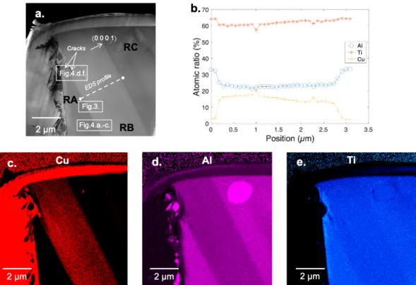
Figure 1: chemical characterization of the Cu– MAX phase composite a. HAADF-STEM micrograph at low magnification of the thin foil. Three regions labelled A (RA), B (RB) and C (RC) are distinguished. The
basal-plane direction (0 0 0 1) is also shown. Several cracks are observed in the vicinity of the Cu/Ti2AlC
junction. b. EDS line profile taken along the dot line in a. c.-e. EDS maps of Cu, Al and Ti respectively. White rectangles in a. localize where Figure 2 and Figure 3 were taken.
A thin foil was prepared near the joining interface by focused ion beam (FIB) milling with a ThermoFisher Helios Nanolab Dual Beam (see supplementary materials for exact location). Finally, HR-STEM, EDS and EELS investigations
4
were carried out using a JEOL JEM-ARM 200F Cold FEG TEM/STEM, operating at 200 kV and equipped with a spherical aberration probe and image correctors (point resolution 0.12 nm in TEM mode and 0.078 nm in STEM mode).
Figure 1.a shows a STEM micrograph in high-angle annular dark-field (HAADF) mode at low magnification. Three regions with different contrasts are
easily distinguished in the Ti2AlC area and they are respectively labelled as RA,
RB and RC (Figure 1.a.). Region RB appears as a bright band parallel to (0 0 0 1) basal planes. As HAADF detector senses a greater signal from atoms with a higher atomic number Z, causing them to appear brighter in the resulting image. The mean Z of the region RB is thus expected to be higher than in region RA and region RC. The EDS line profile on both sides of the region RB (Figure 1.b) combined with the EDS maps (Figure 1.c.-e.) confirm this observation: the atomic ratio of Al (Z=13) drops from ~33% to ~23% when crossing the boundary between regions RA and RB and it stays stable at ~23% in region RB. Then it goes back to ~33% when crossing the other boundary from RB to RC. Meanwhile the atomic ratio of Cu (Z=29) increases from ~2% to ~15% inside the region RB. Concerning Ti (Z=22), the atomic ratio remains quite stable at ~62%. Note that several cracks along basal planes are observed close to the Cu/Ti2AlC junction.
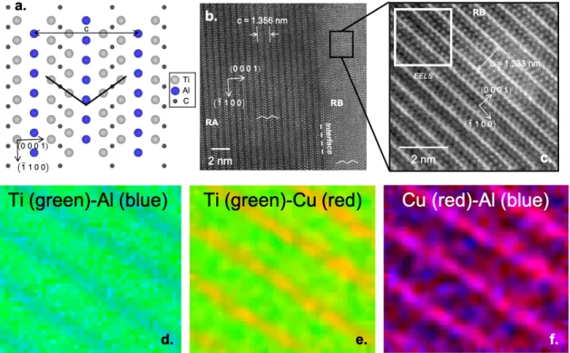
Figure 2: Atomic EELS characterization. a. Crystallographic structure of Ti2AlC projected along #1 1 2$ 0%
b.-c. HR-STEM HAADF of the interface between region A (RA) and region B (RB). The electron beam is along #1 1 2$ 0%. The white square in c. localizes the area in region B where the EELS maps were acquired (d., e. and f.). Zigzag lines in a. and b. highlight the stacking of TiC planes, characteristic of the crystallography of a 211 MAX phase family.
5
The HAADF-STEM micrographs were captured at the interface between region RA and region RB, as shown in Figure 2.b.c. The observed crystallographic lattice is consistent with the expected one of the 211-MAX phase projected along &1 1 2' 0(: zigzag stacking (Figure 2.a, black lines) of two TiC
planes followed by one Al plane, the Al plane being the axis of symmetry of the zigzag. Here again, region RB appears brighter than region RA. More precisely, the change of contrast mainly comes from A-planes that are located between two adjacent Ti planes that appear brighter. EELS maps of Figure 2.d.-f. clearly evidenced that Cu atoms replace Al in the crystallographic lattice. Combining the EDS (Figure 1) and EELS results (Figure 2), one expects that solid solutions are formed in region RA and in region RB with the average formula Ti2Al1.1Cu0.06C
and Ti2Al0.74Cu0.49C, respectively.
Figure 3: Observations of several steps of the diffusion of Cu. a.-e. HR-STEM HAADF micrographs far
(a.-c.) and in the vicinity (d.-e.) of the Cu/Ti2AlC junction. For a.-c. and f., the electron beam is along #1 1
2$ 0% while it is along #1$ 1 0 0% for d. and e. d. is a low-magnification micrograph enables to localize where
micrographs e. and f. were taken. The Cu/Ti2AlC junction is localized on the left. f. shows Ti2C platelets
(white and yellow arrows).
Figure 3 depicts some steps of the formation of Ti2C platelets. Figure
3.a.-c. first show the intercalation of Cu in A-planes along basal planes of Ti2AlC.
Yellow arrows localize bright “atomic channels” along basal planes. This change of contrast can be attributed to a localized increase of the atomic number Z due to the insertion of Cu atoms in A-planes of Ti2AlC. Figure 3.c. shows the interface
between region RA and region RB where the solid solution Ti2Al0.74Cu0.49C is
6
diffusion of Cu along basal planes. Close to the Cu source, i.e. close to the Cu/Ti2AlC junction (Figure 3.d.), A-planes de-intercalate (Figure 3.e.) forming a
partial dislocation lying in the basal plane (Figure 3.e.) with a Burgers vector clearly along [0 0 0 1]. In Figure 3.f., two sorts of Ti2C-platelets are
distinguishable: perfect connection of the adjacent Ti planes (Figure 3.f., yellow arrows) and unperfect connection (Figure 3.f., white arrows) associated with a slide of ~0.26 nm along 〈1 1& 0 0〉. This sliding direction was already reported in the case of stacking faults with an insertion of MX planes [20]. In the crystallographic point of view of Ti2C-platelets, both connections between
adjacent Ti planes in MAX phases can be seen as twin boundary (TB) and a either perfect (Figure 3.f., yellow arrows) or shifted (Figure 3.f., white arrows) [21]. Note that in the Ti2AlC point of view, they are seen as stacking faults where one
A-plane was removed. Another description leads that Ti2C platelets localized by
yellow arrows in Figure 3.f. can be seen as hexagonal Ti2C as well. The TB
description will be used in the followings.
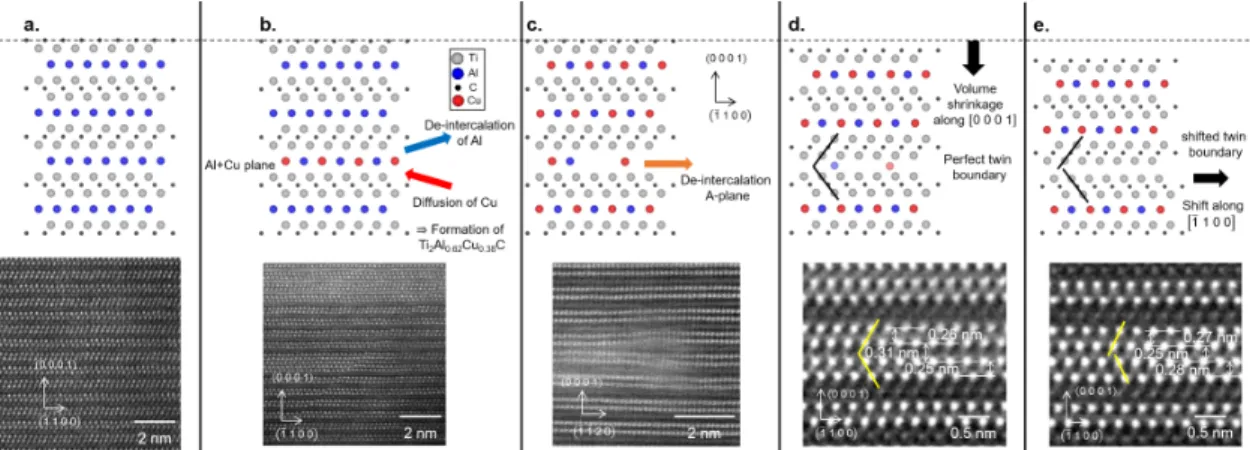
Figure 4: Molecular static simulations of a de-intercalated A-element plane. a-d sliced views of the Frank partial dislocation along the dislocation line #1$ 1 0 0% formed by the removal of an A-element half-plane, a. chemical representation: atoms in grey and blue represent Ti and A-element, respectively, b. structural representation: atoms in red, grey and green represent hexagonal bulk, dislocation core and
stacking fault structures, respectively, c. atomic elastic strain shear component (εxz), d. Burgers circuit and
Burgers vector of the Frank partial dislocation on the magnified dislocation core structure, e. critical stress required to reconstruct the perfect twin boundary into n shifted twin boundary or a disordered phase, as
function of the fraction A A* of remaining de-intercalated A-element, f stable configurations of a twin 0
boundary with A A* 0= 0.04 at zero stress and at the critical stress. The trend lines in e are guides for the
eye.
We investigated further the atomistic features that we observed by means of molecular static simulations with the open source program LAMMPS [22]. As surrogate for the Ti2AlC MAX phase for which no interatomic potential are freely
available, the Ti2Al layered phase has been chosen and modelled by a
interatomic potential developed by Kim et al. [23] based on the second nearest-neighbor modified embedded-atom method (2NN-MEAM). It consists on the
7
same structure as for the Ti2AlC MAX phase, without the layer of carbon atoms.
We observed that this configuration is stable both under pressure and temperature with the chosen potential. In this work, the Ti2Al phase is thus used
as surrogate for a structure with A-element layers that intercalates within double Ti layers. The static relaxations of the samples were performed by a succession of conjugate gradient [24] and FIRE [25] minimizations to ensure both global pressure relaxation and fast optimization of atomic positions. The atomistic samples are prepared, analyzed and visualized with Ovito [26]. The local crystallographic environment is characterized by the adaptive common neighbor analysis (CNA) method [27]. The atomic elastic strain is derived from the gradient of the elastic displacement of the atoms computed between a perfect fictious crystallographic configuration and the current deformed configuration. More details can be found in the work from Stukowski and Arsenlis [28].
Figure 4.a.-d. show the atomistic configuration of the ground state of a basal dislocation formed by the removal of an A-element half-plane. Figure 4.a. and Figure 4.b. show a sliced view of the dislocation along the dislocation line (1& 1 0 0) colored by chemical species (grey, Ti; blue, Al) and local crystallographic structure. Figure 4.b. in particular evidences the core (grey) and the stacking fault (green) of the partial dislocation. The elastic strain field generated by the dislocation is primarily directed along the Z-[0 0 0 1] direction as illustrated in Figure 4.c.: only the shear component εxz is significant while the
components εxy and εyz remain negligible. Figure 4.d. presents a magnified view
of the dislocation core structure and illustrates the Burgers circuit. In our simulation, the Burgers vector is b*⃗=c
6[0 0 0 1] with a norm measured at 2.3 Å.
Figure 4.e. shows the critical stress required to reconstruct the perfect TB into a shifted TB or a disordered phase, as function of the remaining non-diffused A-element. The diffusion of A atoms within an A-interlayer is characterized by the ratio A
A0 of the number of atoms remaining in the interlayer after diffusion (A) with
the number of atoms initially forming the interlayer (A0). The critical stress shows
a moderate increase for medium A concentration (0.0< A
A0<0.8) and a steep
increase for concentration of A close to the dense interlayer (AA
0>0.8). Note that
large concentration of A associated with very high critical stress leads to the formation of locally disordered Ti – A-element phase instead of a shifted TB. Figure 4.f. shows an example of the ground states of the TB formed after the diffusion of an A-element interlayer. In a stress-free environment, the TB exhibits a perfect structure independently on AA
0 (Figure 4.f., σ[0001]=0). As the stress
normal to the TB plane reaches the critical value, the TB becomes shifted (Figure 4.f., σ[0001]>0).
8
Figure 5: Formation of Ti2C platelets. Here the projection axis of the crystallographic structures is #1 1 2$ 0%. As illustration of each steps of the mechanism, HR-STEM pictures are zooms on interesting
areas of Figure . a. initial step: the perfect crystal of Ti2AlC. b. de-intercalation of Al and diffusion of Cu
for forming an atomic channel of Ti2Al0.62Cu0.38C solid solution. c. de-intercalation of one A plane. d.
volume shrinkage along the c-axis and formation of one Ti2C platelet. e. shift along #1$ 1 0 0% of one part
of the platelet.
Based on our experimental and numerical results, we propose a comprehensive description of the formation of Ti2C platelets, as illustrated in
Figure 5. In presence of Cu and at 700°C, Al de-intercalate along basal planes of Ti2AlC while Cu atoms diffuse progressively and replace Al atoms in the lattice
(Figure 5.a.-b.). This creates “atomic channels”. The diffusion of Cu continues until the channel is filled, thus forming the solid solution Ti2Al0.74Cu0.49C (Figure
5.b.). The interface between both areas with high and low concentration of Cu will diffuse by the successive addition of filled channels (Figure 5.c., white thick arrow). Then, atoms in A-planes de-intercalate (Figure 5.c.), thus forming a Frank partial dislocation with a Burgers vector b*⃗=c6[0 0 0 1]. The de-intercalation will propagate along (1 1 2& 0) by climbing of this c-dislocation. The nucleation of Frank partial dislocations causes a volume shrinkage along the c-axis (Figure 5.d.) i.e. the 2nd and the 3rd Ti planes move closer to each other and form a perfect
TB. Note that this volume shrinkage can lead to the initiation of cracks in (0 0 0 1) planes, as observed in Figure 1.a. To minimize the electrostatic repulsion between the adjacent Ti planes on both sides of the platelet, the perfect TB reconstructs into a perfect TB by sliding along 〈1 1& 0 0〉 (Figure 5.e.). Our simulations tend to indicate that experimentally observed shifted twin boundaries might effectively contain a low but significant concentration of A-element that cannot be visible given the limitation of the TEM resolution.
In summary, by combining atomically resolved experiments and simulations, we propose a step-by-step scenario for the diffusion of Cu in Ti2AlC MAX phase:
(i) Replacement of Al by Cu diffusion, leading to the formation atomic channels of solid solution, (ii) A-planes de-intercalation, leading to the formation of Frank partial dislocations, (iii) Volume shrinkage along the c-axis, leading to the
9
formation of perfect TB in Ti2C platelets, (iv) Minimization of the energy by a slide,
leading to the formation of shifted TB in Ti2C platelets.
The formation of the Frank partial dislocation might be of particular importance. Deformation mechanisms in MAX phases are based on dislocations [5], in particular a-type basal dislocations [3] [6] [5] [7] with the so-called mechanism of kink bands [29] [30] [31]. To date, c and a+c dislocations have been considered as impossible dislocation type for energetical reason [1] [2]. Our results surprisingly evidenced the formation of c-dislocations within the basal planes. It is however not in contradiction with the literature, as the formation of this dislocation might only occurs during diffusion. This finding could have implications for the kink band mechanism. In fact, such sessile c-dislocations confined in the basal plane might hinder the motion of a-type dislocations that are responsible for the kink band growth and expansion. Therefore, they are expected to contribute to the hardening of Cu – MAX phase composites in particular at room temperature where cross-slip is limited [4].
The scenario we observed leads to the formation of Frank dislocations and twin boundaries that can increase electrical resistance. While further investigations are required to assess their impact on applications to conductive materials, these defects are however known to favor the diffusion and aggregation of other elements, include light gaseous molecules [9].
Acknowledgments
This project has received financial supports from the National Natural Science Foundation of China (No. 51701010) and from the CNRS through the MITI interdisciplinary programs. High Performance Computing resources were provided by the EXPLOR center of the Université de Lorraine and by the GENCI-TGCC (Grant 2020-A0080911390).
References
[1] M. Barsoum, T. El-Raghy, Am. Sci. 89 (2001) 334-343.
[2] M. Barsoum, T. Zhen, S. Kalidindi, M. Radovic, A. Murugaiah, Nat. Mater. 2 (2003) 107-111.
[3] A. Guitton, S. Van Petegem, C. Tromas, A. Joulain, H. Van Swygenhoven, L. Thilly, Appl. Phys. Lett. 104 (2014) 241910.
[4] A. Guitton, A. Joulain, L. Thilly, C. Tromas, Sci. Rep. 4 (2014) 6358. [5] A. Guitton, A. Joulain, L. Thilly C. Tromas, Philos. Mag. 92 (2012)
10
[6] K. Gouriet, P. Carrez, P. Cordier, A. Guitton, A. Joulain, L. Thilly, C. Tromas, Philos. Mag. 95 (2015) 2539-2552.
[7] G. Bei, A. Guitton, A. Joulain, V. Brunet, S. Dubois, L. Thilly, C. Tromas, Philos. Mag. 92 (2012) 4536-4546.
[8] J. Zhang, J. Wang, Y. Zhou, Acta Mater. 55 (2007) 4381-4390.
[9] K. Wang, H. Du, Z. Wang, M. Gao, H. Pan, Y. Liu, Int. J. Hydrog. Energy 42 (2017) 4244-4251.
[10] O. Mashtalir, M. Naguib, V. Mochalin, Y. Dall'Agnese, M. Heon, M. Barsoum Y. Gogotsin, Nat. Commun. 4 (2013) 1716.
[11] D. Magne, V. Mauchamp, S. Célérier, P. Chartier, T. Cabioc'h, Phys. Chem. Chem. Phys. 18 (2016) 30946-30953.
[12] Z. Lin, M. Zhuo, Y. Zhou, M. Li, J. Wang, Acta Mater. 54 (2006) 1009-1015. [13] M. Barsoum, T. El-Raghy, M. Ali, Metall. Mater. Trans. A 31 (2000)
1857-1865.
[14] M. Barsoum, T. El-Raghy, J. Am. Ceram. Soc. 79 (1996) 1953-1956. [15] Y. Zhang, G. Wang, Y. He, Y. Sun, X. He, Mater. Sci. Eng. A 567 (2013)
58-64.
[16] M. Nechiche, V. Gauthier-Brunet, V. Mauchamp, A. Joulain, T. Cabioc'h, X. Milhet, P. Chartier, S. Dubois, J. Eur. Ceram. Soc. 37 (2017) 459-466. [17] Y. Li, M. Li, J. Lu, B. Ma, Z. Wang, L. Cheong, K. Luo, X. Zha, K. Chen, P.
Persson, L. Hultman, P. Eklund, C. Shen, Q. Wang, J. Xue, S. Du, Z. Huang, Z. Chai, Q. Huang, ACS Nano 13 (2019) 9198-9205.
[18] H. Ding, Y. Li, J. Lu, K. Luo, K. Chen, M. Li, P. Persson, L. Hultman, P. Eklund, S. Du, Z. Huang, Z. Chai, H. Wang, P. Huang, Q. Huang, Mater. Res. Lett. 7 (2019) 510-516.
[19] W. Yu, V. Mauchamp, T. Cabioc'h, D. Magne, L. Gence, L. Piraux, V. Gauthier-Brunet, S. Dubois, Acta Mater. 80 (2014) 421-434.
[20] A. Joulain, L. Thilly, J. Rabier, Philos. Mag. 88 (2008) 1307-1320.
[21] L. Priester, Grain boundaries; From theory to engineering, Springer Netherlands, 2013.
[22] S. Plimpton, J. Comput. Phys. 117 (1005) 1-19.
[23] Y. Kim, H. Kim, W. Jung, B. Lee, Comput. Mater. Sci. 139 (2017) 225-233. [24] E. Polak, G. Ribiere, ESAIM Math. Model. Numer. Anal. 3 (1969) 35-43. [25] J. Guénolé, W. Nöhring, A. Vaid, F. Houllé, Z. Xie, A. Prakash, E. Bitzek,
Comput. Mater. Sci. 109584 (2020).
11
[27] A. Stukowski, Model. Simul. Mater. Sci. Eng. 20 (2012) 045021.
[28] A. Stukowski, A. Arsenlis, Model. Simul. Mater. Sci. Eng. 20 (2012) 035012. [29] E. Orowan, Nat. 149 (1943) 643-644.
[30] J. Hess, C. Barrett, Mater. Trans. 185 (1949) 599-606. [31] F. Frank, A. Stroh, Proc. Phys. Soc. B 65 (1952) 811-821.