HAL Id: cea-01615547
https://hal-cea.archives-ouvertes.fr/cea-01615547
Submitted on 12 Oct 2017
HAL is a multi-disciplinary open access
archive for the deposit and dissemination of sci-entific research documents, whether they are pub-lished or not. The documents may come from teaching and research institutions in France or abroad, or from public or private research centers.
L’archive ouverte pluridisciplinaire HAL, est destinée au dépôt et à la diffusion de documents scientifiques de niveau recherche, publiés ou non, émanant des établissements d’enseignement et de recherche français ou étrangers, des laboratoires publics ou privés.
Cleaning of InGaAs and InP Layers for Nanoelectronics
and Photonics Contact Technology Applications
Philippe Rodriguez, L. Toselli, E. Ghegin, M. Rebaud, Névine Rochat, N.
Chevalier, E. Martinez, F. Nemouchi
To cite this version:
Philippe Rodriguez, L. Toselli, E. Ghegin, M. Rebaud, Névine Rochat, et al.. Cleaning of InGaAs and InP Layers for Nanoelectronics and Photonics Contact Technology Applications. ECS Transactions, Electrochemical Society, Inc., 2015, 69, pp.251 - 259. �10.1149/06908.0251ecst�. �cea-01615547�
Cleaning of InGaAs and InP Layers for Nanoelectronics and Photonics Contact Technology Applications
Ph. Rodrigueza, L. Tosellia, E. Ghegina,b, M. Rebauda, N. Rochata, N. Chevaliera,
E. Martinezaand F. Nemouchia
aUniv. Grenoble Alpes, F-38000 Grenoble, France
CEA, LETI, MINATEC Campus, F-38054 Grenoble, France.
bSTMicroelectronics, 850 rue Jean Monnet, BP 16, 38926 Crolles, France
InGaAs and InP layers were treated by using Ar and He direct plas-mas coupled with wet chemical treatments. InP surfaces are more sensitive to the various treatments than the InGaAs ones. Suitable and efficient treatments have been proposed to offer a good compro-mise between impact on surface and native oxide removal. We have demonstrated that concentrated HCl solution cleanings followed by He direct plasma treatment are efficient for the removal of InGaAs native oxides whereas He plasma exposure combined to a diluted HCl solution cleaning is more suitable for InP surfaces.
Introduction
Future scaling of CMOS transistors may not be feasible without introducing new channel materials which present much higher charge carrier mobilities than silicon, such as III-V materials (1). For III-V CMOS, source and drain (S/D) contacts with very low source drain series resistance are mandatory in order to bring the current through the channel. For such technologies, low metal / semiconductor contact resistance could be obtained thanks to high S/D doping concentration, self-aligned contacts and silicide-like metallization (2). For Si photonics application, similar contacts have to be optimised on InGaAs and InP materials to pump the laser component (3).
In order to meet the requirements in terms of contact resistance, very cleaned and native oxide free surfaces must be provided prior to metal deposition. Several challenges have to be taken up in order to develop a full cleaning technology on III-V materials. Ideally, this cleaning technology should be compatible with the Si industry restrictions and should allow the removal of metals, particles and native oxides with a controlled etching of the surface and a limited impact in terms of surface morphology, roughness and stoichiometry (4).
Regarding the cleaning technology involved for classical salicide process, we assume that the cleaning of III-V materials S/D regions should involve a two-step procedure where a wet cleaning treatment is coupled with an in situ plasma exposure: a plasma treatment realised, without air break, in the same equipment as the metal deposition. If wet chem-ical cleanings of (In)GaAs (5, 6) and InP (4, 7, 8) surfaces have already been reported in literature, plasma in situ treatments have not been extensively studied.
In this work, we studied the pretreatment of InGaAs and InP layers by employing Ar and He direct plasmas. Moreover, we propose a first study of the combination of wet chemical treatments followed by in situ plasma treatments.
Experimental
150 nm thick InGaAs epitaxial layers grown by MOCVD on InP substrates and InP epi-ready wafers were used in this study. For FTIR-ATR characterisations, InGaAs and InP epitaxial layers were grown on Si substrate.
The plasma treatments were carried out in a 300 mm equipment based on Endura® platform from Applied Materials®. Because 300 mm III-V wafers are not available, pieces of InGaAs and InP materials were processed using dedicated holders. Before plasma treat-ments, a degas step was performed at 200 °C for 30 s under argon atmosphere. Then, samples were treated into a direct plasma chamber without air exposure. Argon and helium plasmas were carried out using RF1 power ranging from 20 to 130 W and RF2 power rang-ing from 150 to 750 W ; the etchrang-ing duration was varied from 10 to 150 s. No substrate heating was performed during the plasma treatment. During the etching step, the chamber pressure was ranged from 0.15 to 3.8 mTorr.
Wet treatments were carried out using HCl solutions with a HCl:H2O ratio ranging from 1:2 to 1:10. Pieces of III-V materials were dipped into HCl solutions for 10 to 90 s. All experiments were performed at room temperature in a cleanroom environment.
The cleaning efficiency and impact on InGaAs surfaces were studied on the CEA Mi-natec Nanocharacterisation Platform (PFNC) using surface analyses like X-ray photoelec-tron spectroscopy (XPS), atomic force microscopy (AFM) and Fourier transform infrared (FTIR) spectroscopy in attenuated total reflection (ATR) mode. For FTIR-ATR character-isations, the data were collected using a Ge prism pressed against the sample. A Bruker IFS 55 FTIR spectrometer probed the sample via a P polarized infrared beam through the prism at an incident angle of 65 °, ensuring total reflexion on the Ge prism base. XPS spectra were collected in a PHI VersaProbe II Scanning XPS Microprobe system using a monochromatic Al Kα X-ray source. Ga 2p, Ga 3d, In 3d, P 2p and As 3d spectra were
collected with a constant pass energy of 23.5 eV leading to an overall energy resolution of 0.6 eV ; curve fitting was done by CasaXPS 2.3.16 software. AFM measurements were performed in Tapping mode using a Bruker Dimension FastScan.
Impact of Ar and He Direct Plasmas on InGaAs and InP Surfaces
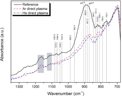
Normalized Fourier transform infrared spectroscopy spectra in attenuated total reflec-tion mode (FTIR-ATR) for InGaAs layers treated with plasmas and without pretreatment are depicted on figure 1. The bands observed in the 1100 – 1150 cm−1 and 1150 –
1200 cm−1 regions and accentuated by blue-grey rectangles are not attributed to InGaAs
oxides but might be related to carbonaceous pollution from Ge prism or samples. The principal absorption bands of the spectra are highlighted by vertical lines.
We clearly observe differences between the spectrum obtained for the reference sample and the spectra obtained for the plasma treated ones. Especially, the large absorption band in the region of 845 – 950 cm−1 and attributed to AsO
x(9, 10) is drastically reduced after
surface treatment. Bands located at 1066.4, 985.5, 904.5, 844.7 and 808.1 cm−1have been
assigned to As-O bonds (9–11) and the band located at 819.6 cm−1 is probably related
to As bond (12). On the whole, the bands assigned to As oxides (As-O or As-O-As bonds) appear to be less pronounced or even unobservable for the He plasma treated sample. Absorption bands located at 1083.8 and 1049.1 cm−1 have been related to InO
x
species (13). Looking at the shape and the intensity of these bands with accuracy might lead
Figure 1. Normalized FTIR-ATR spectra for InGaAs layers treated with Ar plasma (dash red line), He plasma (dash dot blue line) and without surface pretreatment (solid black line).
to the conclusion that Ar plasma seems to be more efficient for the removal of In oxides. The bands located at 788.8 and 763.7 cm−1 have been attributed to Ga-O bonds (9, 10).
Whatever the treatment involved, these two bands do not seem to be affected. Thus, the impact of plasmas on Ga oxides appears to be less pronounced. Because the band located at 869.8 cm−1does not seem to be impacted by the various plasma treatments, we assume
that it could be related to a Ga-O bond.
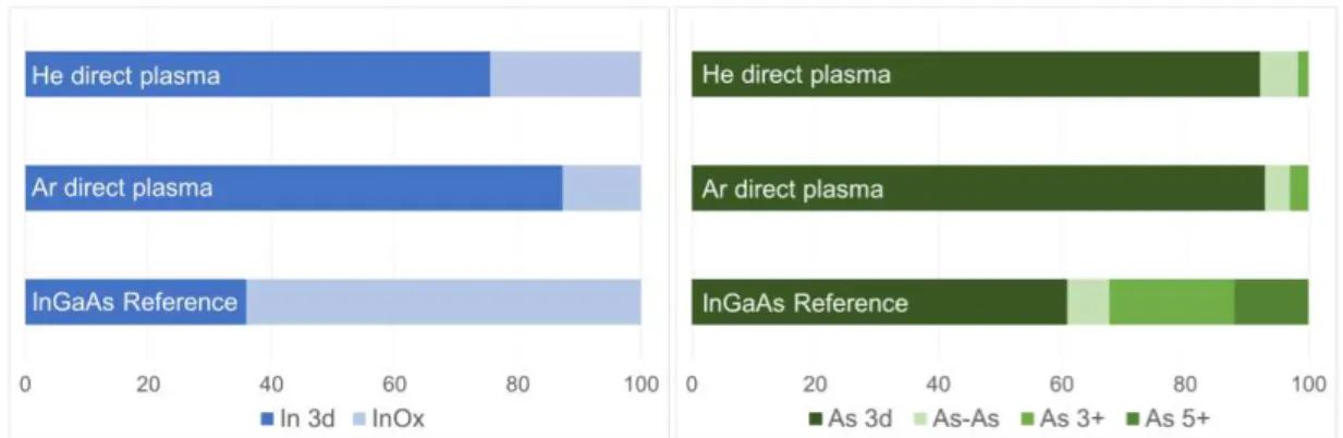
The FTIR-ATR characterisations have been supplemented by XPS analyses. From the fitted In 3d and As 3d XPS spectra (not shown here), we extracted on figure 2 the corre-sponding relative spectral weight of the different components. After plasma treatments, the fitting of Ga 2p XPS spectra were difficult to obtain with accuracy; moreover for Ga 3d region, the In 4d components tend to parasite the Ga ones. Thus, tendencies for Ga will not be discussed here. For In 3d region, spectra have been fitted using two components, the In 3d bulk peak and an InOx component located at approximatively + 0.8 eV from the bulk
peak. This latter corresponds to a mix of In+
and In3+
oxides. For As 3d region, spectra have been fitted using four components, the As 3d bulk peak, an As-As component located at + 0.75 eV from the bulk peak and related to arsenic dimers or dangling bonds at the surface (14), and As2O3 and As2O5 peaks respectively located at + 3.2 – 3.4 eV and + 4.4 – 4.6 eV from the bulk peak.
The XPS studies clearly evidence that both plasma treatments were efficient for reduc-ing the percentage of InGaAs oxides. It is obvious for As oxides where the As2O5 compo-nent is no more detected and the As2O3 is drastically reduced for treated samples. Even if the difference between the both plasmas is tiny, He direct plasma seems to be slighty more efficient for the removal of As oxides. Nevertheless, we believe that As oxide component is still detected because of the 30 to 45 minutes queue time between the sample treatments and the introduction of the samples under vacuum. Concerning, the removal of In oxides, we have evidenced that both plasmas significantly reduce the In oxide component. Indeed, for the reference sample, the In oxide component represents more than 60 percent whereas
Figure 2. Relative spectral weight of the components determined for InGaAs samples with various surface treatments for In 3d (left) and As 3d (right) regions.
for plasma treated samples the oxide component only corresponds to about 20 percent. XPS analyses tend to confirm the FTIR-ATR observations: Ar plasma is the most efficient for the removal of In oxides. Finally, for removing InGaAs native oxides, we have shown that both Ar and He plasmas were efficient .
Impact of plasma exposure of InP surfaces has also been studied. The figure 3 exhibits the relative spectral weight of the different components determined for argon and helium plasma treated samples and for an InP reference sample for In 3d and P 2p regions. For P 2p region, spectra have been fitted using two components, the P 2p bulk peak and an InPOx
component located at approximatively + 4.2 – 4.4 eV and related to In(PO3)3 or InPO4 species. The In 3d region is more delicate to fit ; four components have been used in order to obtain the most accurate fits. The In 3d bulk peak is completed by an InOx component
related to In2O3species and located at approximatively + 0.3 eV from the bulk peak and by an InPOxcomponent located at + 1.3 eV from the bulk peak and corresponding to In(PO3)3
or InPO4species. Finally, the fourth component, labelled In-, is located at approximatively - 1 eV from the bulk peak and is assigned to under coordinated indium at the surface or possibly indium dimers (14).
Figure 3. Relative spectral weight of the components determined for InP samples with various surface treatments for In 3d (left) and P 2p (right) regions.
Unlike the InGaAs layers, impact of direct plasmas on InP layers is less self-evident. Regarding the In 3d region, direct plasma treatments lead to the loss of the InPOx
com-ponent and to the increase of the In- comcom-ponent while the InOx component is practically
not impacted. The analysis of the P 2p region shows that the He plasma does not seem to
have any effect on the removal of the InPOx component whereas the Ar plasma treatment
appears to slightly reduce the oxide component. It is known that the oxidation of III-V semiconductors begins with the adsorption of oxygen on the Group V atoms (15) and that InP oxidation after air exposure is faster than the corresponding reaction of GaAs (16). Thus, the relative high percentages of InPOx component for the P 2p region and of InOx
component for the In 3d region are probably related to the air exposure of the samples be-tween the plasma treatments and the introduction under vacuum. Finally, these first results obtained for InP layers are mitigated. Either the plasma treatments involved are not effi-cient for the removal of InP oxides or the queue time observed between the treatment and the characterisation is prohibitive for characterising with accuracy the impact of treatments by XPS. This point will be further discussed in the next section.
Wet Chemical Cleaning Followed by In Situ Treatment
In order to study a full cleaning process, wet chemical treatments using HCl solutions were performed and followed by in situ plasma exposure. The figure 4 exhibits the nor-malized FTIR-ATR spectra obtained for InP samples with various surface treatments. The principal absorption bands of the spectra have been highlighted by vertical lines.
Figure 4. Normalized FTIR-ATR spectra for InP layers treated with degas treatment (dash orange line), HCl cleaning (dash dot dark cyan line), HCl cleaning followed by Ar plasma (short dash red line), HCl cleaning followed by He plasma (short dot blue line) and without surface pretreatment (solid black line).
The InP reference and the sample degassed at 200 °C for 30 s exhibit FTIR-ATR spec-tra different from the ones obtained for the samples treated by HCl solution and plasma exposure. Indeed, for these two samples, a large absorption band is seen between 950 and 1210 cm−1. This latter corresponds to the IR absorption of InP native oxides – mixture
of In2O3 and InPOx (17). As previously reported, many of the oxide vibrations involving
phosphorus (P-O stretch modes) are within the 900 – 1200 cm−1 range (18). After HCl or
plasma exposure, the large absorption band is no more observed. Instead, small and well-defined absorption bands are evidenced. This observation is correlated with the removal of
InP native oxides by the treatments involved and the regrowth of chemical oxides during the air exposure between the sample preparation and their characterisation. Based on lit-erature data, all the IR absorption bands have been identified. The bands located around 875 cm−1are assigned to the stretching mode of hydrogeno or dihydrogeno-phosphates that
can be present on the sample surface (19). The bands located at 1061.9 and 1082.2 cm−1
have been correlated with In2O3 or InO2 species (20). All the other bands are attributed to In(PO3)3and InPO4 species (21, 22). This observation is in good agreement with a previ-ous study which stated that for InP thermal and chemical oxides, InPOxare predominantly
present with a small mixture of In2O3species near the surface (17).
Thanks to these FTIR-ATR observations and the flagrant difference between the spectra obtained for treated and untreated samples, it appears reasonable to assume that the direct plasma treatments applied to InP layers and described in the previous section were, at least partially, efficient for the removal of InP native oxides and that the relative high proportion of oxide components measured by XPS is related to the regrowth of oxides during the queue time undergone by the samples between their treatment and their characterisation.
Based on the results obtained for the samples depicted on figure 4, it appears that a sin-gle degas step increases the oxide proportion compared to the reference sample. Moreover, even though a regrowth of chemical oxides is observed for all the treated samples, a simple wet cleaning appears to be less efficient than a wet cleaning followed by plasma exposure. Argon plasma seems to limit the regrowth of InPOx species (see the 1160 – 1180 cm−1
region) whereas the He plasma leads to a surface with less InOx species (see the 1060 –
1080 cm−1 region). These results have been correlated by XPS analyses (see the top part
of figure 5). XPS characterisations confirm that a single degas step leads to the increase of InOxand InPOxspecies proportions. Moreover, except for samples treated with a single
wet cleaning, all the tendencies observed by FTIR-ATR analyses have been confirmed dur-ing the XPS experiments. Indeed, the proportion of InOx species is slightly higher for Ar
treated samples while the He treated ones exhibit a higher proportion of InPOxspecies.
The bottom part of the figure 5 shows the relative spectral weight of the components determined for InGaAs samples exposed to various surface treatments. First, as observed for InP layers, a single degas step leads to the increase of InOxand AsOxspecies proportion
compared to the reference sample. The exposure of samples to a unique wet cleaning is efficient for removing In and As oxides but, especially for AsOx species removal, the
best results were obtained for a wet cleaning followed by plasma treatment. It should be noted that when combined to HCl solution cleaning, He plasma is the most efficient treatment for the removal of In and As oxides whereas when using plasma exposure alone, Ar treatment was more efficient than the He one for removing InOx species. Thus, using
a wet cleaning before plasma exposure must modify the surface and its reactivity towards plasma treatment.
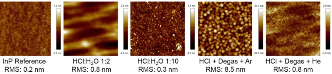
Finally, we have studied the impact of the various treatments involved in this study in terms of surface morphology and roughness. Whatever the surface treatment imposed to the InGaAs layers, no degradation of surface morphology and roughness was observed by AFM (images are not shown here). The RMS values obtained after surface treatments are similar to the one acquired for the reference sample (e.g. < 1.7 nm). On the contrary, InP surfaces appear to be greatly more sensitive to the surface treatments, results obtained for different samples are depicted on figure 6.
If concentrated HCl solutions (e.g. > 4 M) are efficient for the removal of InP oxides (see figures 4 and 5), they lead to a significant modification of the surface morphology
Figure 5. Relative spectral weight of the components determined for various treated sam-ples and for reference samsam-ples for InP In 3d (top left) and P 2p (top right) regions and for InGaAs In 3d (bottom left) and As 3d (bottom right) regions.
Figure 6. AFM images (scan size 1 × 1 µm) of InP samples for various surface treatments.
– RMS values slightly increase compare to the reference ones – and the appearance of boat-like shape of the etch pits is observed as already reported (4). Reducing the HCl con-centration (HCl:H2O 1:10) allows removing the InPOxand InOxspecies without damaging
the surface (RMS values are similar to the reference ones). The use of Ar direct plasma drastically impacts the surface morphology and its roughness. Indeed, the RMS values reach 8.5 nm, where the reference value is 0.2 nm, and dots appear at the surface of the samples. This impact on surface morphology is correlated with the increase on In-In bonds at the surface of InP layers (see the top left of the figure 5). This phenomenon could be related to a phosphorus depletion occurring at the indium phosphide surface (23, 24). On the other hand, wet cleaning followed by He plasma exposure appears to be less invasive for the surface. RMS values are similar to the ones observed for samples only treated with the wet cleaning. The difference between Ar and He plasma impact is attributed to the larger size and mass of the Ar ions.
Conclusions
In this work, we have investigated the impact of various plasma treatments on InGaAs and InP layers preceded (or not) by wet chemical cleanings based on HCl solutions. We have demonstrated that concentrated HCl solution cleanings followed by He direct plasma treat-ment are efficient for the removal of InGaAs native oxides without impacting the surface morphology and roughness. InP surfaces are greatly more sensitive to chemical and plasma treatments than the InGaAs ones. Nevertheless, we have highlighted that a He plasma ex-posure preceded by a diluted HCl solution cleaning appears to offer a good compromise between surface deterioration and native oxide removal.
Acknowledgments
The authors would like to thank Thierry Baron and his team (CNRS-LTM) for the realisa-tion of InGaAs and InP epitaxy.
This project was supported by the public grant ANR-13-NANO-0001 MOSINAS, the Equipex FDSOI11 projects and the French national program “Programme d’Investissements d’Avenir” IRT Nanoelec ANR-10-AIRT-05.
References
1. J. A. del Alamo, Nature, 479, 317 (2011).
2. X. Zhang, H. Guo, X. Gong, Q. Zhou, Y.-R. Lin, H.-Y. Lin, C.-H. Ko, C. H. Wann and Y.-C. Yeo, Electrochem. Solid-State Lett., 14, H60 (2011).
3. D. Liang and J. E. Bowers, Nat. Photonics, 4, 511 (2010).
4. D. Cuypers, S. De Gendt, S. Arnauts, K. Paulussen and D. H. van Dorp, ECS J. Solid State Sci. Technol., 2, P185 (2013).
5. S. Osakabe and S. Adachi, Jpn. J. Appl. Phys., 36, 7119 (1997).
6. D. H. van Dorp, S. Arnauts, D. Cuypers, J. Rip, F. Holsteyns, S. De Gendt and J. J. Kelly, ECS J. Solid State Sci. Technol., 3, P179 (2014).
7. D. Kikuchi, Y. Matsui and S. Adachi, J. Electrochem. Soc., 147, 1973 (2000).
8. Y. Sun, Z. Liu, F. Machuca, P. Pianetta and W. E. Spicer, J. Vac. Sci. Technol., A, 21, 219 (2003).
9. M. Rei Vilar, J. El Beghdadi, F. Debontridder, R. Artzi, R. Naaman, A. M. Ferraria and A. M. Botelho do Rego, Surf. Interface Anal., 37, 673 (2005).
10. N. Liu and T. F. Kuech, J. Electron. Mater., 34, 1010 (2005).
11. C. Bahr, A. vom Felde and M. Cardillo, J. Electron Spectrosc. Relat. Phenom., 54/55, 1075 (1990).
12. C. Lenczycki and V. Burrows, Thin Solid Films, 193/194, 610 (1990). 13. N. Liu and T. F. Kuech, J. Electron. Mater., 36, 179 (2007).
14. B. Brennan and G. Hughes, J. Appl. Phys., 108, 053516 (2010).
15. P. Pianetta, I. Lindau, C. M. Garner and W. E. Spicer, Phys. Rev. B, 18, 2792 (1978). 16. P. A. Bertrand, J. Vac. Sci. Technol., 18, 28 (1981).
17. N. Shibata and H. Ikoma, Jpn. J. Appl. Phys., 31, 3976 (1992).
18. O. Pluchery, Y. J. Chabal and R. L. Opila, J. Appl. Phys., 94, 2707 (2003). 19. O. Pluchery, J. E. Jr., R. L. Opila and Y. J. Chabal, Surf. Sci., 502/503, 75 (2002). 20. M. Yamaguchi, J. Appl. Phys., 53, 1834 (1982).
21. D. Ilieva, D. Kovacheva, C. Petkov and G. Bogachev, J. Raman Spectrosc., 32, 893 (2001).
22. J. E. Griffiths, G. P. Schwartz, W. A. Sunder and H. Schonhorn, J. Appl. Phys., 53, 1832 (1982).
23. J. E. Maslar, P. W. Bohn, D. G. Ballegeer, E. Andideh, I. Adesida, C. Caneau and R. Bhat, J. Appl. Phys., 73, 2983 (1993).
24. J. S. Pan, A. T. S. Wee, C. H. A. Huan, H. S. Tan and K. L. Tan, J. Appl. Phys., 80, 6655 (1996).