HAL Id: cea-01053354
https://hal-cea.archives-ouvertes.fr/cea-01053354
Submitted on 30 Jul 2014
HAL is a multi-disciplinary open access archive for the deposit and dissemination of sci-entific research documents, whether they are pub-lished or not. The documents may come from
L’archive ouverte pluridisciplinaire HAL, est destinée au dépôt et à la diffusion de documents scientifiques de niveau recherche, publiés ou non, émanant des établissements d’enseignement et de
Polishing-induced contamination of fused silica optics
and laser induced damage density at 351 nm
Jerome Neauport, L. Lamaignere, H. Bercegol, F. Pilon, J.-C. Birolleau
To cite this version:
Jerome Neauport, L. Lamaignere, H. Bercegol, F. Pilon, J.-C. Birolleau. Polishing-induced contamina-tion of fused silica optics and laser induced damage density at 351 nm. Optics Express, Optical Society of America - OSA Publishing, 2005, pp.10163-10171. �10.1364/OPEX.13.010163�. �cea-01053354�
Polishing-induced contamination of fused
silica optics and laser induced damage density at
351 nm
J. Neauport, L. Lamaignere, H. Bercegol
CEA Cesta, BP2, 33114 Le Barp, France
jerome.neauport@cea.fr
F. Pilon, J.-C. Birolleau
CEA Le Ripault, BP16, 37260 Monts, France
Abstract: In this paper we study the effect of contamination induced by
fabrication process on laser damage density of fused silica polished parts at 351 nm in nanosecond regime. We show, owing to recent developments of our raster scan metrology, that a good correlation exists between damage density and concentration of certain contaminants for the considered parts.
©2005 Optical Society of America
OCIS codes: (220.5450) Polishing; (140.3330) Laser damage; (160.2750) Glass and other
amorphous materials
References and links
1. M. L. André, "Status of the LMJ project," in Solid state lasers for application to Inertial Confinement Fusion:
Second Annual International Conference, M. L. André, ed., Proc. SPIE 3047, pp. 38-42 (1996).
2. W. H. Lowdermilk, "Status of the National Ignition Facility project", in Solid state lasers for application to
Inertial Confinement Fusion: Second Annual International Conference, M. L. André, ed., Proc. SPIE 3047, pp.
16-37 (1996).
3. H. Bercegol, P. Bouchut, L. Lamaignere, B. Le Garrec, G. Raze, "The impact of laser damage on the lifetime of optical components in fusion lasers," in Proceedings of Laser-induced Damage in Optical Materials : 2003, G. J. Exarhos, A. H. Guenther, N. Kaiser, K. L. Lewis, M. J. Soileau, C. J. Stolz, Eds, Proc. SPIE 5273, pp 312-324 (2004).
4. J. A. Menapace, B. Penetrante, D. Golini, A. F. Slomba, P. E. Miller, T. G. Parham, M. Nichols, J. Peterson., "Combined advanced finishing and UV-laser conditioning for producing UV damage resistant fused silica optics," in Proceedings Proceedings of Laser-induced Damage in Optical Materials, G. J. Exarhos, A. H. Guenther, N. Kaiser, K. L. Lewis, M. J. Soileau, C. J. Stolz, Eds, Proc. SPIE 4679, 56-68 (2001)
5. D. W. Camp et al., "Subsurface damage and polishing compound affect the 355 nm laser damage threshold of fused silica surfaces," in Proceedings of Laser-induced Damage in Optical Materials, Proc. SPIE 3244, 356-364 (1998).
6. M. D. Feit, A. M. Rubenchik, "Influence of subsurface cracks on laser induced surface damage," in Proceedings
of Laser-induced Damage in Optical Materials : 2003, G. J. Exarhos, A. H. Guenther, N. Kaiser, K. L. Lewis,
M. J. Soileau, C. J. Stolz, Eds, Proc. SPIE 5273, pp 264-272 (2004).
7. L. Gallais, P. Voarino and C. Amra, "Optical measurement of size and complex index of laser-damage precursors: the inverse problem," J. Opt. Soc. Am. B 21, 1073-1080 (2004).
8. B. Bertrussi, J. Y. Natoli, M. Commandré, "Effects of polishing process on silica surface laser-induced damage threshold at 355nm", Optics Com 242, Issues 1-3 (2004).
9. S. Papernov and A. W. Schmid, "Correlations between embedded single gold nanoparticles in SiO2 thin film and nanoscale crater formation induced by pulse-laser radiation," J. Appl. Phys. 92, 5720-5728 (2002). 10. F. Bonneau, P. Combis, J. L. Rullier, J. Vierne, H. Ward, M. Pellin, M. Savina, M. Broyer, E. Cottancin, J.
Tuaillon, M. Pellarin, L. Gallais, J. Y. Natoli, M. Perra, H. Bercegol, L. Lamaignere, M. Loiseau and J. T. Donohue "Study of UV laser interaction with gold nanoparticles embedded in silica," J. Appl. Phys. B 75, 803-815 (2002).
11. T. S. Izumitani, "Optical Glass," Kyoritsu Shuppan Company LTD Publishers (1985). 12. L. M. Cook, "Chemical proceeses in glass polishing," J. Non-Crys. Solid 120, 152-171 (1990)
13. H. Yokota, H. Sakata, M. Nishibori and K. Kinoshita, "Ellipsometric study of polished glass surfaces," Surface Science 16 (1969)
14. L. Nevot and P. Croce, "Caractérisations des surfaces par refléxion rasante de rayons X, application à l'étude du polissage de quelques verres silicates," Rev. Phys. Appl. 15 (1980)
15. J. P. Marioge, "Surfaces Optiques," EDP Sciences, pp 229-231 (2000)
16. M. R. Kozlowski, J. Carr, I. Hutcheon, R. Torres, L. Sheehan, D. Camp and M. Yan, "Depth profiling of polishing-induced contamination on fused silica surface," in Proceedings of Laser-induced Damage in Optical
Materials : 1997, G. J. Exarhos, A. H. Guenther, M. R. Kozlowki, M. J. Soileau Eds , Proc. SPIE 3244, 365-375
(1997)
17. L. Lamaignère, M. Loiseau, J.C. Poncetta and H. Bercegol, “Towards an Absolute Damage Density: The Rasterscan Procedure for Large Optics,” in preparation
18. M. Josse, R. Courchinoux, L. Lamaignere, J. C. Poncetta, T. Donval, H. Bercegol, "Computer-controlled measurements of laser-induced damage statistics on large optics," in Proceedings of Laser-induced Damage in
Optical Materials : 2004, G. J. Exarhos, A. H. Guenther, M. R. Kozlowki, M. J. Soileau Eds , Proc. SPIE 5647,
365-372 (2005)
1. Introduction
Lifetime in the UV of fused silica optics used in large high power laser facilities such as Megajoule laser (LMJ) [1] or National Ignition Facility (NIF) [2] has been the subject of extensive studies. It has been shown that at the wavelength of 351 nm the lifetime of fused silica optics is determined by both surface damage initiation and damage growth [3]. Hence, strategies developed to improve lifetime rely on reducing initiator density and using mitigation techniques to inhibit growth of damage sites induced by residual initiators [4]. As for the nature of damage initiators, it is now well admitted that they can be of two main kinds. A First possible source is subsurface cracks produced during grinding and polishing processes. This subsurface damage (SSD) is embedded under the polishing redeposition layer. Such discontinuities can locally enhance the electric field and be possible initiators [5]. It is possible to decrease laser induced damage density by applying grinding and polishing process variations that minimize SSD [6]. A Second possible source is nano-absorbing centers [7, 8]. If such absorbing centers haven’t been detected yet because of a lack of detectivity of existing characterization techniques, laser interaction experiments on gold nano particles embedded in silica have explored the validity of this hypothesis [9, 10].
We herein study the possible relationship existing between polishing induced contamination, as possible absorbing centers, and damage density at the wavelength of 351 nm. Chemo-mechanical description of the polishing process is widely admitted [11, 12]. During polishing, a modified layer, called polishing or Beilby layer is formed. Authors have measured the thickness of this layer to be in the range of approximately 10 to 100 nm [13, 14]. This modified layer is contaminated with polishing agents as seen by means of secondary ion mass spectroscopy (SIMS) [15]. Kozlowski et al. tried to correlate the level of polishing induced contaminants with the laser induced damage threshold of fused silica optics polished with different polishing agents (ceria or zirconia). They concluded that the correlation was weak at best [16].
The purpose of the present work is to give a new insight into the effect of polishing induced contaminants upon damage density of polished fused silica parts in the UV. In Section 2 of this paper, we give some information about sample manufacturing. Our raster scan damage testing procedure and its recent developments are described in Section 3. Surface layer analysis (Inductively Coupled Plasma Atomic Emission Spectrometer: ICP-AES) is presented in Section 4. Section 5 is devoted to the analysis and discussions of the obtained results.
2. Sample manufacturing
Seven 100mm diameter, 9mm thick fused silica samples were manufactured by two different vendors using various polishing processes. Samples were cut from Heraeus Suprasil 312 blanks. Parts were polished by two different vendors (A and B) with two different polishing processes. Vendor A used cerium oxide slurry. Vendor B used either cerium oxide or zirconium oxide slurry depending on the sample.
After polishing, some samples were exposed to post processing to modify the amount of polishing induced contaminants in the polishing layer and SSD. For this purpose, two types of post processing were used: acid etching with a 40% HF solution or reactive ion etching (RIE). Post processing was carried out on both sides of the sample with a constant material removal of 2µm per side. Sample preparation methods are summarized in Table 1.
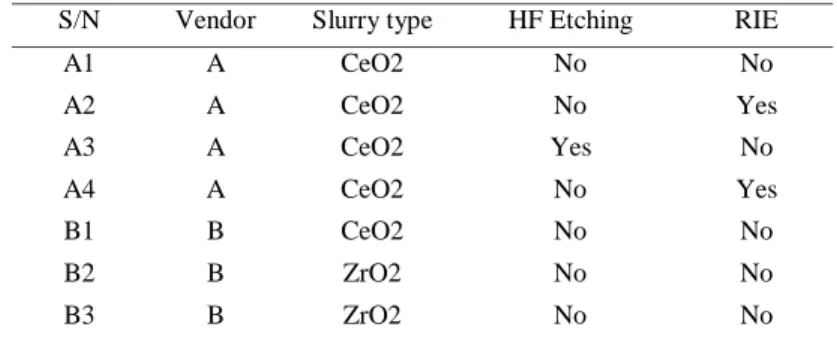
Table 1. Sample preparation methods
S/N Vendor Slurry type HF Etching RIE
A1 A CeO2 No No A2 A CeO2 No Yes A3 A CeO2 Yes No A4 A CeO2 No Yes B1 B CeO2 No No B2 B ZrO2 No No B3 B ZrO2 No No
Before damage testing, the samples were cleaned using a soap based cleaning procedure.
3. Damage density measurement : raster scan procedure
Raster scan damage test procedure is usually used to determine the optics damage density as a function of fluence. The goal of this test is to irradiate all the defects which could create damage. Tests are made with small beams. In order to scan the whole area, the optic to be tested is translated continuously along a first direction and stepped along a second direction. The beam overlap, shot to shot, is then a key parameter in order to well irradiate the sample. Repeating this test at several fluences on different areas permits to determine the number of damage sites versus fluence and then the damage density.
The source is a Nd:Yag laser manufactured by Coherent, frequency tripled with the following characteristics: wavelength-355 nm, single longitudinal mode and pulse duration-2.5 ns. During the test, the beam is focused on the sample surface in order to achieve high fluences; beam diameter is then about 400 µm at 1/e. The depth of focus is about 30 cm, much bigger than usual sample thickness (about 1 to 2 cm). Fluence fluctuations have a standard deviation of about 15% for this laser at 355 nm. When tens of thousands of shots are fired, we can get a total modulation of a factor of 2 in fluence. Thus, it is important to have access to the exact fluence of each shot in order to get a precise correlation between damage occurrence and laser fluence. During procedure, energy, spatial and temporal profiles, position of the beam on the sample are recorded for each shot in order to build up an exact fluence map, corresponding to the scan. A post-mortem observation of irradiated areas, by means of a long working distance microscope, gives an exact damage map. The minimum damage size detected is about 10 µm whatever the morphology of the damage.
Matching the two maps allows one to extract the shot fluence for each damage site. Data treatment is then realized by gathering damage in several fluence groups. With a fixed fluence, due to fluence fluctuations during the scan, damage density versus fluence is then determined on a large range.
Figure 1 illustrates typical results obtained after complete analysis. Blue points correspond to the treatment described previously. Due to Gaussian beam profile and beam overlap between shots (about 66%), we have to take into account the beam shape to obtain an absolute result. On the graph, one can observe two behaviors. Below 15 J/cm², damage density is roughly constant and damage is not fluence dependent but based only on the defect density; we simply have to take into account the total irradiated area. Above 15 J/cm², damage density increases following a power law. In this domain, damage occurs at the beam maximum fluence and only the Gaussian top part of the profile is taken into account. In this
case, raw data are corrected by a factor that depends on the slope of the fluence law [17, 18]. Ultimately, red points represent the absolute result from the test.
0,01 0,10 1,00 10,00 100,00 1000,00 10000,00 100000,00 0 5 10 15 20 25 30 Fluence (J/cm² @ 3ns) Dam a ge d en sit y (/ cm ²) treated data Power law Flat bottom Treated + corrected data
Fig. 1 : Damage density versus fluence. Sample B2. Blue and red points represent respectively treated and “treated + corrected” data. The corrective factors are 1.5 and 21 respectively for the flat bottom and the power law.
4. Redeposition layer contaminants characterization : ICP-AES analyses
The inductively coupled plasma atomic emission spectrometer (ICP-AES) used for the present work was an ACTIVA™ simultaneous solid state detector device (Jobin-Yvon – Horiba, Longjumeau, France). Operating conditions of the instrument are reported in the Table 2. The ICP-AES is equipped with a peristaltic pump for sample uptake. A blank solution is analyzed first, followed by sample solutions and multi-element calibration solutions.
Table 2. ICP-AES instrumental conditions
Spectrometer ACTIVA™ CCD detector 2048*512 pixels (13.5 µm*13.5 µm)
Frequency/MHz 40.68
Power/W 850 W-1500 W
Outer argon flow/l min-1 12 Intermediate argon flow/l min-1 0.15 Aerosol gas flow/l min-1 1
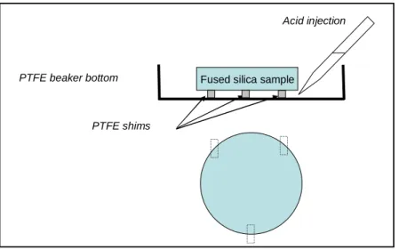
After accurate weighing and thickness measurement, each fused silica sample was etched (see Fig. 2) during 10 minutes in a mixture of ultra pure grade concentrated HNO3 and HF (90 %vol/10 %vol). Then the solution was sucked with a 3 mL tube as well as the de-ionized water used for washing. About 0.8 µm of silica was digested during this preparation.
Acid injection
PTFE beaker bottom Fused silica sample
PTFE shims
Fig. 2. Sample digestion scheme
This HNO3/HF cycle was repeated up to 8 times. This was generally enough to obtain
asymptotic impurities concentrations. After this controlled sample digestion, suitable spectra can be obtained for the main impurities (Ce, La, Zr, Hf, Al, Fe, Cu). The wavelengths used for ICP measurements are summarized in Table 3.
Table 3. wavelengths for impurities ICP measurements
Element Wavelength (nm) Ce 395.254, 413.380, 413.765 La 408.671 Zr 339.198, 343.823, 343.621 Hf 264.141, 282.022 Al 167.020, 396.152 Fe 259.940, 238.204 Cu 244.700, 324.754
5. Results and discussions
The seven manufactured samples were tested using the damage testing procedure detailed in Section 3. They mainly damaged on the exit face. The damaged side of each sample is then characterized owing to the method described in section 4. Elements introduced by the grinding or polishing processes and leading to strong absorption in the UV are monitored: Ce, Al, Cu, Fe, Zr, La. Each of them is tracked in the depth of the interface until signal goes to an asymptote consistent with bulk fused silica impurity content itself.
This analytical procedure allows us to evaluate concentrations of impurities as a function of depth. Figure 3 illustrates the surface and sub-surface depth profiles of impurities that can be obtained with this analytical procedure and gives by the way an average value for maximum depth of sub-surface cracks. Results are given with a relative precision of 10%.
Fig. 3. Depth profiles of impurities concentrations for sample B2
Because of its global surface digestion capabilities, such a procedure is of great interest compared to local (100x100µm2) SIMS analyses. However the analyzable surface can be reduced and localized to particular zones if necessary.
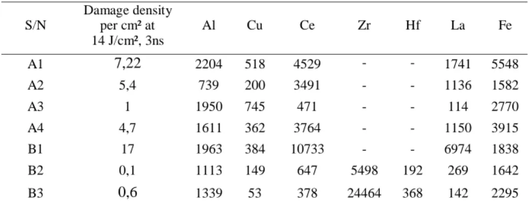
Table 4 gives the results of the damage and impurities measurement of the seven samples. In order to ease the analysis, we only study the damage density at a fixed fluence of 14 J/cm², 3ns pulse length. Regarding impurities, the cumulated amount of each contaminant in the interface is calculated expressed in nanograms. This quantity is then divided by the maximal depth where contamination is assumed to disappear, expressed in microns. For all the considered samples, this maximal depth is in the range of 5 to 10µm.
Table 4. Sample characterization: damage density and impurity concentration for each element in ng/µ m
S/N Damage density per cm² at 14 J/cm², 3ns Al Cu Ce Zr Hf La Fe A1 7,22 2204 518 4529 - - 1741 5548 A2 5,4 739 200 3491 - - 1136 1582 A3 1 1950 745 471 - - 114 2770 A4 4,7 1611 362 3764 - - 1150 3915 B1 17 1963 384 10733 - - 6974 1838 B2 0,1 1113 149 647 5498 192 269 1642 B3 0,6 1339 53 378 24464 368 142 2295
Note that cerium contamination is always associated with lanthanum since cerium slurries are most of the time a mix of both these elements. The same comment can be made with zirconium and hafnium. Dealing with zirconium polished parts B2 and B3, we can notice a small quantity of cerium existing in the polished part interface. The zirconium slurry used has been measured by ICP and is free of cerium. We believe that this cerium has been introduced by some polishing done with cerium slurry of another part on the polishing
0 200 400 600 0 1 2 3 4 5 6 7 8 9 Depth (µm) C onc ent rat ion ( µ g g-1) La Ce Al Fe Cu Zr Hf
machine before the manufacturing of our part. Insufficient cleaning of the polishing machine before the ZrO2 polishing of samples B2 and B3 is therefore likely to be the cause of the cerium pollution of these parts. Moreover, it must be noticed that a high concentration of zirconium is compatible with low damage density such as seen on part B3. This last remark has already been made [16]. Figure 4 shows the correlation existing between cerium content in the interface and damage density at 14 J/cm².
R2 = 0,9908 0 2 4 6 8 10 12 14 16 18 0 2000 4000 6000 8000 10000 12000 Ce (ng/µm) D a m a ge de ns it y / c m ²
Fig. 4. Effect of cerium content on damage density.
Data are fitted with a linear law with a correlation coefficient of 0.99 approximately. At the opposite, Figure 5 presents the data for Fe where correlation between damage density and Fe concentration is very weak.
R2 = 0,0012 0 2 4 6 8 10 12 14 16 18 0 1000 2000 3000 4000 5000 6000 Fe (ng/µm) D a ma ge de n si ty / c m ²
Table 5 details the correlation coefficients calculated for each element.
Table 5. Influence of each element on damage density
Element R² Ce 0,99 La 0,94 Al 0,16 Cu 0,03 Fe 0,001
Al, Cu and Fe contents have a very weak influence on damage density. On the contrary, cerium and lanthanum contents of the interface are closely related to the damage density at 14 J/cm². Since cerium absorption coefficient in the UV is strong [16], we believe this element is involved in the damage of our samples. We can also notice that for low cerium concentration samples (A3, B2 and B3) this correlation is weaker since damage density is varying up to a decade while cerium vary of a factor of 2. It could mean that the role of cerium is less prevalent for samples with damage density of less than one damage per cm². More extensive studies of low damage density samples would be needed to give a clear insight of this phenomenon.
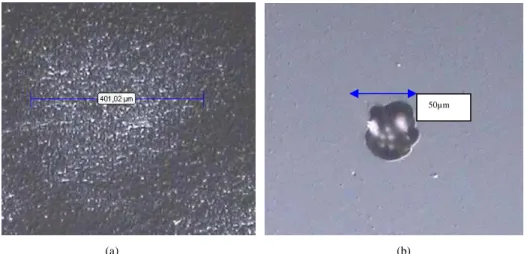
We have also been trying to correlate the presence of cerium in the interface with damage morphology. On part B1 exhibiting very high cerium concentration in the interface, the "gray haze" damage morphology can be easily seen such as previously described by Kozlowski et al. [16]. Figure 6(a) shows such a gray haze damage like observed with a Nomarski microscope. When cerium content decreases, the gray haze morphology disappears to leave place to more classical small damage sites such as depicted in Figure 6(b). Some small damage clusters can be observed but no clear correlation has been seen between cerium concentration and quantities of these clusters like damage sites.
(a) (b)
Fig. 6. (a) Gray haze damage, part B1 (b) typical damage morphology on part A4
6. Conclusion
We have demonstrated that for polished fused silica parts having a damage density in the range of 1 to 100 damage per centimeter square at 14 J/cm², 3ns, cerium contamination induced by the polishing process is likely to be involved in the damage mechanism. This has been shown using two types of polishing processes in combination with various post
processing steps. In terms of damage morphology, no specific morphology could be associated with this cerium pollution at low damage density.
Acknoledgments
We would like to gratefully acknowledge the help of P. Bouchut and colleagues from CEA Leti for conducting HF etching and cleaning of our samples.