Commercialization Potential of Dye-Sensitized Mesoscopic Solar Cells
by Kwan Wee Tan
B.Eng (Materials Engineering) Nanyang Technological University, 2006
SUBMITTED TO THE DEPARTMENT OF MATERIALS SCIENCE AND ENGINEERING IN PARTIAL FULFILLMENT OF THE REQUIREMENTS
FOR THE DEGREE OF
MASTER OF ENGINEERING IN MATERIALS SCIENCE AND ENGINEERING AT THE
MASSACHUSETTS INSTITUTE OF TECHNOLOGY SEPTEMBER 2008
© 2008 Kwan Wee Tan. All rights reserved.
The author hereby grants to MIT permission to reproduce and to distribute publicly paper and electronic copies of this thesis document in whole or in part in any medium now
known or hereafter created.
Signature of Author ……….... Department of Materials Science and Engineering July 16, 2008 Certified by ...………...
Yet-Ming Chiang Kyocera Professor of Ceramics Thesis Supervisor Certified by ...………...
Chee Cheong Wong Associate Professor, Nanyang Technological University Thesis Supervisor Accepted by ………....
Samuel M. Allen POSCO Professor of Physical Metallurgy
Commercialization Potential of Dye-Sensitized Mesoscopic Solar Cells By
Kwan Wee Tan
Submitted to the Department of Materials Science and Engineering on July 16, 2008 in partial fulfillment of the requirements for the Degree of Master of Engineering in Materials Science and Engineering
ABSTRACT
The price of oil has continued to rise, from a high of US$100 per barrel at the beginning 2008 to a new record of above US$140 in the recent weeks (of July). Coupled with increasing insidious greenhouse gas emissions, the need to harness abundant and renewable energy sources is never more urgent than now. The sun is the champion of all energy sources and photovoltaic cell production is currently the world’s fastest growing energy market.
Dye-sensitized solar cells (DSCs) are photoelectrochemical cells which mimic the natural photosynthesis process to generate solar electricity. Typically, a monolayer of dye sensitizer molecules is anchored onto a semiconductor mesoporous film such as TiO2 to
generate charges on exposure to illumination. The nanocrystalline particulate three-dimensional network provides high surface area coverage for the photogeneration process and percolation of charges.
In the thesis, we will review the current research efforts to optimize the DSC performance and develop probable applications to complement existing solid-state photovoltaic technologies. We believe the large and rapidly expanding solar market offers a prime commercial opportunity to deliver a DSC product for mass adoption by consumers. DSC is kept at a low production cost because it bypasses conventional vacuum-based semiconductor processing technologies, instead relying on solution and chemical processing routes. However, our cost modeling analysis show the TCO glass substrate and ruthenium dyes could constitute more than 90% of the overall materials cost. Thus, we recommend new technological approaches must be taken to keep the substrate pricing low and continuously improve the energy conversion efficiencies to further lower the production cost.
Thesis Supervisor: Yet-Ming Chiang Title: Kyocera Professor of Ceramics Thesis Supervisor: Chee Cheong Wong
ACKNOWLEDGEMENTS
First and foremost, I would like to express my sincere appreciation to my thesis advisor, Professor Yet-Ming Chiang, for offering me an once-in-a-lifetime opportunity to learn under his kind guidance and philanthropic sharing of his entrepreneurship experience. Also, I want to show appreciation to my thesis co-advisor, Professor Chee Cheong Wong, for amicably welcoming me back into the NTU research team with open arms. He will always provide new invigorating ideas and suggestions to make my life a little more interesting and challenging everyday.
Special mentions to go out to my fellow SMA dear friends and student colleagues for their company through thick and thin in our short but definitively memorable moments that I will look back fondly. Despite being the OLDEST, I have definitely learnt a lot more from everyone, the young and younger. Whether you are the Singaporean Prof Wii, BFG or the Harvard–MIT Hall King; a PRC Chinese non-gay, henpecked (two in fact) and formidable MIC LG brand; an Indonesian forever-kid and another probable-reformist; a Malaysian mama; or Indian monkeys (three in all, one totally not reliable!), the question-problem-kid, and Indian prince, keep in touch!
I guess it is better to list out each and everyone in case memory loss hits me later. They are, and not in the order of merit: Li Guang, Fidelia, Ha, Man Yin, Yuyan, Zhoujia, Song Yang, Luo Jia, Henry, Qixun, Beng Sheng, Weimin, Wardhana, Manik, Kunal, Raju, Raghavan, Anay, Liu Chao, Du Lei, An Tao and Handra.
Specifically, I have gained tremendous help and knowledge from the constructive discussions with Dr Yan Qingfeng, Mr Yip Chan Hoe and Mr Kunal Mukherjee. Thanks and I have learnt a lot more than I possibly could within such a short span of time.
Most importantly, my deepest heartfelt gratitude to my parents for all the love, joy happiness and sacrifices in ensuring that I receive the best in life, and my siblings for their unreserved support and patience.
Lastly, I thank the Massachusetts Institute of Technology for giving me a first-rate education and the Singapore-MIT Alliance for financial support.
Table of Contents
1. Introduction... 6
1.1 Background ... 6
1.2 Thesis Outline ... 9
2. Solar Photovoltaic Technologies... 10
2.1 Some Important Definitions[17]... 10
2.2 Silicon Solar Cells[18]... 13
2.3 Cadmium Telluride[25] (CdTe) ... 17
2.4 Copper Indium Gallium Di-Selenide[27] (CIGS)... 17
2.5 III-V Compound Semiconductors[18]... 19
2.6 Overview... 22
3. Nanostructured Photoelectrochemical Solar Cell ... 24
3.1 Grätzel Cell ... 24
3.2 Energetics and Dynamics of Operation[34,36]... 25
3.3 DSC Materials Selection... 29
3.3.1 Equivalent Circuit for DSCs ... 30
3.3.2 Wide Energy Bandgap Semiconductor Materials for Electrode... 32
3.3.3 Photosensitizers... 33
3.3.4 Electrolytes ... 36
3.4 Nanoarchitectures for DSCs ... 38
3.4.1 Nanowire and Nanotube DSCs ... 38
3.4.2 Photonic Crystal DSC ... 41
3.5 Discussion ... 44
4. Market Analysis and Opportunities... 46
4.1 Overview... 46
4.2 Opportunities... 47
4.2.1 Talk about market drivers/silicon and thin film... 47
4.2.2 United States and the European Union ... 48
4.2.3 Asia and Singapore ... 49
4.3 Technology Trend... 50
5. A Technopreneurship Case Study... 51
5.1 Product Offering ... 51
5.2 Competition and Competitive Advantages ... 53
5.2.1 Competing Solar Photovoltaic Technologies... 53
5.2.2 Competitive Advantages... 54
5.2.3 DSC Company Profilies[22]... 55
5.3 Supply Chain... 56
5.4 Intellectual Proprietary... 57
5.5 Cost Model... 61
6. Conclusion ... 65
7. References... 67
1. Introduction
1.1 Background
Oil prices ended the year 2007 near US$96 a barrel.[1] Fast forward to June 2008, the prices have risen by 50% close to US$150 due to the weakening US dollar, rising demand in the booming India and China economies, as well as geopolitical instabilities in Nigeria and Middle East.[2] Protests against surging fuel prices have triggered fears of political instability and a global economic downturn in Asia and Europe.[3] And if the situation is not any worse, the recent report of the United Nations Intergovernmental Panel on Climate Change (IPCC) has asserted that changes in the atmosphere, the oceans and glaciers and ice caps have proven unequivocally that the world is warming due to the increase in greenhouse gas concentrations.[4] A temperature rise of 0.6 ± 0.2 °C has already taken place in the 20th century and an increase of 1.8-4.0 °C is estimated in the next century. Without any doubts, energy is now the most important technological problem in the world.[5]
Energy is a commodity, the currency that is providing the livelihood for people and driving the global economy. At present, humans consume approximately 15 TW in a typical year.[5] Eighty-five percent of that amount is represented by fossil energy, with oil,
natural gas, and coal contributing with amounts of 36.4%, 23.5% and 27.8%, respectively.[6] The rest of the power is generated by hydroelectricity, biomass, nuclear
fission and renewable resources.[5] Solar electric power production generated by solar
photovoltaic (PV) devices is growing rapidly: providing 10 parts of a million in 2001, and now supplying 0.03% of the total global primary power with a historical average growth of 37% in 2007.[5,7] The sun is the champion of all energy renewable or non-renewable sources and provides the Earth with 120,000 TW.[8] To put in a simpler way, more energy from the sun hits the earth in one hour than all of the energy consumed on our planet in the entire year. Ironically the most expensive electricity comes from solar photovoltaic power production. Based on US energy consumption in 2002, solar electricity costs around 25-50 cents per kWh to produce and coal is the cheapest, costing 1-4 cents per kWh and supplying almost 50% of the electricity in US and up to 80% in China.[5] As
such, renewable solar photovoltaic power must decrease by a factor of 25-30 to compete economically in the global energy production arena. Figure 1.1 compares the costs and performance of solar energy to those of biofuels and wind from the same land mass.[5]
Despite the associated high costs, demand of electrical power from the space industry in the 1960s and the oil price hikes in 1970s and 2000s were sufficient to push for adoption of PV technology research and markets.[9] Annual production first exceeded 1 MWP in
the 1970s, 2000 MWP in 1999, and jumped to 3800 MWP in 2007.[10] Expansion of
conventional solid state solar cell production and rapid growth of non‐silicon technologies is estimated to rapidly increase cell/module production to more than 20 GW in 2011.[11] Growing by an impressive average of 48 percent each year since 2002, PV production has been doubling every two years, making it the world’s fastest‐growing energy source.[10]
Wafer‐silicon solar cell technologies are currently the dominant commercial PV technology by a huge margin (90% in 2000)[12] and are likely to remain so for at least 10 years.[13] A major competitor is the non‐silicon thin film PV technologies which cost less and their physical flexibility makes them more versatile than traditional solar cells. One example is the dye-sensitized solar cell (DSC) technology which has superior performance compared to silicon solar cells under diffuse light conditions. The global market demand for thin film PVs grew from 4% in 2003 to 7% in 2006.[10] By 2010, the production of non‐Si based PV systems is estimated to reach 2 GW[11] and grabbing 20% of the market share[10].
Nanomaterial science and technology has brought about fast growth of new generation solar cells which consist of nanostructures using nanoscale materials and fabricated by nanotechnologies.[14] Third generation photovoltaics such as the DSC do not depend on conventional critical parameters such as minority carriers or internal electric field to generate solar electricity. Instead, the dye cell mimics photosynthesis and physically separates the photon absorption and charge percolation processes. Certified efficiencies
tandem versions have reached 15% conversion efficiencies[16]. DSCs have special potential for electricity generating/conserving windows and other building-integrated photovoltaic (BIPV) components, and for lightweight portable power-supplying charging devices for consumer electronics and military applications.[13]
(a)
(b) (c)
Figure 1.1 (a) Progress of research-scale photovoltaic device efficiencies under AM1.5
stimulated solar illumination, (b) Gross energy output (million kWh per hectare) and cost (cents per kWh) of resource produced from 1 hectare of land for several renewable sources of energy, and (c) cost-efficiency analysis for I, II, and III generation of PV technologies.[5]
1.2 Thesis Outline
In Chapter 2 and 3, we briefly review the various solar photovoltaic technologies and the ongoing research and developments of DSCs. Chapter 4 provides an overall picture of the global and regional market for photovoltaic devices. Finally in Chapter 5, we would execute a technical case study to look into the commercialization potential of the DSC technology and applications. Specifically, we will detail the technology risks, how it fits in with competing technologies, potential applications, and how these needs are served today and near future.
2. Solar Photovoltaic Technologies
The solar cell is the basic building block of photovoltaics that converts sunlight into electricity. Conventional solid state PV devices are built on charge separation at the interface of a p-n junction of silicon and other semiconductors. Novel nanostructured materials synthesized in recent years are now challenging the dominance of inorganic solid state junction devices with a new generation of nanoscale solar cells having very different operating mechanisms. We would briefly explore the key fundamental concepts and various genres of solid-state PV technology.
2.1 Some Important Definitions
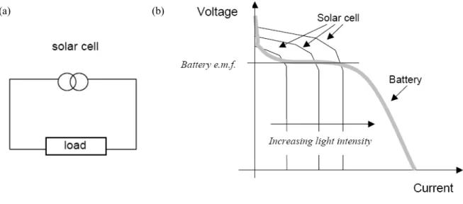
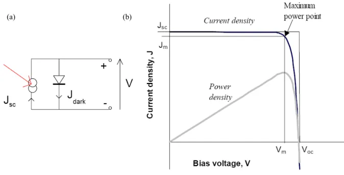
[17]In Fig. 2.1, a conventional solid-state solar cell replaces the battery and acts as constant current source in a simple circuit. Under illumination, the cell develops a voltage and switches on. For any intermediate load resistance RL, the cell develops a voltage between
0 and VOC (open circuit voltage) to drive a current I such that V = IRL. I(V) is determined
by the current-voltage characteristics of the cell under the light. A more common unit is the short circuit current density JSC.
(a) (b)
Figure 2.1 (a) Schematic diagram of a solar cell replacing a battery in a simple circuit, and (b)
voltage-current curves of a conventional battery (grey) and a solar cell under different levels of illumination.[17] A photovoltaic cell is essentially a current source that delivers a constant current
for any given illumination level while the voltage is determined largely by the resistance of the load.
Quantum efficiency QE is a key quantity which describes solar cell performance under different conditions and relates to the photocurrent density JSC under irradiance. It is
defined as the probability that an incident photon of energy E will deliver one electron to the external circuit. Thus,
( )JSC =q b E QE E dE
∫
S ( ) (2.1)where bS (E) is the incident spectral photon flux density, the number of photons of energy
in the range E to E + dE which are incident on unit area in unit time, and q is the electronic charge. QE depends upon the absorption coefficient of the solar cell material, the efficiency of charge separation and the efficiency of charge collection but not on the incident spectrum.
When a load is present, a potential difference develops to generate a rectifying current that acts in the opposite direction to the photocurrent. This reverse current is usually called the dark current Idark (V) that flows across the device under an applied bias V in the
dark. For an ideal diode the dark current density Jdark (V) is expressed as,
0 ( ) B 1 qV k T dark J V =J e⎛⎜⎜ − ⎞⎟⎟ ⎝ ⎠ (2.2)
The sign convention in PVs is such that the photocurrent is positive. Thus, the net current density in the cell is,
( )J V =JSC −Jdark( )V (2.3)
When the contacts are isolated, the potential difference has its maximum value, the open circuit voltage VOC, which is equivalent to the condition when the dark current and short
circuit photocurrent exactly cancel out.
ln 1 B SC OC dark k T J V q J ⎛ ⎞ = ⎜ + ⎟ ⎝ ⎠ (2.4)
The cell power density reaches a maximum at the cell’s operating point which occurs at some voltage Vm with a corresponding current density Jm as shown in Fig. 2.2. The fill
m m SC OC J V FF J V = (2.5)
and describes the squareness of the J-V curve. The efficiency η is the power density delivered at operating point as a fraction of the incident light power density, PS,
SC OC S
J V FF P
η= (2.6)
Another common mode of representing conversion efficiency in literature is the Incident Monochromatic Photon-to-Current Efficiency (IPCE) or External Quantum Efficiency (EQE) which is calculated in the following,
2
2
1250 photo current density [ A/cm ]
wavelength [nm] total incident photon flux [W/m ]
IPCE= × μ × (2.7) or, inj C IPCE=LHE×φ ×η (2.8) and ( ) ( ) 1 10 LHE λ = − −Γσ λ (2.9)
where LHE is the light harvesting efficiency, Γ is the number of moles of the sensitizer per cm2, σ is the absorption cross section of the sensitizer molecule, inj is the electron
injection efficiency and ηC is the electron collecting efficiency at the back contact. IPCE
includes the effect of optical losses such as transmission and reflection. Internal quantum efficiency (IQE) refers to the efficiency in which photons that are not reflected or transmitted out of the cell can generate collectable carriers. IQE is expressed as,
IPCE IQE
LHE
= (2.10)
For classification purposes, the solar cell device is usually illuminated with a stimulated air mass (AM) spectrum, AM0 for space applications and AM1.5 for terrestrial applications. The AM1.5 spectrum is the global average incident at the surface of the Earth when the path length through the Earth’s atmosphere/height of the atmosphere, sec θ = 1.5. The power of radiation incident P is 1367 W m-2 and 963 W m-2 for the AM0 and AM1.5 spectrums, respectively.
(a) (b)
Figure 2.2 (a) Equivalent circuit of an ideal solar cell, and (b) current voltage (black) and
power-voltage (grey) characteristics of an ideal cell.[17] If the fill factor FF = 1, the current voltage curve
would follow the outer rectangle.
2.2 Silicon Solar Cells
[18]Silicon (Si) has an indirect bandgap ~ 1.1 eV that explains for the low optical absorption coefficient (α ~ 100 cm-1). For a 90% light absorption, it requires only 1 μm of GaAs (a direct semiconductor) compared to 100 μm of crystalline silicon.[19] As such, typical unsophisticated cells must be at least 250 µm thick to absorb all the active wavelengths in sunlight with reasonable efficiency.[9] The best laboratory AM1.5 efficiency for single crystal silicon is currently at 24.7%,[19,20] whilst the commercial wafer-based Si solar cells has a maximum efficiency of 16-18% only in bright sunlight,[12,20,21] meaning it is highly sensitive to the incidence and intensity of light. Also, the Si wafers are fragile and the high-temperature processing steps severely limit ramping up the production capacity.[12] Other critical issues[22] using Si for solar energy generation include: (1) high cost of raw materials, (2) significant energy requirements for manufacturing that hinder significantly commercial viability, (3) negative environmental by-products of the manufacturing process, and (4) sub-optimal economics without public financial investments.
In a classical Si solar cell structure below in Fig. 2.3(a),[18] the boron doped p-type monocrystaline Si wafer is sawn from a boule of silicon grown using the Czochralski method and the p-n junction formed by diffusing phosphorus impurities into the wafer. Screen printed silver contact fingers are used on the n-type surface to make both electrical contact and to allow light to be transmitted to the junction region. Aluminum paste is used to make contact at the back p-type surface. The PV device is annealed to introduce a p+ doped region at the back of the cell to lower the contact resistance and supply a back surface field that reflects minority carriers back towards the junctions. Furthermore, the cell surface is textured to minimize reflection and to refract light to high angles of refraction to enhance the path length of the light within the Si. An antireflection coating (such as TiO2) is deposited over the top contact fingers to complete the device.
(a) (b)
Figure 2.3 (a) Schematic cross-sectional view of a silicon solar cell with screen printed
contacts.[18] (b) Illustration of a Sanyo high-efficiency Si heterojunction with intrinsic thin layer
(HIT) solar cell that has an efficiency of up to 22.3%.[5]
Bulk-Si-based PV devices are usually manufactured using Czochralski, multicrystalline, float-zone wafers, and melt-grown crystals such as silicon ribbons that are about 100 μm or thicker.[18] The Si ribbon solar cells have conversion efficiencies over 15%. There are two main fabrication approaches. In the edge-defined film-fed growth process (ASE Americas), a self supporting 2D sheet of Si is pulled from the melt through a die to give the shape of the ribbon consisting of octagon tubes of 5.3 m length and a nominal average wall thickness of 280 μm cut by laser ablation.[18,19] Alternatively, utilizing the string ribbon process developed by Evergreen Solar, Si ribbons of variable thickness are pulled
into the desired length with diamond tools.[19] The speed is up to 25 mm per minute, resulting in ribbons with a thickness below 100 μm.[19]
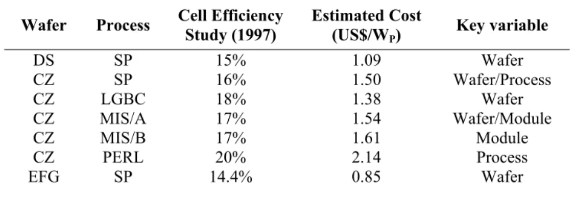
A study was conducted under the European Union Photovoltaic Program (1997) involving seven major European photovoltaic manufacturers and research laboratories to compare a number of important Si solar cell technologies: EFG ribbon, multicrystalline and crystalline wafer technologies, and between screen-printed, buried-contact, metal– insulator–semiconductor and PERL (passivated emitter, rear locally diffused cell) processing approaches as tabulated in Table 2.1 below.[9] From the collected data, EFG ribbon produces the lowest cost compared to screen-printed cells. The advantage of the ribbon stems from the fact that it does not need to be sawn. In terms of the different processing approaches, the cheapest is the buried-contact due to the increased efficiency giving more power per unit process area over the screen-printing process. However, despite the initial optimism that EFG ribbon technology would dominate production, the market share has remained small at 1% of the total sales.[18] The key assumptions made in this study are manufacturing volume is set to 500 MWP of solar cells per annum and the
material cost of silicon source is US$25 per kg.
Table 2.1 Summary of published results of a European Commission study of manufacturing costs
for 500 MWP per year factory.[9]
Wafer Process Cell Efficiency
Study (1997)
Estimated Cost
(US$/WP) Key variable
DS SP 15% 1.09 Wafer CZ SP 16% 1.50 Wafer/Process CZ LGBC 18% 1.38 Wafer CZ MIS/A 17% 1.54 Wafer/Module CZ MIS/B 17% 1.61 Module CZ PERL 20% 2.14 Process EFG SP 14.4% 0.85 Wafer
DS: directional solidification; CZ: Czochralski growth; EFG: edge-defined film-fed growth; SP: screen-printed; LGBC: laser grooved, buried-contact; MIS/A: metal–insulator–semiconductor; MIS/B: as for MIS/A but with resin-fill packaging; PERL: passivated emitter, rear locally diffused.
Reducing the thickness and purity of silicon is desirable to reduce materials usage and lower processing costs for economical reasons. These parameters also improve the manufacturing flexibility to higher levels of production automation. Amorphous-silicon (a-Si) thin-film modules that constitute a majority of thin film Si PV production, was about 100 MW worldwide in 2006.[23] A doubling of the annual a-Si production rate to 200 MW is likely expected by 2008.[23] The module efficiencies are in the range of 6-8% at prices competitive with wafer Si.[19,23] Typically less than 2 μm, a-Si cells are produced by chemical vapor deposition (CVD) of gases containing silane (SiH4) at temperatures
below 300 °C.[18] The material consist of an alloy of Si and hydrogen (5% - 20% atomic hydrogen) with a direct bandgap of 1.7 eV and an optical absorption coefficient of α > 105 cm-1. The disorder in Si:H based materials transforms the nature of optical absorption associated with the indirect bandgap Si to that of a direct bandgap compound semiconductor, and thus only a few microns of material are needed to absorb most of the incident light, reducing materials usage and hence cost. Initially attaining a high efficiency of 12% in the laboratories, a-Si commercial cells suffer light-induced degradation when exposed to sunlight over a certain period known as the Staebler-Wronski effect on the carrier-transport in the thin film Si cells. Hence a-Si cells are rated in the stabilized condition only which occurs after about 100 hours exposure to light. Mainly for indoor use, a-Si modules current account for less than 6% of the number sold for use in commercial systems.[5,18,23]
Norway’s Renewable Energy Corporation (REC) has recently announced to build a new integrated solar manufacturing facility in Singapore.[24] This manufacturing complex will incorporate wafer, cell and module production facilities with a production capacity of up to 1.5 GW. The company is organized into three divisions: REC Silicon and REC Wafer that produces polysilicon and wafers, and REC Solar to fabricate solar cells and solar modules.
2.3 Cadmium Telluride
[25](CdTe)
CdTe is a direct semiconductor with an energy bandgap of 1.45 eV, and is therefore very well adapted for efficient conversion of solar light into electricity.[9] Fig. 2.4 shows the cross-sectional SEM image of a CdTe thin film layer with an ideal 5 μm thickness.[5] At present, commercial CdTe solar cell modules achieve a high AM1.5 efficiency of 16.5%.[20,25] However, the VOC in CdTe solar cells is only 880 mV which is 20% below
that of III-V solar cells with similar bandgaps.[9] This V
OC deficit has many contributing
causes, namely (1) a lack of clear understanding of working principle of CdTe solar cell device operation, (2) the inability to model and predict device performance, (3) the lack of control of carrier concentrations in the absorber layer and (4) no well-defined and robust back contacts. Enhanced VOC with some improvements from JSC in the thin-film
CdTe devices will most likely be the pathway to higher cell and module efficiency. Due to the toxic nature of Cd, environmental, safety, and health continues to be an important aspect of the technology development. The CdTe system installation cost is calculated to be US$4-5 per watt and set to be lowered to US$2 per watt by 2015 by the US Department of Energy.[25] Recently, First Solar has reported their CdTe thin film solar cells have a substantially lower manufacturing cost at US$1.25/WP with an efficiency of
9% and thickness of less than 3 µm on glass platforms.[5] Under the US Solar America Initiative (SAI) – Technology Development program, AVA Solar and Primestar Solar have been awarded US$3 million to develop commercial CdTe thin film modules to achieve annual production capacities of 3 MW by 2008 and up to 200 MW by the former in 2010.[26]
2.4 Copper Indium Gallium Di-Selenide
[27](CIGS)
Ternary compound semiconductors such as CIGS is a very promising semiconductor material with a high optical absorptivity that allows 99% of available light to be absorbed in the first micron of the material.[28] Thus far, the cell has achieved a high AM1.5 efficiency of 19.9% in laboratory specimens and 13.4% for a (Showa Shell) module size.[20] With efficiencies of only 8%–10%, good production yields (>70%), and
sell their modules profitably for less than $2/Wp. Unfortunately, manufacturing
efficiencies have hit a bottleneck of 11% efficiency with an annual power degradation of 6% in the pilot CIGS solar cell arrays. But more importantly, the ultimate impact of CIGS PV technology may be limited by the availability of indium. Estimates vary widely, but based on what is known today about indium usage and supply, a range of 2,000–10,000 MWP of annual module production may perhaps be established as a limit. To extend these
limits, it would be highly desirable to use CIGS devices with much thinner absorber layers than used today around 1.4 µm.[5] This would also increase manufacturing throughput because thinner layers can be deposited in less time. Implementation will require the development of thin absorber cells without a loss in efficiency, processing robustness, and module reliability.
Shell Solar and Global Solar have played major roles in the development of first-generation CIGS technology to bring to commercialization. Global Solar is the only company to date to fabricate CIGS on a flexible substrate and distribute foldable and glass products manufactured utilizing a "roll-roll" process that is significantly more cost-effective than traditional in-line manufacturing approaches.[28] Similar to AVA and Primestar, SoloPower has received US$2.37 million to develop an electroplating-based CIGS cell and module manufacturing technology with an annual production of 120 MW by 2010 under the SAI Photovolatic Technology Incubator Program.[26]
(a) (b)
Figure 2.4 (a) Cross-sectional SEM micrographs of a CIGS solar cell (left) and a CdTe cell
2.5 III-V Compound Semiconductors
[18]III-V Materials such as gallium arsenide (GaAs), indium phosphide (InP) and gallium antimonide (GaSb) have direct energy bandgaps, high optical absorption coefficients and good values of minority carrier lifetimes and mobilities (in highly pure, single crystal material) making them excellent materials for making high efficiency solar cells. A detailed analysis shows that for the AM1.5 spectrum the optimum energy band gap is 1.5 eV, that is, close to the energy band gaps of the compound semiconductors such as InP (1.34 eV) and GaAs (1.424 eV).[18] Thus, very thin cells can be produced to take advantage of their high absorption coefficients.
GaAs and InP are most commonly used in single junction (SJ) solar cells. One of the first GaAs based solar cells was a p-n junction device with an AM1 efficiency of 11%,[18] and a p-AlGaAs/n-GaAS heterojunction cell which achieved an AM1 efficiency of 15.3%[9]. However, the major disadvantage using III-V compounds in PV devices is the very high cost of producing device quality epitaxial layers of the compound semiconductors. Moreover, the materials can be easily cleaved and are significantly mechanically weaker than Si despite their high density. However, the potential for high conversion efficiencies combined with radiation resistance in the demanding environment of space power generation alleviate against the high materials cost. Firstly, high performance III-V cells can be made significantly thinner than Si based devices. Most of the photons and electrons pass through the thin active region and cause minimum lattice damage. In addition, InP based devices provide even higher performance and resistance to radiation damage than even GaAs and Si cells due to the electronic annealing enhancement of major defect centers. The highest certified AM1.5 conversion efficiencies of GaAs and InP epitaxially grown single homojunction cells are 25.1% and 21.9% as of 2005.[18] GaAs and InP based PV devices are most commonly grown using expensive liquid phase epitaxy (LPE) and metal-organic chemical vapor deposition (MOCVD) incurring additional high costs. Thus, the increase in device efficiency of high quality III-V epitaxial layers over non-epitaxial cells must be greater than the additional processing cost to justify an economical manufacturing decision.
The efficiency of solar cells can be significantly enhanced by stacking cells with different bandgaps on top of each other to maximize the collection of the solar spectrum. The designer has to consider criteria such as (1) bandgap selection, (2) lattice matching and (3) cell optimization for multijunction (MJ) solar cells.[29] Top layers are designed to absorb higher-energy photons while transmitting lower-energy photons that are absorbed by lower layers of the cell. Several concepts for MJ cells have been investigated which include optically splitting the spectrum into bands that correspond to the bandgaps of discrete cells or mechanically stacking discrete cells on top of one another. It is more favorable to follow the monolithic approach where sub-cells are grown in a stack that are physically, electrically and optically connected.[18] In this way, each of the sub-cell can be used more efficiently than in a single junction PV device. Prominent examples of tandem solar cells are the amorphous-Si/SiGe and the GaInP/GaAs/Ge technologies with the potential to reach high conversion efficiency of over 50%.[30]
Two essential requirements for a suitable monolithic MJ system are (1) the growth of efficient sub-cells on top of one another and (2) the current produced by each should be matched since these are connected in series.[29] The first requirement is met by the application of MOVPE and MOCVD to grow monolithic device structures that achieve high efficiencies and are easily integrated into an array. This method has yielded a high performance of AM1.5 efficiency of 27.3% in GaInP2/GaAs two-junction device and
pave the path for the implementation of triple junction device with GaInP2/GaAs grown
on diffused Ge junction.[18] By considering the nature of series connection, the output
current of the MJ cell is limited to the smallest of the currents produced by any of the individual sub-cells. Thus, it is desirable to design each junction to produce the same amount of photocurrent. This current is predominantly dependent on the number of incident photons exceeding the semiconductor junction bandgap and the material’s absorptivity. For the GaInP/GaAs/Ge cell, a relatively thick Ge layer is needed due to the lower absorptivity. Further requirements for MJ devices to operate are availability of materials with suitably different bandgap values and the optical characteristics of the cell must be such that light not absorbed by one cell must be available to the next cell, meaning the interfaces between cells must be transparent to the appropriate wavelengths.
A GaInP/GaAs/GaInAs triple junction device with a small active area < 0.3 cm2 has reportedly achieved an efficiency of 37.9% measured under a low aerosol density direct beam spectrum of 10 suns concentration.[18]
The efficiency of tandem solar cells is improved further by adopting another approach called the metamorphic (lattice-mismatched) solar-cell design.[31,32] As shown in Fig 2.5(b), the solar wavelength distribution favors lower bandgaps for the upper two sub-cells. This is done by adding In content within each sub-cell to increase the lattice constant and cause the formation of dislocations in the crystal lattice when grown on a Ge substrate. These dislocations are allowed to form in a metamorphic buffer – a region with a graded semiconductor composition on top of the substrate. The crystal structure relaxes so that by the end of the metamorphic buffer growth, a new and larger lattice constant is reached and used as a virtual substrate for growth of semiconductors with high crystal quality. A key point to note is the dislocations in the solar cells must propagate upward into the active cell layers keeping to a minimum in the buffer design. Metamorphic three-junction concentrator cells developed at Spectrolab with high-indium-content Ga0.44In0.56P top sub-cells, and Ga0.92In0.08As middle sub-cells, at a lattice mismatch of
0.5% with respect to the Ge substrate, have reached a record efficiency of 40.7% under the AM1.5 solar spectrum with a concentration of 240 suns.[31] The lower bandgaps of the top two sub-cells result in a more optimal division of the solar spectrum to push the overall energy efficiency even higher. Lattice-matched three-junction GaInP/GaInAs/Ge concentrator cells demonstrated a slightly lower efficiency of 40.1%.[31]
Figure 2.5 Schematic cross-sectional diagrams of three-junction cell configurations. (a)
Lattice-matched and, (b) metamorphic GaInP/GaInAs/Ge, corresponding to efficiencies of 40.1% (lattice matched) and 40.7% (metamorphic) for concentrator cells.[31] The J-V plot on the right shows the measured illuminated I-V characteristics of record efficiency 40.7% metamorphic and 40.1% lattice-matched three-junction solar cells under the concentrated terrestrial AM1.5 solar spectrum, and 31.3% metamorphic and 32.0% lattice matched 1 sun cells.[32]
2.6 Overview
Table 2.2 presents a consolidated listing of the “notably exceptions” of the highest independently confirmed efficiencies for solar cells and modules.[20] Solid state PV devices suffer from several key problems. Firstly, the high-temperature fabrication routes to bulk-based Si are very energy intensive and expensive. The energy payback times of PV electricity generation and the life-cycle greenhouse gas emissions on a rooftop located in Southern-Europe are estimated to be 1.6, 2.1, and 2.5 years for ribbon, multi-, and mono-Si technology, respectively (2004).[33] Some other issues include the high density and fragility of the wafers and associated high cost to process high-purity Si materials. Raw material prices are also subjective to supply, demand and availability of the raw Si which could severely limit the PV market growth given conventional Si solar cells account for more than 90% of the total global installations. Inorganic semiconductor thin film technologies (such as CdTe and CIGS) are still facing tremendous challenges to develop high efficiency and low cost solar cells.[9] 3G photovoltaics offers an alternative to conventional solid state solar cells: the photoelectrochemical cell.[34] The most
successful PV cells of this kind is the dye-sensitized solar cell that do not depend on the critical parameters such as minority carriers and internal electric field to generate solar electricity. Instead, the dye cell mimics photosynthesis and physically separates the absorption and charge-transport processes. More details are covered in the following chapter.
Table 2.2 Notable exceptions of confirmed cells and module results.[20]
Classification Efficiency (%) Area (cmAM1.5 2) VOC (V) JSC (mA/cm2) FF (%) Description
Cells (silicon)
Si (MCZ crystalline) 24.5 2.0 (da) 0.704 41.6 83.5 UNSW PERL, SEH MCZ substrate Si (moderate area) 23.7 22.1 (da) 0.704 41.5 81.0 UNSW PERL, FZ substrate Si (large FZ crystalline) 21.8 147.4 (t) 0.677 40.;0 80.6 Sunpower FZ substrate Si (large CZ crystalline) 22.3 100.5 (t) 0.725 39.1 79.1 Sanyo HIT, n-type CZ substrate Si (large multicrystalline) 18.1 137.7 (t) 0.636 36.9 77.0 U. Konstanz, laser grooved
Cells (other)
GaInP/GaInAs/GaInAs
(tandem) 33.8 0.25 (ap) 2.960 13.1 86.8 NREL, monolithic CIGS (thin film) 19.9 0.419 (ap) 0.692 35.5 81.0 NREL, CIGS on glass a-Si/a-Si/a-SiGe (tandem) 12.1 0.27 (da) 2.297 7.56 69.7 USSC stabilised (monolithic) Photoelectrochemical 11.1 0.219 (ap) 0.736 20.9 72.2 Sharp, dye-sensitized Organic 5.4 0.096 (ap) 0.856 9.70 65.3 Plextronics
3. Nanostructured Photoelectrochemical Solar Cell
3.1 Grätzel Cell
The breakthrough publication came in 1991 when O’Regan and Grätzel reported an unconventional dye-sensitized photoelectrochemical device with an AM1.5 energy conversion efficiency of 7.1% under solar illumination.[35] Fig. 3.1 shows the schematic of the components of a typical DSC.[34-36] It consists an n-type mesoporous oxide layer composed of TiO2 (anatase) nanometre‐sized particles that have been sintered together to
act as an electron-conducting phase. Typical film thickness with the highest light conversion efficiency ranges from 8 to 12 μm. The TiO2 does not absorb much of the
sunlight with a wide band gap of 3.2 eV and corresponding adsorption wavelength of 387 nm. Instead, attached to the surface of the nanocrystalline film is a monolayer of a sensitizer dye. Under irradiance, the dye molecules are promoted into excited states. Charge separation takes place at the dye/TiO2 interface and electrons (a majority charge
carrier) are injected into the conduction band of the oxide. The ground state of the dye is subsequently restored or regenerated by the electron donation mechanism from the electrolyte or hole conducting phase. This electrolyte usually comprises an iodide/tri‐iodide (I-/I3-) redox couple dissolved in a liquid organic solvent. I- is in turn
regenerated by the reduction of I3- at the counter electrode, with the electrical circuit
being completed via electron migration through the external load. It should be noted that the mesoporous TiO2 film is critical to the DSC device performance. A 10 μm thick film
increases the total internal surface area by a potential 1000‐fold over the geometric smooth surface to maximize light harvesting. Moreover, photogeneration, separation and recombination take place nearly exclusively on the surface of the nanoparticles, and thus the properties of the interface is of critical importance to the conversion efficiency of the device. The evolution of dye‐sensitized photoelectrochemical cell has continued progressively since then, with the highest certified conversion efficiency of the single‐junction cell currently at 11.1%[15] An ideal single‐junction DSC has a maximum efficiency of 32% in global AM 1.5 sunlight.[13,36]
(a) (b)
Figure 3.1 (a) Schematic of operation of the dye-sensitized electrochemical photovoltaic cell.[34]
(b) Dye sensitization of the semiconductor nanostructure.[37] The photo-anode, made of a
mesoporous dye-sensitized semiconductor, receives electrons from the photo-excited dye which is thereby oxidized, and which in turn oxidizes the mediator, a redox species dissolved in the electrolyte. The mediator is regenerated by reduction at the cathode by the electrons circulated through the external circuit.
3.2 Energetics and Dynamics of Operation
[34,36]DSCs differ from conventional solid-state PVs as a majority carrier device where electrons and holes are separated in a “bulky” heterojunction of two chemical phases. Fig. 3.1(a) shows the energetics of the DSC operation. Macroscopic electrostatic potential energy fields are not observed due to the screening effect of the high ionic concentration in the electrolyte. Instead charge separation occurs as a result of the inherent oxidation/reduction potential of the participating species at the TiO2/dye/electrolyte
interface. Similarly, charge carrier transportation is driven by diffusion due to carrier concentration gradients within the device with minimum energy losses (< 50 meV). For electron injection from the dye into the mesoscopic wide bandgap metal oxide host, the excited dye state (S*) must be more reducing than the TiO2 conduction band to allow a
thermodynamic stable downhill transfer. Likewise, regeneration of the dye ground state (S0) requires the dye cation (S+) to be more oxidising than the I-/I3- redox couple in the
overpotential (< 50 meV) by transporting holes to the counter electrode described by a random walk mechanism.
The TiO2 nanoparticles in the mesoscopic porous film with a size range of 10-80 nm are
too small to form a depletion layer to assist the charge separation of the photogenerated excitons. However, nanocrystalline cells have been observed to develop photovoltage values close to 1 V in a DSC external circuit. This phenomenon is attributed to the hybridization of two mechanisms. Firstly, a built-in potential difference may have been developed between the back contact of the film with the TCO (transparent conductive oxide) glass electrode. Another possible explanation is the shift of the Fermi level of the TiO2 with charge injection and the resulting increase in electron concentration from the
sensitizer molecules under illumination.
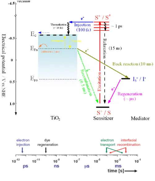
Fig. 3.2 updates the schematic to illustrate the sequence of electron transfer and charge-transport processes in the operation of the DSC. There are several main charge-separation pathways that closely mimic the photosynthesis reaction. Forward processes consist of (1) light absorption, (2) electron injection, (3) dye regeneration and (4) charge transport. The competing loss pathways are the (5) excited-state decay to ground and electron recombination with (6) dye cations and (7) oxidized redox couple. The kinetic competitions between the forward and loss pathways are critical to the DSC performance and energy conversion efficiency.
For efficient electron injection, the first condition requires the rate of electron injection to exceed the sensitizer S* decay to S0. This entails a strong coupling of the sensitizer
LUMO orbital to the metal oxide conduction states with a substantiate free energy difference to drive the reaction. Typical rates of sensitizer excited-state decay to ground are in the range 107 – 1010 s-1. DSC charge injection rates comprising nanocrystalline films of TiO2, SnO2 and ZnO have demonstrated rates greater than 1012 s-1.
Time-resolved photocurrent and photovoltage measurements and modeling studies indicate that photogenerated electrons undergo many trapping-detrapping events
repeatedly as they undertake a random walk through the film by diffusion. Under full sunlight, an average injected electron may experience a million trapping events before either percolating to the collecting electrode or recombining predominantly with an oxidizing species in the electrolyte. The dynamics is strongly influenced by the position of the TiO2 electron Fermi level: as the ∆E (= EC - EFn) becomes smaller, trap filling
increases. Typical transit times under solar irradiation are on the order of milliseconds.
Yet despite the extremely slow nature of such trap-mediated charge transport, electron collection remains favored over recombination because of the even slower multi-electron kinetics of I3- reduction on oxide surfaces. This recombination reaction has been shown to
be strongly dependently on the electron density in the TiO2 electrode and spatial
separation of the S* HOMO orbital from the metal oxide surface. The multi-electron charge-recombination reaction (Eqn. 3.1) proceeds via one or more intermediate states with a significant activation barrier. Thus similar to quantum tunneling, the rate constant decays exponentially with distance.
3 2 3
I−+ e− I−
(3.1)
Another prerequisite is a fast sensitizer regeneration which is dependent on the electrolyte ionic concentration, viscosity and the sensitizer structure. In pure solvent, the lifetime of the dye cation is on the order of milliseconds. By introducing the I-/I3- redox system in the
electrolyte, dye cation regeneration is improved significantly down to microseconds. For instance, the regeneration time in the N719 Ru-sensitizer dye in a low-viscosity electrolyte such as acetonitrile has a half-time of 1 μs which is sufficiently fast to attain unity quantum efficiency.
The forward and back reaction pathways dynamic competition may be analyzed in terms of an effective diffusion length Ln given as
n eff
L = D τ (3.2)
where Deff is the effective electron diffusion length and τ is the electron lifetime due to the
diffusion coefficients (Dn ≤ 10–4 cm2 s–1), the diffusion transit time for electrons in a
typical 10 μm thick TiO2 film is on the order of milliseconds at AM1.5 illumination.
A detailed analysis of the kinetic models and associated rate equations can be found in Ref. [6] by Zheng.
Figure 3.2 State diagram representation of the reaction kinetics in the DSC (top) and the
corresponding timescale (bottom).[6] Forward processes consist of (1) light absorption, (2)
electron injection, (3) dye regeneration and (4) charge transport. The competing loss pathways are the (5) excited-state decay to ground and electron recombination with (6) dye cations and (7) oxidized redox couple.
3.3 DSC Materials Selection
In the earlier section, it has been accentuated time and time again that the interfaces of the various chemical species are of critical importance to the conversion efficiency of the device. The kinetics of the interfacial electron-transfer dynamics is highly dependent to the energetics of the TiO2/sensitizer/electrolyte interface and the density of the states (or
Fermi Level) in the metal oxide nanocrystalline film. Thus, a modulation of the energetic and dynamic parameters is necessary to achieve optimum performance of the DSC.
The innovation in the O’Regan and Grätzel Nature article was the application of a mesoscopic film to increase the roughness and internal surface area with a newly developed trimeric ruthenium complex charge-transfer dye to achieve a high AM1.5 light-to-electricity energy conversion of over 7%.[35] The TiO2 semiconductor film was
prepared by a sol-gel process with an average particle size of 15 nm interconnected together. For a 10 μm thick nanocrystalline film, it could potentially increase the surface area by 2000-fold in contrast to a smooth flat film of an equivalent thickness. Majority of the solar irradiance consist of visible and infra-red spectra as observed in Fig. 3.3. With the trimeric ruthenium complex RuL2(μ-(CN)Ru(CN)L2')2, where L is 2,2'
bipyridine-4,4'-dicarboxylic acid and L' is 2,2'-bipyridine, the adsorption onset is shifted to 750 nm and LHE is improved up to 46%. In the following section, we would briefly review the past and current progress by different research groups that aim to improve the overall performance and stability of the DSC.
(a) (b)
Figure 3.3 (a) AM1.5 solar spectral irradiance.[38] (b) Absorption and photocurrent action specta
of bare TiO2 film and the same film coated with a monolayer of RuL2(μ-(CN)Ru(CN)L2')2 dye
sensitizer supported on conducting glass.[35]
3.3.1 Equivalent Circuit for DSCs
An equivalent circuit could be a useful tool to help researchers analyze and design improvements to the DSC device performance. Han et al.[39] used electrochemical impedance spectroscopy (EIS) to investigate and establish four internal resistance elements present in the DSCs: (1) charge transfer processes at the Pt counter electrode R1,
(2) charge transportation at the TiO2/dye/electrolyte interface R2, (3) Nernstian diffusion
in the electrolyte R3, and (4) TCO sheet resistance Rh. These measurements were carried
out on DSC specimens with a thickness 12 μm coated with a Ru N3 dye and I-/I3
-electrolyte in acetonitrile. The diode resistance R2 is found to obey the ideal diode
current-voltage characteristics represented by
2 1 exp B qV R nk T ⎛ ⎞ ∝ ⎜ ⎟ ⎝ ⎠ where q, V, n, kB and T are the elementary charge, applied bias, ideality factor, Boltzmann constant and temperature, respectively. The series resistance is equivalent to the sum of Rh, R1 and R3.
Hence, the proposed DSC electrical equivalent circuit comprises a diode R2, a series
resistance RS (= R1 + R3 + Rh) of 2.3 Ω cm2, a shunt resistance RSh of 2 kΩ/cm2 and
capacitance elements of C1 and C2 as depicted in Fig. 3.4. The thickness of the TiO2
electrode does not affect the internal resistance in the DSC.
(a) (b)
Figure 3.4 (a) Electrochemical impedance spectrum of a DSC.[39] The three semicircular shapes
are assigned to impedances related to charge transport at the Pt counter electrode (Z1) in the
high-frequency region, at the TiO2 /dye/electrolyte interface (Z2) in the middle-frequency region, and
in Nernstian diffusion within the electrolyte (Z3) in the low-frequency region, respectively. Rh is
defined as a resistance in the high-frequency range over 106 Hz. (b) Equivalent circuit based on
the I –V characteristics of DSCs.[39] C
1 and C2 are capacitance elements of Z1 and Z2, respectively.
Han et al. seeked to improve the efficiency index by reducing the series resistance elements based on the equivalent circuit model.[40] From their previous work,[39] R1 is
found to be inversely proportional to the roughness factor (RF) of the Pt electrode where RF is defined the ratio of an actual surface and the effective are to the projected area of the electrodes. As the roughness of the counter-electrode increases (by 8.9%), R1
decreases and the energy conversion efficiency η conversely increases with a higher JSC
(by 10%) in the cell. Another enhancement method is by setting the counter-electrode as close to the TiO2 anode as possible to reduce the electrolyte layer thickness and in turn,
R3. The third resistance element Rh could also be potentially reduced by decreasing the
sheet resistance in the TCO. However, transmittance of the incident light suffered and leads to an overall decrease in the device performance. Thus an optimum TCO sheet resistance of 10 Ω sq-1 (and Rh = 1.0 Ω cm2) is required to maintain a transmittance of
over 80% in the visible spectral region. By optimizing the electrolyte thickness and roughness on the counter electrode (with a TCO sheet resistance 10 Ω sq-1), the total
Light intensity is also observed to affect the series resistance in the DSC cell.[43] Even as the photocurrent improves with increasing light intensity, the fill factor for the solar cell is observed to decrease as the series resistance RS rises. This leads to an overall reduction
of the energy conversion efficiency η despite an increase of JSC and VOC with increasing
light intensity. Another possible explanation for the lowering of efficiency is attributed to the rate limitation of ionic transport and catalytically activated redox reaction on the electrode. It is also noted that increasing the semiconductor metal oxide electrode thickness would increase the RS. More importantly, the critical point regarding increasing
the film thickness is the associated increase of recombination reaction during the electron transfer process in the electrode.[47]
3.3.2 Wide Energy Bandgap Semiconductor Materials for Electrode
The heart of the DSC operation is for the sensitizer monolayer affixed on the semiconductor electrode to absorb the incident light, generate excitons and inject the electrons into the conduction band of the mesoporous nanocrystalline film. A wide energy bandgap material is necessary for the electrode to remain transparent to infra-red and visible spectra for photon absorption by the sensitizer molecule.[41] A variety of common wide energy bandgap semiconductors have been reviewed,[42,43] however, anatase TiO2 is the most widely preferred. Nb2O5 shows the next highest IPCE to TiO2
and the highest VOC among the other (ZnO, SnO2, WO3, Ta2O5, ZrO2 and In2O3)
candidates when coated with Ru (II) cis-bis-(thiocyanato)bis(2,2'-bipyridyl-4,4'-dicarboxylic acid) complex sensitizer.[42] This is attributed to the strong interface coupling between the delocalised π* state of the Ru-complex ligand and d-orbitals of the TiO2 and Nb2O5 conduction bands which serve as the charge carrier pathway for
extremely fast electron injection efficiency. VOC is defined as the difference between the
I-/I3- redox potential and the semiconductor conduction band as depicted in Fig. 3.2. Thus,
VOC and the photovoltage increases with more negative potentials of the conduction
band.[43] However, this will also lead to a lower free energy driving force for charge separation and a lower quantum efficiency for charge generation and JSC output.[36]
A simple modification to TiO2 nanocrystalline film by adding a 1 - 2 nm thin Al2O3 or
Nb2O5 barrier layer significantly inhibits the recombination rate with the oxidized redox
couple in the electrolyte and increases the VOC, JSC and FF and overall energy conversion
efficiency η up to 35%.[44-45] Studies have also demonstrated that only highly basic metal oxide layers such as Al2O3 can deprotonate the TiO2 surface and reduce the overall
dependence of the electron density and recombination dynamics at the interface.[46] The barrier layer increases the physical separation between the injected electrons and the I-/I3
-redox system in the electrolyte, but it should also be sufficiently thin to maintain the high tunneling efficiency of the electrons from the sensitizer molecules into the semiconductor interconnected network.
3.3.3 Photosensitizers
The most successful sensitizers are the ruthenium bipyridyle complex dyes commonly known as the N3 dye [ruthenium complex cis-RuL2(NCS)2] and the black dye
[tri(cyanato)-2,2′2′′-terpyridyl-4,4′4′′-tricarboxylate)Ru(II)] illustrated in Fig. 3.5.[36,47] The absorption spectrum of a fully protonated N3 has maxima at 518 and 380 nm and extinction coefficients of 1.3 × 10⁴ and 1.33 × 10⁴ M–1 cm–1, respectively. In addition, the complex has an emission wavelength of 750 nm with an excited-state lifetime of 60 ns. Compared to the N3, the black dye extends the response to the incident irradiance by another 100 nm into the infra-red spectrum with the photocurrent onset close to 920 nm. Currently, the highest certified DSC conversion efficiency of 11.1% was demonstrated using the black dye.[15] Most information on the dye sensitizers can be found in Ref. [36]. New Ru-sensitizers such as K-19, Z-907 and Z-910 with improved light harvesting, excellent yield and enhanced thermal stability have also been recently reported.[59-62,92]
(a)
(b)
Figure 3.5 (a) Chemical representation[48] and spectral response curve of the photocurrent[49] for
the DSC sensitized by N3 and the black dye. (b) Room-temperature optical absorption spectra of a dispersion of 3 nm MPA-capped CdSe QDs in methanol and a 2μm long ZnO nanowire-coated FTO substrate before and after adsorption with the same QDs, and IPCE and LHE values.[55]
Sensitized solar cells utilizing semiconductor nanocrystals or quantum dots[50-52] (QDs) as photosensitizers in place of Ru dyes have also been demonstrated in recent years. Compound semiconductor QDs of III-V and II-VI with suitable bandgaps between 1.0 eV to 2.7 eV due to nanocrystal size and components are excellent candidates.[47] The properties of QDs arise from considerations of quantum mechanics and Heisenberg’s uncertainty principle.[52] In general, as the electron gets more closely confined, the momentum becomes more uncertain and translates to a higher average energy. 3D quantum confinement gives rise to complete localization of electrons and holes and a discrete spectrum of δ-function-like density of states resulting from the geometric confinement of bound electron-hole pairs or excitons. The length scale of the bound oppositely-charged carrier pair in a bulk material is expressed as an exciton Bohr radius. Thus, when the electron-hole pair is confined in a nanocrystal with dimensions approaching the bulk exciton Bohr radius, the effective bandgap of the semiconductor increases. The smaller the nanocrystal, the larger the effective bandgap, and the greater the energy of the optical emission resulting from electron-hole recombination. Typical exciton Bohr radius for II-VI semiconductors range from 2.2 nm for ZnS to 7.5 nm for CdTe, and from 11 nm (InP) to 60 nm (InSb) for III-V semiconductors.[53] Quantum dot solar cells could have theoretical efficiencies in excess of over 50%.[8]
Leschkies et al.[55] attached CdSe QDs with sizes ranging from 3 to 4 nm onto ZnO nanowires with lengths and diameters between 2 and 12 μm and 75 and 125 nm, respectively. Mercaptopropionic acid (MPA) is used as the linker between the QD and ZnO interface, where the sulfur atom in MPA is bounded to the QDs and the carboxylic acid group links to the nanowires. CdSe QDs absorb photons between 400 to 600 nm with a maximum IPCE output of 15% at 450 nm as shown in Fig. 3.5. Under illumination, electron-hole pairs are formed in the QDs and the electrons are injected into ZnO via quantum tunneling mechanism. The photoexcited electrons in the CdSe QD lie above the ZnO conduction band edge, and transfer into ZnO at the heterojunction interface to lower the energy state. However, the nanowire solar cell architecture has a lower LHE and sensitized surface area coverage compared to the Ru-dye sensititzed TiO2 mesoporous
redox couple electrolyte environment accelerates the corrosion of the compound semiconductor nanocrystals. Oxygen plasma treatment was found to enhance the QD adsorption on the surface and improve the overall conversion efficiency of the CdSe-QD- sensitized ZnO-nanowire photovoltaic cells as the JSC enhances by more than an order of
magnitude. CdSe QD sensistized cells assembled with 12 μm long plasma-treated ZnO nanowires have JSC ranging from 1 to 2 mA cm-2 and VOC of 0.5-0.6 V with a FF of ~ 0.3
that is equivalent to 0.36% AM1.5 efficiency.
Despite these negative aspects in QD DSC prototypes, carrier multiplication in nanocrystalline quantum dots could lead to substantial improvements in the performance of solar cells technologies.[56] Moreover, the absorption spectrum of the QD is continuous from the onset of the first excitonic peak to higher energy side which improves the absorption wavelength range. Thus, QD solar cells in theory would increase the relative efficiency of single-layer photovoltaic and photochemical solar cells by about 50%.[8,57] Manufacturing cost for solar cells is expected to be reduced as QDs could be fabricated cheaply with solution-based colloidal synthesis methods[51] and efficient quantum dot solar cells may not require multilayered construction [57].
3.3.4 Electrolytes
In 2004, AISEN and Toyota performed outdoor durability evaluation of N3-sensitized DSC modules consisting of 10 cm × 10 cm in cell size in (I-/I
3-) methoxypropionitrile
liquid electrolyte for half a year to verify the outdoor stability and higher performance over conventional silicon solar cells.[58] One of the main observations from the outdoor assessment is the leakage of the liquid electrolyte in one of the four modules. Other possible performance limiting parameters are the possible desorption of loosely attached dyes, photodegradation of the desorbed state, as well as, corrosion of the Pt counterelectrode by the I-/I3- redox couple.[59] A possible measure to prevent leakage
issues is to a form of quasi-solid electrolyte via polymeric gelation of the ionic liquid solvent.[59,60] Wang et al.[60] uses a photochemically stable fluorine polymer
methoxypropionitrile (MPN)-based liquid electrolyte. The gel electrolyte penetrates into the TiO2 mesoporous network in the liquid phase above TSG and solidifies at a lower
temperature. Despite the hardening of the electrolyte into a quasi-solid form, the gel-electrolyte retains impressive conductivity values as the I-/I3- redox couple ions continue
to diffuse freely within the liquid domains entrapped within the three-dimensional gel network. Coupling the gel electrolyte with the amphiphilic Z-907 Ru dye, thermal stability is enhanced as the device efficiency performance maintains above AM1.5 efficiency of 6% with no significant degradation under sustained heating of 80 °C for 1000 hours.[59] The alkyl side chains of the Z-907 dye is hydrophobic in nature and reduce the dye solubility within the liquid domains in the quasi-solid electrolyte network. This in turn minimizes desorption of the dye molecules from the TiO2 film surface and
enhance thermal stability.Wang et al. reported the pairing of a new K-19 amphiphilic sensitizer [Ru(4,4'-dicarboxylic acid-2,2'-bipyridine) (4,4'-bis(p-hexyloxystyryl)-2,2'-bipyridine)×(NCS)2] with 1-decylphosphnic acid (DAP) as a coadsorbant into
MPN-based electrolyte to reduce the volatility and achieve more than 8% energy conversion efficiency with superior thermal stable properties.[62] An alternative gelation procedure makes use of silica spheres to gel MPII-base ionic electrolytes.[61]
Another design to overcome possible liquid electrolyte leakage in photoelectrochemical cells is the use of p-type organic conductor such as the spiro-OMeTAD to form a complete solid dye-sensitized solar cell (SSC).[63] Spiro-OMeTAD has a work function
of 4.9 eV and hole mobility of 2 × 10⁻⁴ cm2 s-1.[36] However, such solar cells have several disadvantages. Firstly, the SSC suffers from a fast interfacial electron-hole recombination and decreases the electron diffusion length to just a few microns. It is also hard to achieve an optimum filling of the solid hole conductor within the mesoporous TiO2
network. However, this impediment may be overcome by employing ordered perpendicularly aligned oxide films with regular mesoporous channels for easy filling. Recently, a 8 μm thick TiO2 nanocrystalline film solar cell coated with a thin barrier layer
of Al2O3 in I2/NaI doped solid-state polymer electrolyte built on flexible substrates
3.4 Nanoarchitectures for DSCs
While the mesoporous TiO2 nanocrystalline film enhances the effective surface area for
dye sensitizer molecule attachment for light absorption, one particular weakness is the presence of a massive number of interfacial boundaries acting as trap sites for electron transport. A trap-limited diffusion model has been verified in numerical simulations and experimental data that causes lossy electron transport and lowers overall efficiency of the cell. Another flaw that works against the notion of large metal oxide surface area is the presence of interfaces exposed to the electrolyte. These exposed surfaces, which are not anchored with dye molecules would be in direct contact with electrolyte and provide new recombination pathways as electrons are lost to the I-/I3- redox couple when percolating
through the network. A thicker film electrode also leads to resistance loss and overall reduction in the fill factor and photovoltage. To counter this weakness, an optimal thickness of TiO2 nanoparticle film (within the electron diffusion length dimension) is
deposited for maximum energy conversion efficiency.
3.4.1 Nanowire and Nanotube DSCs
The one-dimensional nanowire electrode architecture provides a possible way to tackle the electron percolation deficiency in a nanocrystalline film by providing a more direct path, with less trap sites, for electron transport to the collection electrode. By replacing the nanoparticle structure with an array of single crystalline ZnO nanowires,[65] electron diffusion length and thus lifetime were shown to improve by several orders of magnitude over a random nanoparticle network. Moreover, the nanowires introduce an internal electric field to provide additional driving force for charge separation from the dye molecule into the ZnO electrode. The nanowires can also scatter light and enhance the light harvesting efficiency. From the measurements, the electron diffusitivity coefficient is calculated to be 0.05 – 0.5 cm2 s-1 which is much higher than the reported diffusitivity
measurement of 1.7 × 10⁻⁴ cm2 s-1 in ZnO nanocrystalline film.[65,66] The most attractive
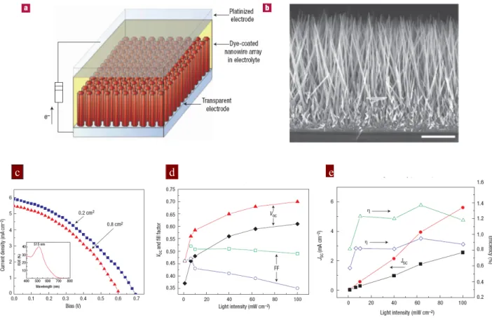
aspect of this work is the use of solution-based processing to form single crystalline nanowires with aspect ratio above 125. Fig. 3.6 illustrates the schematic diagram of the ZnO wire array DSC.[65]
c d e
Figure 3.6 (a) Schematic diagram of the ZnO nanowire DSC. Light is incident through the
bottom electrode. (b) SEM cross-sectional micrograph of a cleaved nanowire array on FTO. The wires are in direct contact with the substrate, with no intervening particle layer. Scale bar, 5 μm. (c) Traces of current density against voltage (J–V) for two cells with roughness factors of ~200. The small cell (0.2 cm2) shows a higher V
OC and JSC than the large cell (0.8 cm2). The fill factor
and efficiency are 0.37 and 1.51% and 0.38 and 1.26%, respectively. Inset, the external quantum efficiency against wavelength for the large cell. (d) Open-circuit voltage and fill factor against light intensity, and (e) short-circuit current density and efficiency against light intensity for cells with roughness factors from 75 to 200.
For AM1.5 sun irradiance, the best performing cells have JSC = 5.3–5.85 mA cm–2, VOC =
0.61–0.71 V, FF = 0.36–0.38 and efficiency η = 1.2–1.5% with N719 dye and standard I -/I3- redox couple electrolyte. IPCE near the absorption peaks record only 40-43% due to
the low dye loading on the nanowire films. The relatively low conversion efficiency of 1% is due to the lower surface to volume ratio of the nanowire compared to the nanoparticle film geometry. Another reason is attributed to a lower electron injection efficiency of dye molecule to ZnO. In general, TiO2 is commonly recognized as the more
Another alternative ordered DSC architecture consists of TiO2 nanotube arrays prepared
by a 250 μm titanium thin film anodic oxidation on a FTO substrate.[67] The typical nanotubes have pore size of 46 nm and wall thickness of 17 nm. The length scale is limited to 360 nm due to limitation of the starting high quality titanium film thickness at 500 nm. To create additional N719 dye loading area, the nanotube array films underwent further TiCl4 chemical treatment. Similar to its nanowire cousin, the transparent
nanotubes exhibit highly directional charge transport characteristics with fewer interfacial recombination traps. The TiCl4-treated 360-nm-thick nanotube array DSCs exhibit a JSC
of 7.87 mA/cm2, a VOC of 0.75 V, and a FF of 0.49, with an overall conversion efficiency
of 2.9%.
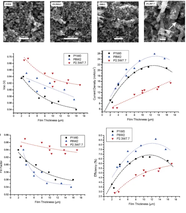
Sub-micron TiO2 nanoparticles (400 nm) have been incorporated into the nanoparticle
film DSC as scattering centers to increase the IPCE and JSC and achieve a maximum
certified efficiency of 11.1%.[15] The same principle is likewise applied in a nanoparticle/nanowire composite hybrid DSC to take advantage of the rapid electron transport rate and light scattering effects in the nanowires.[68] Fig. 3.7 shows the performance of the composite DSCs as a function of nanowires and film thickness. In general, the most efficient hybrid DSC consists of 0.8 nanoparticle and 0.2 nanowire weight concentration ratio with η = 8.6% under AM1.5 illumination. This cell composite composition maximizes the light scattering, rapid electron transport rate and reduced recombination effects largely due to the nanowire counterparts and the large surface area for photon harvesting by the N719 dyes molecules attached on the nanoparticle surfaces. However, with an increasing concentration in the composite cell, the nanowires become the dominant phase and result in the fall of efficiency due to lower dye loading area.

![Table 2.2 Notable exceptions of confirmed cells and module results. [20]](https://thumb-eu.123doks.com/thumbv2/123doknet/14384365.506954/23.918.131.797.321.676/table-notable-exceptions-confirmed-cells-module-results.webp)
![Figure 3.4 (a) Electrochemical impedance spectrum of a DSC. [39] The three semicircular shapes are assigned to impedances related to charge transport at the Pt counter electrode (Z 1 ) in the high-frequency region, at the TiO 2 /dye/electrolyte interfa](https://thumb-eu.123doks.com/thumbv2/123doknet/14384365.506954/31.918.140.784.197.445/electrochemical-impedance-semicircular-impedances-transport-electrode-frequency-electrolyte.webp)