HAL Id: hal-01225356
https://hal.archives-ouvertes.fr/hal-01225356
Submitted on 6 Nov 2015
HAL is a multi-disciplinary open access
archive for the deposit and dissemination of
sci-entific research documents, whether they are
pub-lished or not. The documents may come from
teaching and research institutions in France or
abroad, or from public or private research centers.
L’archive ouverte pluridisciplinaire HAL, est
destinée au dépôt et à la diffusion de documents
scientifiques de niveau recherche, publiés ou non,
émanant des établissements d’enseignement et de
recherche français ou étrangers, des laboratoires
publics ou privés.
Enhancement of the Spatial Resolution of Near-Field
Immunity Maps
Alexandre Boyer, Manuel Cavarroc
To cite this version:
Alexandre Boyer, Manuel Cavarroc. Enhancement of the Spatial Resolution of Near-Field Immunity
Maps. 10th International Workshop on the Electromagnetic Compatibility of Integrated Circuits
(EMC Compo 2015), Nov 2015, Edimburgh, United Kingdom. 6p. �hal-01225356�
Enhancement of the Spatial Resolution of Near-Field
Immunity Maps
A. Boyer, M. Cavarroc
CNRS, LAAS, 7 avenue du colonel Roche, F-31400 Toulouse, France Univ. de Toulouse, INSA, LAAS, F-31400 Toulouse, France
Contact: alexandre.boyer@laas.fr Abstract—Near-field injection is a promising method for the
analysis of the susceptibility of electronic boards and circuits. The resulting immunity map provides a precise localization of the sensitive area to electromagnetic disturbances. A major requirement is the spatial resolution of the immunity map, which depends on the size of the injection probe and the separation distance between the probe and the device under test. This paper aims at proposing a post-processing method to enhance the spatial resolution of immunity map and validating it on case studies at board and integrated circuit levels.
Keywords— Near-Field Scan; Immunity; Resolution enhancement; Plane Wave Spectrum Theory.
I. INTRODUCTION
Near-field scan is a well-established method for the diagnosis of EMC problems at printed circuit board (PCB) and integrated circuit (IC) package levels. It consists in measuring the local electric or magnetic fields created above PCB traces and ICs with a miniature receiving probe for a root-cause analysis of emission issues. The method can be reversed to apply local electromagnetic disturbances and is known as near-field injection. A near-field probe is placed in the vicinity of an electronic device and excited by a disturbance signal in order to induce a local intense electric or magnetic field. The coupling of the field may induce enough large voltage fluctuations across a PCB or an IC under test to trigger failures [1] - [5]. Both methods provide 2D cartography or map of the local emission (emission map) or amplitude of the failure induced by the probe according to its position (immunity map).
The quality of the diagnosis made with these methods is dependent on the spatial resolution of the cartography, i.e. the ability to locate the source of a near-field emission or the coupling area with a sufficient accuracy. The resolution depends on the distance between the probe and the circuit under test but also on the dimensions of the probe. Due to its finite size, the probe produces a significant field over a relatively large volume which couples over a relatively large area of the device under test (DUT). Huge efforts are done to reduce near-field probe dimensions and thus improve the spatial resolution. However, the main drawback of the miniaturization is either the degradation of receiving probe sensitivity, or the reduction of the field produced by the injection probe. Recently, numerous research works have been led to improve the resolution of emission cartography by post-processing methods. They consist in compensating the
receiving characteristic of the measurement probe. Three types of method have been proposed: plane wave spectrum (PWS) theory [6] [7], image restoration techniques based on Wiener filtering [8] [9] and Neural network based post-processing [10]. The resolution of emission scan are considerably improved even when the measurement is done with large receiving probes.
However, this type of post-processing methods has never been used to improve the resolution of immunity scan. Contrary to emission scan post-processing, the objective is not to compensate the receiving characteristics of the measurement probe and extract the actual undisturbed field distribution. The main purpose is to extract the receiving characteristic of the device under test, in order to improve the localization of coupling area to near-field disturbances produced by a large injection probe. This paper proposes to reuse PWS theory in order to improve the resolution of immunity scan, and demonstrate its validity on practical case studies at PCB and IC levels. After a description of the method, the injection probe emission profile which is necessary to the method is extracted. Although this post-processing method can be applied either on electric or magnetic field injection, previous studies such as [14] have demonstrated experimentally the better resolution and injection efficiency of magnetic field probe. For this reason, the method is applied only on magnetic field injection in this paper. In a fourth part, the method is applied on simple PCB traces. In the fifth part, the method is applied at IC level in order to improve the identification of package pin and die part responsible of the disturbance coupling.
II. THEORETICAL BACKGROUND
Let consider a near-field injection probe excited by a sinusoidal signal which produces a field F(xs,ys,zs) in any point. The field is supposed known and undisturbed by nearby objects. For near-field injection on PCB or IC, we are only concerned by the distribution of the field F on a 2D horizontal plane (xs,ys) placed at a constant distance or scan altitude hs below the injection probe (Fig. 1). This 2D distribution is called the spatial profile of the field F. The result of a near-field injection scan on a PCB or IC is a 2D immunity map which provides for each probe position (xp, yp) placed at the scan altitude hs above the DUT its response S to the near-field disturbance produced by the probe (Fig. 1). The immunity map provides an indirect and distorted picture of the coupling
area of the incoming disturbance, because the probe produces a significant field over a large surface of the DUT.
xs ys zs OS Near-field probe hS
Field emitted by the probe at position (xs,ys,-hs) 2D distribution of field F xp yp zp O DUT hS Immunity 2D map S(xp,yp,zp)
Response S of the DUT when the probe is located
in (xp,yp,-hs)
Near-field probe
Fig. 1. Spatial profile of the field F produced by the probe at a scan altitude -hS (top), immunity map of the DUT (bottom)
The spatial profile of the DUT response S is related to the field F by a DUT property called the receiving characteristic R. The relation is given by equation 1. The receiving characteristic of the DUT quantifies the response of the DUT to one particular component of the field F produced by the injection probe placed in (xp,yp,-hs). Thus, the spatial profile of the receiving characteristic of the DUT provides a direct information about the coupling area and the sensitivity of the DUT to the disturbances produced by the near-field injection probe.
(
)
(
)
(
p s p s)
(
s s)
s s p p p pdy
dx
y
x
F
y
y
x
x
R
y
x
F
R
y
x
S
∫∫
−
−
=
∗
=
,
,
,
,
(1)The determination of the DUT receiving characteristic is easier in spectral domain than spatial domain representation. The transformation is based on the PWS theory. It consists in decomposing the field into a superposition of an infinite number of plane waves propagating in x and y directions with wave numbers kx and ky. The relation between spatial and spectral domain representations of the field is ensured by a 2D Fourier transform in the xy plane, as given by (2) and (3) where subscript F~denotes the spectral domain representation.
(
)
∫ ∫
+∞(
)
∞ − − −=
F
x
y
z
e
e
e
dxdy
z
k
k
F
~
x,
y,
,
,
jωt jkxx jkyy (2)(
)
=∫ ∫
−+∞∞(
)
x y y jk x jk t j y x k ze e e dk dk k F z y x F ω x yπ
, , ~ 4 1 , , 2 (3)With the spectral domain representation, (1) is rewritten in the following form. The receiving characteristic is the ratio between the DUT response and the field emitted by the probe.
(
) (
(
)
)
z
k
k
F
z
k
k
S
z
k
k
R
y x y x y x,
,
~
,
,
~
,
,
~
=
(4)It should be noted that the field, the DUT response and the receiving characteristic are complex figures. The extraction of the receiving characteristic requires the measurement of the phase of the field and the DUT response. Basically, the extraction of the receiving characteristic procedure consists in five steps:
1. Acquire the immunity map of the DUT S(xp,yp,-hs) with a given injection probe
2. Obtain the spatial profile of the field produced by the injection probe F(x,y)
3. Compute S~ and F~ by a 2D FFT 4. Compute R~ according to (4) 5. Compute R by inverse 2D FFT.
In practice, various sources of errors degrade the accuracy of this method. First, the result is affected by systematic errors on probe positioning, measured or simulated spatial profiles of disturbing field and DUT response. Secondly, the result is sensitive to measurement noise. To reduce the random noise influence, the noisy wave number components, i.e. with an amplitude less than an arbitrary signal-to-noise ratio constraint, are filtered out. Thirdly, as the number of spatial samples is finite, truncation errors affect the FFT results. The induced oscillations (Gibbs effect) may be reduced by applying windowing such as Blackman window. Finally, if the influence of the DUT on the injection probe characteristics is not negligible, the spatial profile of the field produced by the injection probe may become erroneous.
III. EXTRACTION OF THE SPATIAL PROFILE OF MAGNETIC
FIELD EMITTED BY THE INJECTION PROBE
In the following part, the proposed method will be validated on test structures which couple mainly the tangential component of the magnetic field. The cross-polarization to other H field components are neglected. Beforehand, it is necessary to obtain the spatial distribution of the tangential magnetic field produced by the injection probe.
A. Presentation of the injection probe
The injection probe used in this study is described in Fig. 2. It consists in a handmade 3 turns coil built on a semi-rigid coaxial cable. It produces an important tangential magnetic field in its vicinity. Increasing the number of turns enhances the magnetic field produced by the probe but degrades the resolution of the resulting immunity map.
1.3 mm
2.7 mm
0.4 mm
1.04 mm
B. Simulation of the magnetic field emitted by the injection probe
The H field spatial profile produced by the injection probe can be obtained either by measurements or simulations. The advantage of the simulation is that the result is obtained rapidly and is noise-free. A model of the injection probe is built and simulated with FEKO according to the Methods of Moments [11]. However, measurements may be necessary to confirm the validity of the simulation results.
In order to verify the relevance of simulation results, the measurement calibration described in Fig. 3 is performed. It consists in measuring the coupling coefficient S21 between the injection probe and a calibrated measurement probe with a known receiving characteristic. The receiving probe is displaced on a 2D horizontal surface at the scan altitude hs below the injection probe. The measurements are done between 10 MHz and 1 GHz for scan altitude ranging between 0.5 and 2 mm. The measurement probe is a miniature magnetic field probe which has been characterized previously in order to compensate its receiving characteristic according to the method described in [6] or [7]. If the measurement probe is small enough to be considered as punctual, its receiving characteristic is given by its performance factor PF. The relation between the tangential magnetic Htan field emitted by the injection probe and the measured coupling coefficient is given by (5). x y z hS Injection probe O Calibrated measurement probe Vector Network Analyzer Port 1 Port 2 + 1 V Scan step = 0.25 mm
Fig. 3. Measurement of the field spatial profile produced by an injection probe
(
−
)
=
−
(
( )
−
)
+ 1 21 tan,
,
,
,
,
,
V
f
PF
f
h
y
x
S
j
f
h
y
x
H
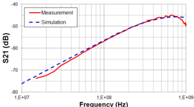
S S (5)where f is the frequency and V1+ the amplitude of the forward wave which excites the injection probe. Fig. 4 shows a comparison between measurement and simulation of the coupling coefficient S21 between both probes when they are separated by 1 mm. Measurements and simulations are in very good accordance up to 800 MHz. Discrepancies above 800 MHz may be due to coaxial-wire transitions which are not modeled.
Fig. 4. Comparison between simulated and measured coupling between emitting and receiving probe
Fig. 5 compares the measured and simulated profile of the tangential magnetic field profile emitted by the injection probe along the X axis for hs = 1 mm. The injection probe is excited by a 400 MHz sinusoidal signal with an amplitude of 1 V. The measured profile is affected by noise and the windowing effects at the scan region edges introduced by the probe compensation method. Moreover, the measured profile is not perfectly symmetrical because of probe mounting and positioning errors. However, measured and simulated field profiles are in good accordance. It confirms the relevance of electromagnetic full-wave simulation to provide the spatial profile of the near-field emission of the injection probe. In the next part, the spatial profile of the magnetic field emitted by the injection probe will be obtained by simulation.
Fig. 5. Comparison between simulated and measured H field emitted by the H field injection probe
IV. VALIDATION OF THE METHOD ON PCBTRACES
A. Description of the test structures
Several basic PCB traces have been designed to validate the proposed method. The following table describes the test structures. The experimental set-up described in Fig. 6 is used to measure the coupling coefficient between the injection probe and the line under test, according to the probe position above the line. The voltage induced on the tested line is deduced from the coupling coefficient. From the spatial profiles of the simulated magnetic field emitted by the injection probe and the coupled voltage on the tested lines, the receiving characteristic of the line is extracted according to the method presented in part II. The results presented in the
following parts have been obtained with harmonic injection at 400 MHz and a scan altitude hs = 1 mm.
TABLE I. DESCRIPTION OF THE PCB LINES UNDER TEST
Designation Description
Narrow microstrip line
50 Ω microstrip line, width = 0.15 mm, length = 50 mm
Coupled-edge microstrip line
Two microstrip lines separated by 1 mm, width = 0.15 mm, length = 50 mm x y z hS Injection probe O
Line under test
Vector Network Analyzer Port 1 Port 2 + 1 V Scan step = 0.25 mm PCB 50 Ω
Fig. 6. Measurement of the coupling between the injection probe and a PCB trace
B. Results
Firstly, the receiving characteristic of a narrow microstrip line is extracted from the measurement and compared with simulation. The receiving characteristic of the microstrip line is dependent on its width, the distance to the reference plane, and its length. Fig. 7 shows that measured and simulated receiving characteristics are in good accordance, proving the validity of the measurement method on this simple case study. A peak appears at the exact position of the microstrip line. The oscillations are due to windowing effects.
Fig. 7. Comparison between measured and simulated receiving characteristics of a narrow microstrip line
In order to highlight that the receiving characteristic profile offers a better resolution than the typical immunity map, the spatial profiles of the voltage induced on the line under test and its receiving characteristic are compared, as shown in Fig. 8. Their values are normalized to simplify the comparison. ? The voltage or the receiving characteristic profiles are divided by their respective maximum value, in order to compare different spatial profiles. Both curves present a main lobe appearing above the line under test. The
spatial resolution of both profiles is quantified according to the width at half maximum of the main lobe. The resolutions of the measured voltage and receiving characteristic profiles are equal to 2.5 and 1.25 mm respectively. The resolution of the line receiving characteristic profile is twice better than that of the induced voltage profile.
Fig. 8. Comparison between the spatial profile of voltage induced on the narrow microstrip line and its receiving characteristic
The second case study is the edge-coupled microstrip line. It aims at verifying that plotting the receiving characteristic profile facilitates the separation between two neighbor lines. Fig. 9 compares the spatial profiles of voltages induced on each line and their receiving characteristic are compared. The line receiving characteristic profile present a narrower main lobes than those observed on the induced voltage profile. The separation between both lines is improved with the receiving characteristic representation. The localization of the lines responsible of the disturbance coupling is simplified with the receiving characteristic profile.
Fig. 9. Comparison between the spatial profile of voltage induced on the edge-coupled microstrip lines and their receiving characteristics
V. VALIDATION OF THE METHOD ON INTEGRATED CIRCUIT
The previous methodology is now applied on an integrated circuit in order to improve the localization of disturbed package pins or circuit interconnects. The experiments are performed on a test-chip described below.
A. Description of the test structures
A test chip has been designed with Freescale® in 0.25 µm SMARTMOS 8 technology with 4 metal layers in order to study the near-field injection on basic interconnects and bus structures. Twenty four on-chip sensor (OCS) are disseminated within the test chip to reconstruct the time domain profile of the local voltage fluctuations induced by the
near-field injection. The OCS is able to measure the waveform of voltage bounces across non accessible nodes with a precise time resolution, a large bandwidth and a low intrusivity. The acquisition principle is based on a sequential equivalent-time sampling which provides a very large virtual bandwidth in spite of a limited sampling rate. Its principle is explained in [12]. In order to prevent noise coupling to sensors, they are supplied by an internal voltage regulator connected to a dedicated power supply and are isolated from the bulk and conductive substrate by a deep N-well. Moreover the OCS is routed with only three metal layers. A complete shielding of the OCS is done with the top level metal layer in order to limit the disturbance of the OCS due to near-field injection. The reader can refer to [13] for more details about the sensor design and performances.
The test chip is mounted in CQFP64 package with a removable metallic lid in order to place the near-field probe as close as possible to the die surface. Previous near-field injections have been performed on this circuit, showing a significant coupling of the tangential magnetic field component [14]. Fig. 10 presents the experimental setup in order to measure the voltage coupled to the circuit and extract its receiving characteristic. The injection probe is displaced above the test chip and excited by a sinusoidal RF source. A sensor connected on an internal interconnect terminated by 50
Ω loads is used to monitor the voltage fluctuation induced in
the circuit according to the injection probe position. The signal acquired by the OCS is then transmitted through a dedicated output to an external acquisition card and post-processed to provide the time-domain profile of the voltage measured by the sensor. Three dedicated pins are associated to the sensor: an output, a power supply and a ground reference, placed on the same side of the package.
PCB x y z hS Injection probe O
Circuit under test
+ 1 V Scan step = 0.1 mm Acquisition card RF disturbance source S y n c h ro n iz a ti o n OCS Sensor output
Fig. 10. Measurement setup of the voltage coupled on the test-chip by the injection probe
B. Experimental results
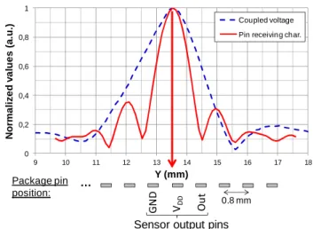
A first scan is done above the package side containing the sensor pins. The probe is excited by a sinusoidal signal with a frequency equal to 200 MHz. The probe is placed at 500 µ m above the package pins. The scan step is set to 0.11 mm. The evolution of the voltage measured by the sensor and the extracted receiving characteristic according to the probe position along the package side are compared in Fig. 11. The values are normalized for comparison purpose. The location of
sensor pins is also indicated. Coupled voltage and receiving characteristic spatial profiles present a main lobe with width half maxima equal to 2.4 and 1.2 mm respectively. The resolution of the pin receiving characteristic profile is twice better than that of the induced voltage profile. Both main lobes are centered above the package pins associated to the sensor, but the receiving characteristic profile is clearly centered on the power supply pin of the sensor. The result proves that the power supply pin is responsible of the coupling of the RF signal on the sensor at 200 MHz.
0 0,2 0,4 0,6 0,8 1 9 10 11 12 13 14 15 16 17 18 N o rm a li z e d v a lu e s ( a .u .) Y (mm) Coupled voltage Pin receiving char.
O u t VD D G N D … 0.8 mm Sensor output pins Package pin
position:
Fig. 11. Comparison between the spatial profile of voltage induced on the sensor and its receiving characteristic
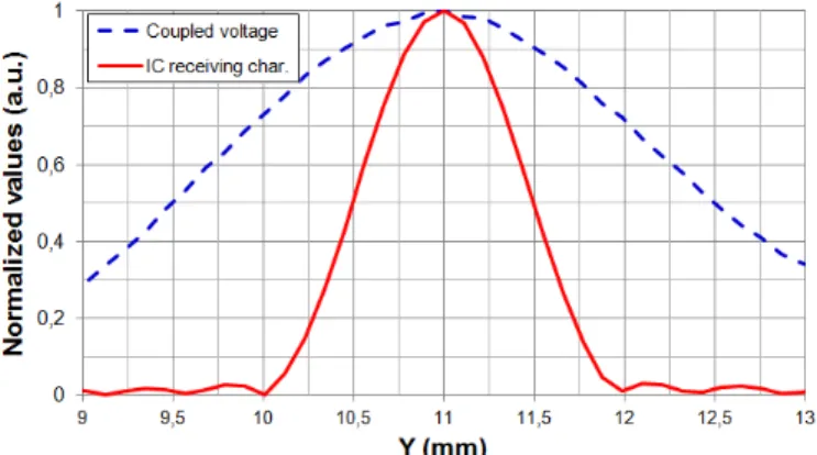
A second scan is done above one side of the die. The position of the scan and sensor bonding wires is shown in Fig. 12. The size of the probe is also reported for comparison purpose with the die surface. The probe is excited by a sinusoidal signal with a frequency equal to 200 MHz. The probe is placed at 700 µm above the die surface. The scan step is set to 0.11 mm. X (mm) Y (mm) 12 13 14 9 10 11 12 13 11
Injection probe size and orientation H field S c a n t ra je c to ry Sensor OUT sensor VDDsensor GND sensor
Fig. 12. Position of the near-field scan above the die surface
The evolution of the voltage measured by the sensor and the extracted receiving characteristic according to the probe position are compared in Fig. 13. Coupled voltage and receiving characteristic spatial profiles present a main lobe with width half maxima equal to 3 and 1 mm respectively. The
resolution of the receiving characteristic profile is three times better than that of the induced voltage profile. The main lobe of the coupled voltage profile is almost as wide as the die so that the localization of the coupling area is not precise. In contrary, the main lobe of the receiving characteristics is centered above the three bonding wires associated to the sensor. However, the resolution is not sufficient to identify clearly the bonding wire responsible of the coupling, since their separation is about 150 µm.
Fig. 13. Comparison between the spatial profile of voltage induced on the circuit under test and its receiving characteristic
VI. CONCLUSION
Near-field injection is a promising method for the analysis of the susceptibility of electronic cards and integrated circuits. The precise localization of sensitive area of a device under test depends on the spatial resolution of the immunity map resulting from the scan. This paper has shown that miniaturizing injection probe is not the only method to improve the resolution of immunity map. Applying a post-processing method to extract the receiving characteristic of the device under test offers a better spatial resolution. Examples at PCB and IC levels presented in this paper show that it may provide a two or threefold improvement of the spatial resolution. We insist that this method is not an alternative to the miniaturization of injection probe. As this miniaturization effort leads to a reduction of the produced disturbing field, it constitutes an additional method to improve the resolution of immunity map obtained with relatively large injection probe.
In this paper, the receiving characteristic has been extracted from the measurement of the voltage induced by the injection probe on the device under test. However, in practical
immunity test, the measurement of the induced voltage does not constitute the unique failure criterion. Further studies have to be led to verify that this method is applicable whatever the monitored failure criterion.
REFERENCES
[1] S. Zaky, K.G. Balmain, G.R. Dubois, “Susceptibility Mapping”, in Proc. Int. Symp. on EMC, 1992, pp. 439-442.
[2] O. Kroning, M. Krause, M. Leone, "Near field-Immunity Scan on Printed Circuit Board Level", in Proc. SPI, 2010, pp. 101-102. [3] A. Boyer, E. Sicard, S. Bendhia, « Characterization of the
Electromagnetic Susceptibility of Integrated Circuits using a Near Field Scan », Electronic Letters, vol. 43, no. 1, pp. 15-16, 4th Jan. 2007. [4] T. Dubois, S. Jarrix, A. Penarier, P. Nouvel, D. Gasquet, L. Chusseau, B.
Azaïs, " Near-Field Electromagnetic Characterization and Perturbation of Logic Circuits", IEEE Trans. on Instrumentation and Measurement, vol. 57, no. 11, pp. 2398 - 2404, Nov.2008.
[5] G. Muchaidze, J. Koo, Q. Cai, T. Li, L. Han, A. Martwick, K. Wang, J. Min, J. L. Drewniak, D. Pommerenke, "Susceptibility Scanning as a Failure Analysis Tool for System-Level Electrostatic Discharge (ESD) Problems", IEEE Trans. on EMC, vol. 50, no. 2, pp. 268-276, May 2008. [6] J. Shi, M. A. Cracraft, K. P. Slattery, M. Yamaguchi, R. E. DuBroff, "Calibration and Compensation of Near-Field Scan Measurements", IEEE Trans. on Electromagnetic Compatibility, vol. 47, no 3, August 2005.
[7] A. Tankielun, "Data Post-Processing and Hardware Architecture of Electromagnetic Near-Field Scanner", Shaker Verlag, 2007.
[8] C. Labarre, F. Costa, C. Gautier, "Wiener Filtering applied to Magnetic Near Field Scanning", Progress In Electromagnetics Research, PIER 96, 63-82, 2009.
[9] A. Tankielun, U. Keller, W. John, H. Garbe, "Complex Deconvolution for Improvement of Standard Monopole Near-Field Measurement Results", 16th Int. EMC Zurich Symposium, February 2005.
[10] R. Brahimi, A. Kornaga, M. Bensetti, D. Baudry, Z. Riah, A. Louis, B. Mazari, "Postprocessing of Near-Field Measurement Based on Neural Networks", IEEE Transactions on Instrumentation and Measurement, vol. 60, no 2, February 2011.
[11] FEKO, Comprehensive Electromagnetic Solutions,
http://www.feko.info/ for more information.
[12] S. Ben Dhia, E. Sicard, F. Caignet, “A new method for measuring signal integrity in CMOS ICs”, Microelectronic Int. Journal, vol. 17, no. 1, Jan. 2000.
[13] S. Ben Dhia, A. Boyer, B. Vrignon, M. Deobarro, T. V. Dinh, “On-Chip Noise Sensor for Integrated Circuit Susceptibility Investigations”, IEEE Trans. on Instrumentation and Measurement, vol. 61, no. 3, pp. 696-707, Mar. 2012.
[14] A. Boyer, B. Vrignon, J. Shepherd, M. Cavarroc, "Evaluation of the Near-Field Injection Method at Integrated Circuit Level", in Proc. EMC Europe 2014, Goteborg, Sweden, pp. 85-90, Sep 1st-4th 2014.