HAL Id: hal-01687858
https://hal.laas.fr/hal-01687858
Submitted on 18 Jan 2018HAL is a multi-disciplinary open access archive for the deposit and dissemination of sci-entific research documents, whether they are pub-lished or not. The documents may come from teaching and research institutions in France or abroad, or from public or private research centers.
L’archive ouverte pluridisciplinaire HAL, est destinée au dépôt et à la diffusion de documents scientifiques de niveau recherche, publiés ou non, émanant des établissements d’enseignement et de recherche français ou étrangers, des laboratoires publics ou privés.
The effect of gamma sterilization on pH-ISFETs
behaviour for single-use bioreactors
Iryna Humenyuk, Pierre Temple-Boyer, Gérard Sarrabayrouse
To cite this version:
Iryna Humenyuk, Pierre Temple-Boyer, Gérard Sarrabayrouse. The effect of gamma sterilization on pH-ISFETs behaviour for single-use bioreactors. Sensors and Actuators A: Physical , Elsevier, 2008, 147 (1), pp.165 - 168. �10.1016/j.sna.2008.05.022�. �hal-01687858�
The effect of gamma sterilization on pH-ISFETs
behaviour for single-use bioreactors
I. Humenyuk, P. Temple-Boyer, G. Sarrabayrouse
LAAS-CNRS, 7 av. du Colonel Roche, 31077 Toulouse Cedex 4, France
Abstract
One of the key requirements biomedical and pharmaceutical sensors have to satisfy is their ability to withstand sterilization cycle. In this paper, the influence of gamma sterilization on the electrical and electrochemical characterizations of pH-ISFET sensors is examined before and after gamma irradiation. The ion-sensitive field effect transistor (ISFET) was intended for use in single-use bioreactor. It is shown that pH-ISFET is suitable for use in vitro analysis and more precisely for bioreactors.
1. Introduction
Current progress in health industry expects the combination of the knowledge of analytical chemistry and sensor technology. Hydrogen ion concentration is one of the most important parameters measured during a fermentation process. The pH-ISFET sensor has the required characteristics (small size, robust, compatibility with silicon technologies, low cost and low power, can be easily integrated in hybrid system) for on-line pH monitoring in single-use bioreactor. However, the pH-ISFET sensors for biomedical, pharmaceutical applications have to be sterilized to destroy or eliminate transmissible agents like bacteria, fungi, viruses etc. There are many sterilization methods. The most popular are steam sterilisation (at 121°C, during 20 min); chemical sterilization (e.g. ethylene oxide gas (EtO)), low-temperature plasma sterilization and irradiation (electron beam, X- or γ - rays) [1, 2]. Each sterilization technique is suitable for one or some particular devices. Gamma radiation, widely used in nowadays industry, has some significant advantages such as no residue like EtO left behind, very good penetration, low-temperature process, and simple validation process. However, the whole chemical sensor including the semiconductor part, packaging and printed circuit board (pcb) has to withstand gamma radiation. Very few results have been published on semiconductor chemical sensors sterilization using ionizing radiation. In [2] it was considered that γ-irradiation was not a convenient sterilization method for planar oxygen sensors because of material changes during irradiation at a dose of 25 KGy but no result was shown for the ISFET sensor. In this paper, we present the investigation of the influence of gamma-sterilization on the pH-ISFETs behaviour as well as on the equivalent reference MOS transistor (ReMOS). The last device has the same parameters as the ISFET and is used for electrical testing as well as for temperature compensation.
The pH-ISFET was formed in a P-well realized by Boron implantation (2 1012 at/cm2,
50 KeV) into a N-type (500 .cm), <100> orientated silicon wafer. A 30 nm thermally grown SiO2 layer and a 80nm LPCVD Si3N4 layer deposited on top formed the pH-sensitive gate
insulator. The width to length ratio of the sensitive area was W/L 30 and the capacitance of the insulator layer 45nF/cm2. The metallic gate of the ReMOS transistor was formed by thermal
evaporation of a gold (800nm)/titanium (200 nm) double layer. The threshold voltage of the obtained ISFET structure with an Ag/AgCl reference electrode in buffer solution pH=7 is about 1.7 volts and the threshold voltage of the implemented reference metal oxide/nitride SiO2(30nm)/Si3N4(80nm) silicon field effect transistor (ReMOS) used for electrical testing is
about 1.25 volt. [3].
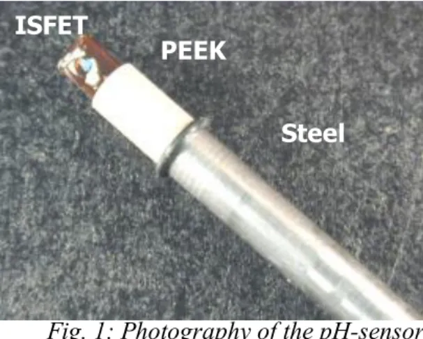
The 2 x 5 mm2 front side connected pH-ISFET chips were reported on the 5 x 8 mm2 tip.
After gold wedge wire bonding, they were encapsulated using polymer EP3HTMED (purchased from Master Bond, USP class VI requirements). This epoxy is biocompatible, possesses excellent resistance to chemicals and to different types of sterilization including gamma irradiation [4]. The mounted disposable sensor was implemented in a 8 mm diameter tube composed of PEEK (PolyEtherEtherKetones) and steel (Fig.1).
Fig. 1: Photography of the pH-sensor
Three ReMOS and three ISFET structures have been irradiated (Cobalt-60 ) according to the European standard EN552 with a dose of 25kGy [5].
ISFET
PEEK
Electrical characterization of the ISFETs was carried out by using a micro-reference electrode in teflon (World Precision Instruments). Transfer curves were extracted using a HP4041B analyser by monitoring the drain-source current in different pH values under constant drain-source voltage Vds =1 V. The sensitivity of the ISFETs, i.e the gate-source voltage
variation, was estimated under the following conditions: constant drain-source current (Ids =
100µA) and constant drain-source voltage (Vds =1 V).
3. Results and discussion
The behaviour of the three pH-ISFET microsensors has been tested in various pH buffer-solutions (pH: 4, 7, 10). In the same time the transfer curves for the three ReMOS were extracted. The quasi-nernstian sensitivity with good linearity was evidenced for the pH-ISFETs before irradiation. Then, the six structures were exposed unbiased at room temperature to gamma-radiation. The transfer curves Ids – Vgs of the ISFETs and ReMOS before and after
irradiation are shown in figures 2 and 3. The threshold voltage Vth of the ReMOS increases by
450 mV after gamma irradiation. That corresponds to the creation of a net effective negative charge of -2*10-8 C/cm2.
As shown in figure 3, the threshold voltage Vth of the ISFET sensors decreases by 220 mV. It is
due to an effective positive charge creation of +9.6*10-9 C/cm2. It should be noticed that these
shifts are of opposite sign contrary to what was expected since the gate insulators are the same in both structures.
0,0 0,5 1,0 1,5 2,0 2,5 3,0 3,5 4,0 0,0 0,2 0,4 0,6 0,8 1,0 1,2 1,4 1,6 1,8 2,0 before radiation after radiation I ds , m A Vgs, V V ds= 1V gate: Au/Ti/Si 3N4/SiO2 ReMOS
Fig. 2: Transfer curves of three ReMOS before and after a 25KGy γ-irradiation.
0,0 0,5 1,0 1,5 2,0 2,5 3,0 0,0 0,1 0,2 0,3 0,4 before radiation after radiation I ds , m A Vgs, V V ds= 1V gate: Si3N4/SiO2 Micro-electrode pH=4 ISFET
Fig. 3: Transfer curves of the ISFETs before and after a 25KGy γ-irradiation
The behaviour of the ISFET and ReMOS structures was analysed more deeply using X-ray irradiation. Structures were exposed during different durations (5 min, 10 min,30 min, 50 min, 180 min) with a radiation dose rate D = 350rad/min. The experiment was done by using a CGR Acquivolt 350 X-ray generator available in the laboratory. In this experiment, a
MOS dosimeter was used to measure the absorbed dose [6]. The experimental curves of ReMOS and ISFET structures are presented in figure 4.
1,0 1,1 1,2 1,3 1,4 1,5 1,6 1,7 1,8 1,9 2,0 0 200 400 600 800 1000 1,4 1,5 1,6 1,7 1,8 1,9 2,0 ISFET MO S thre s h o ld v o lt a g e , V ISF E T thre s h o ld v o lt a g e , V Dose, Gy pH=4 Vds =1V I ds =100µA REMOS
Fig.4 : ReMOS and ISFET threshold variations for different received doses
This experiment confirms that the shifts of the ReMOS and ISFET threshold voltages under irradiation are in the opposite direction regardless of the absorbed dose, and that the ReMOS is more sensitive than the ISFET.
In order to explain the negative charge generation and to see whether it was due to the insulator charge or to the interface states charge we have separated the contribution of the two kinds of charges using the midgap technique [7]. The doping level Na in the transistor channel
was evaluated from the slope S of the linear part of the curve Vth versus the substrate voltage
Vbs (see Figure 6).
The value was estimated to be 2.8*1015cm-3. The transconductance calculated from the slope of
the linear part of the curve in Fig 2 was 0.633 mA/V only slightly modified by the irradiation. Following calculation in [8] the current at midgap was Img = 44 pA.
0,0 0,5 1,0 1,5 2,0 2,5 3,0 3,5 4,0 4,5 5,0 1 2 3 4 5 d e lt a V t, V Vbs1/2 , V1/2 Vds=0,1V
Fig.5: The threshold voltage shift versus bulk-source bias
The subthreshold current of the ReMOS before and after irradiation is shown on Fig. 6. From this figure and the value of Img the midgap voltage shift ΔVmg due to irradiation was equal
to 0.21V corresponding to a generated insulator charge ΔQins = - 9.6 nC/cm2. Then considering
the threshold voltage shift ΔVth = 0.45V (see Fig 2) leads to a generated interface states charge
ΔQss=-10.6 nC/cm2. So it appears that contrary to what is generally expected in MOS devices
the charge in the bulk insulator created by the γ-irradiation is negative.
This may be explained by the presence of the nitride/oxide interface N/O which has been shown to trap either electrons or holes depending upon the direction and the magnitude of the electric field inside the insulator double layer [9]. In the present case a detailed analysis of the potential distribution in the structure considered without any charge at the N/O interface before irradiation and with an effective positive charge of 10 nCb/cm2 at the oxide/silicon interface as
evaluated from Vth before irradiation shows that the electric field in the nitride layer is negative
thus driving the electrons generated in the nitride layer towards the N/O interface where they can be trapped. This charge compensates or over compensates the positive charge in the oxide layer and adds to the negative charge of the interface states making the net effective charge negative. This analysis is similar to that developed to explain the compensation of radiation
effects in MNOS structures in [10] with the difference that in our case the field distribution in the insulating layers is not determined by the applied bias but by the built-in potential.
-3 -2 -1 0 1 2 3 4 5 1E-11 1E-10 1E-9 1E-8 1E-7 1E-6 1E-5 1E-4 1E-3 0,01 before radiation V th=1.25V after radiation Vth=1.7V I ds , A Vgs, V V ds= 1V
gate: Au/Ti/Si3N4/SiO2
ReMOS Ith I th_gamma I mg
Fig.6: Sub-threshold current curves for ReMOS un-irradiated and irradiated to 25kGy.
In the case of the ISFET the parallel analysis could not be performed because although the extrapolation of the subthreshold curve to the midgap situation shows a negative shift following irradiation the extrapolation was uncertain due to a large excess current in this region. However because during irradiation there is no electrode on top of the nitride layer the electric field in this layer is certainly very small if not zero. Consequently the electron-hole pairs generated in the nitride layer will disappear by initial recombination so that the positive charge trapped near the oxide/silicon interface will contribute alone.
2 4 6 8 10 1,8 1,9 2,0 2,1 2,2 2,3 2,4 2,5 2,6 2,7 2,8 2,9 3,0 V gs , V pH before radiation after radiation Ids=0,1 mA Vds=1 V ISFET
Fig.7: ISFET sensitivity before and after radiation
The response of the ISFET structure to the pH was also investigated before and after irradiation. Fig 7 shows the sensitivity curves obtained. It appears that the response is quite unchanged by the irradiation. A shift of the working point is only evidenced.
4. Conclusion
SiO2/Si3N4 front-side connected ISFET and ReMOS chips have been fabricated and packaged
in tubes in a way adapted to a bio-application use. The influence of γ-irradiation up to the standard sterilization dose was investigated. It has been shown that following irradiation the threshold voltage values of the two structures suffer a shift as usually but positively in the case of the ISFET and negative for the ReMOS. This behaviour has been explained by electron trapping at the nitride/oxide interface in the ISFET due to the trapping properties of this interface and the internal electric field distribution. Furthermore the slope of the transfer curves was not significantly modified.
The response to the pH of the ISFET was not modified by the irradiation so that γ-sterilization of pH-ISFETs appears as a viable solution. However, additional parameters must be investigated after irradiation such that reproducibility and stability of the response. Work is in progress in this sense.
Acknowledgements
This work was supported by the French company Fogale Nanotech.
References
[1] S. F. D'Souza, Biosensors for fermentation process control Microbial biosensors Biosensors and Bioelectronics, Vol.16, 2001, p 337-353
[2] S. Herrmann, W. Oelßner, H. Kaden, M. Brischwein and B. Wolf The influence of different methods of disinfection on the function of electrochemical sensors, Sensors and Actuators B69, 2000, p 164-170
[3] P Temple-Boyer, J. Launay, I. Humenyuk, T. Do Conto, A. Martinez, C. Bériet, A. Grisel, Study of front-side connected chemical field effect transistors for water analysis, Microelectronics Reliability, 44 (2003), 443-447.
[4] W. Oelßner, J. Zosel, U. Guth, T. Pechstein, W. Babel, J. G. Connery, C. Demuth, M. Grote Gansey and J. B. Verburg, Encapsulation of ISFET sensor chips, Sensors and Actuators B 105, 2005, p 104-117
[5] Byron J. Lambert and Joyce M. Hansen, ISO radiation sterilization standards, Radiation Physics and Chemistry, Vol. 52, 1998, p. 11-14
[6] G. Sarrabayrouse and V. Polischuk, MOS ionizing radiation dosimeters: from low to high dose measurement, Radiation Physics and Chemistry, Vol. 61, 2001, p 511-513 [7] P.S. Winokur, J. R. Schwank, P.J. McWhorter, P.V. Dressendorfer, D.C. Turpin,
Correlating the radiation response of MOS capacitors and transistors, Nuclear Science, IEEE Transactions on, Vol. NS-31 1984 p:1453 – 1460
[8] S.M. Sze, Physics of semiconductor devices, 1981 (New York: John Wiley&Sons), p.446
[9] Takahashi, Y.; Ohnishi, K.; Fujimaki, T.; Yoshikawa, M, Radiation-induced trapped charge in metal-nitride-oxide-semiconductor structure, Nuclear Science, IEEE Transactions on, Vol. 46, 1999 P: 1578 – 1585
[10] J.R. Cricchi and D.F. Barbe, Compensation of radiation effects by charge transport in metal-nitride-oxide-semiconductor structures, Applied physics letters, Vol. 19, 1971, p. 49 - 51