HAL Id: hal-03092725
https://hal.archives-ouvertes.fr/hal-03092725
Submitted on 4 Jan 2021
HAL is a multi-disciplinary open access
archive for the deposit and dissemination of
sci-entific research documents, whether they are
pub-lished or not. The documents may come from
teaching and research institutions in France or
abroad, or from public or private research centers.
L’archive ouverte pluridisciplinaire HAL, est
destinée au dépôt et à la diffusion de documents
scientifiques de niveau recherche, publiés ou non,
émanant des établissements d’enseignement et de
recherche français ou étrangers, des laboratoires
publics ou privés.
Optimization of deep rib high speed phase modulators
on 300mm industrial Si-photonics platform
Stephane Monfray, Sébastien Cremer, Nathalie Vulliet, Emmanuel Dubois,
Florian Domengie, Sebastien Jan, Francoise Baille, Frederic Boeuf
To cite this version:
Stephane Monfray, Sébastien Cremer, Nathalie Vulliet, Emmanuel Dubois, Florian Domengie, et al..
Optimization of deep rib high speed phase modulators on 300mm industrial Si-photonics platform.
SPIE Photonics Europe, Conference 11364 - Applications of Photonic Technology - Integrated
Pho-tonics Platforms: Fundamental Research, Manufacturing and Applications, Apr 2020, Strasbourg,
France. 1136403, 8 p., �10.1117/12.2554725�. �hal-03092725�
Optimization of Deep Rib High Speed Phase Modulators
on 300mm Industrial Si-Photonics Platform
S.MONFRAY
1, S.CREMER
1, N.VUILLET
1, E.DUBOIS
2, F.DOMENGIE
1, S.JAN
1, F.BAILLE
1, F.BŒUF
11 STMicroelectronics, 850 Rue Jean Monnet, Crolles, 38920, France,
2IEMN, Cité Scientifique, Avenue Poincaré, BP 60069, 59652 Villeneuve d'Ascq, France
stephane.monfray@st.com
Abstract— This paper highlights the optimization of Deep Rib
High Speed Phase Modulators for 400G applications thanks to the optimal choice of structure and implants through a Design Of Experiment analysis, including the proposal of a new Deep Rib HSPM with Z-implants. Results show 1,6dB gain in OMA (Optical Modulation of Amplitude) at the same cutoff frequency (fc=[2Pi*RC]-1) compared to the previous generation [1] with
optimized vertical implants, and up to 2,15dB gain vs [1] with the new Z-implant Deep Rib device.
Keywords—photonics, Deep Rib PN junction modulators
I. INTRODUCTION
Silicon photonics technology provides unreached data densities and integration level while taking benefits from low cost and industrial manufacturing infrastructure of CMOS electronics [1]. In this paper, O-band Silicon PN junction modulators have been designed and integrated. In order to improve light confinement in the core for maximizing the modal overlap with PN junction, we optimized a Deep Rib architecture. The purpose of this paper is to demonstrate the optimization of the modulator to obtain the best optical performances and speed with optimized implants and structure thanks to a DOE (Design Of Experiments) analysis, and to propose a new combination of well implants (named Z-implants) with the optimized Deep Rib geometry to reach OMA (Optical Modulation Amplitude) value as high as -2dBm with high cut-off frequency.
II. DOE DEVICES INTEGRATION ON 300MM PHOTONICS
PLATFORM
A Design Of Experiments (DOE) for Deep Rib modulators was tested on our 300mm Si-Photonics platform, including Ge Photodiodes, Si & SiN waveguides and transitions (see Fig.1) for CWDM circuits.
The Design of Experiments (DOE) for Deep Rib modulators was first established with variations on the junction position Xj
(from 20nm to 160nm), on the width of the modulator (W from 320 nm to 600nm) and on the distance d of access arms implants to the guide (from 100nm to 400nm) with different levels of doping (Process of reference Arm Doping x1 and highly doped Arm Doping x20), see figures 2a and 2b.
Fig.2a: Parameters used in the DOE definition. We studied the width (W) impact, the junction (Xj) position and the Arm implants Dose and position (d = d_Arm).
Fig.2b: Fabricated HSPM devices with Deep Rib structure. Total guide thickness=300nm and Arm thickness=50nm are constant parameters for the DOE.
To extract the intrinsic cut-off frequency (fc) of the modulator PN junction, a so-called OPEN deembedding procedure has been applied to eliminate RC parasitics associated to the probing pads and interconnect layers from the topmost Metal4 to the inner Metal2 layers. This involves two distinct S-parameters measurements of the active device and of the passive OPEN structure, respectively. By subtracting the admittance of the OPEN from that of the modulator PN junction, the intrinsic RC product is subsequently easily determined to yield fc. All RF
measurements were performed with a reverse PN junction bias of 1.8V. The figure 3 shows that by reducing the distance to the waveguide of the Arm implants combined with a high dose (x20 vs industrial reference [1], R can be largely reduced leading to high fc.
Fig 3 shows the measured cutoff frequency in function of d distance, for two levels of Arm Doping (x1 and x20) vs previous industrial reference [1])
However, this optimization has to take into account the impact on optical performances (in particular losses) induced by the
Fig.1: 300mm Si Photonic Platform including Si & SiN waveguides, adiabatic transition, Thick M4 Cu level and Deep Rib HSPM modulators. Integrated Ge PD is not shown on the picture.
doping modification. To explore this, we decided to monitor the OMA (Optical Modulation Amplitude) value for all structures of the DOE. OMA is defined as the difference between the optical power levels (Phigh and Plow) of the signal. The value of OMA is calculated based on the extracted HSPM parameters: α=total device Losses (dB/mm), PS=device Phase Shift (°/mm) and L=device length (mm).
𝑂𝑀𝐴 (𝑑𝐵𝑚) = 10. 𝐿𝑜𝑔10(𝑃ℎ𝑖𝑔ℎ − 𝑃𝑙𝑜𝑤) 𝑃ℎ𝑖𝑔ℎ = 10^ (−∝.𝐿 10 ) . 𝑐𝑜𝑠²( 𝜋 4− 𝑃𝑆.𝐿 180. 𝜋 2) 𝑃𝑙𝑜𝑤 = 10^ (−∝.𝐿 10) . 𝑐𝑜𝑠²( 𝜋 4+ 𝑃𝑆.𝐿 180. 𝜋 2)
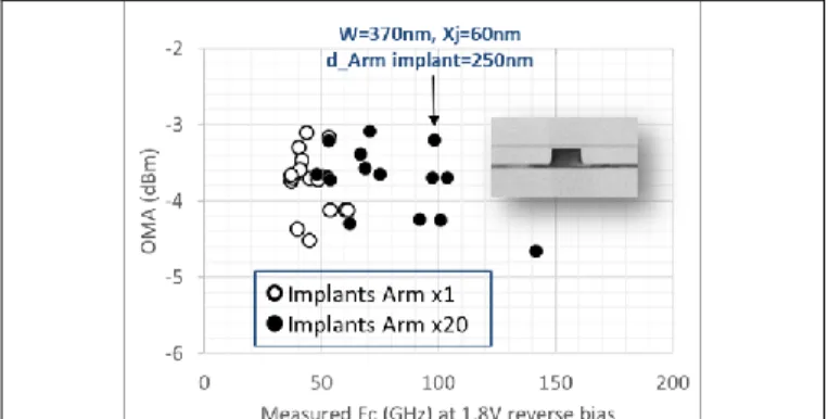
We highlighted that by increasing by a factor 20 (N=1e19cm-3)
the implant dose in the access arms down a distance to the waveguide d=250nm, the cutoff frequency could be highly improved (fig.3) without penalty on optical performances (fig. 4). For shorter distance, higher losses lead to OMA decrease.
Fig 4: impact of the Arm implant distance from the Si guide on the optical performances (OMA), for two levels of Arm doping (reference and x20).
III. OPTIMIZED DEVICES INTEGRATION WITH VERTICAL PN
IMPLANTS
In order to determine the best structure, we first performed TCAD simulations of all DOE structures to evaluate the access resistance, while other parameters (capacitances, losses, phase-shift) where measured on the fabricated devices.
Thanks to the DOE analysis, we determined that the best optical performances was obtained for Xj=60nm and a width of 400nm. Experimentally, the closest measured device had a width of 370nm and was highlighted as the best point of our OMA vs fc (=1/2PiRC) figure of merit (fig.5).
Fig 5: DOE results for different geometrical and implants parameters. Best structure for compromise OMA vs cut-off frequency is identified. L=2,4mm.
The same DOE was then measured with the RF structures (fig. 6) to extract the exact fc with a reverse bias of 1,8V, and confirmed the best performances for our identified experimental geometry (W=370nm, Xj=60nm, d_Arm implant distance=250nm) with the highest Arm implant dose (x20 vs the previous platform).
Fig 6: Confirmation of best geometry confirmed with cut-off frequencies measured at 1,8V reverse bias on dedicated RF structures. L=2,4mm.
Then we optimized the value of the Waveguide (Wells) implants by increasing sequentially the dose of Pwell and Nwell vs the reference. The figure 7 show that we improved OMA by increasing both values by a 1,5 factor.
Fig.7: (left) Impact of Si guide Pwell implant increase for a given Nwell value and (right) Impact of Si guide Nwell implant increase for the best Nwell implant. OMA is optimum for the highest values. L=2,4mm.
Finally, compared to our previous industrial platform (Rib modulators in [1]) we can see on figure 8 that the optimized Deep Rib structure improves the OMA by 1,6dB with an improved cut off frequency (1/2PiRC).
Fig 8: Impact of well implants increase for the best HSPM geometry. OMA is improved from -3,25dBm to -2,85dBm on the Deep Rib structure. L=2,4mm. Compared to [1], OMA is improved by 1,6dB.
The figure 9 provides OMA vs L characteristic for the best device.
Fig 9: OMA vs L for the Optimized geometry and optimized implants (Arm x20) & (Nwell x1,5) & (Pwell x1,5) vs ref implants [1].
IV. NEW DEEP RIB DEVICES INTEGRATION WITH Z IMPLANTS
We propose in this section the combination of our best Deep-Rib geometry with Z-implants (combination of depths of vertical N-well implants ) to improve the coverage between the highly confined mode in the Deep-Rib structure and the depletion zone of the PN junction (fig.10).
Fig 10: Proposal of new Z-implant structure on Deep-Rib best architecture. Z-implants are optimized to ensure a better electrostatic coverage of the optical mode (left) vs the classical vertical implants (right).
The same DOE was analyzed with these Z-implants and the best geometry was the same as previously identified, but with Xj=140nm to ensure the best overlap with the junction. Fig.11 & 12 shows the optical performances of the structure and compare it with the previous points. One can see that this approach improves OMA by 2,15dB compared to our previous platform, by assuming a slight decrease of the cut-off frequency.
Fig 11: Optical performances of the new HSPM Deep Rib with Z-implants measured on the best design (W=370nm, d_Arm=250nm, Xj=140nm)
Fig 12: Performances of the best HSPM geometry with the new Z implants on Deep Rib structure (Arm implants x20, d_Arm=250nm, W=370nm, Xj=140nm). Compared to [1], OMA is improved by 2,15dB. L=2,4mm.
The figure 13 provides OMA vs L characteristic for the best device.
Fig 13: OMA vs L for the optimized geometry, optimized implants (Arm x20) & Z-implants on Deep Rib structure.
Finally, we compared the 3 structures: Rib modulator from [1], the optimized vertical PN Deep-Rib modulator (from fig.8) and the Deep-Rib modulator with Z-implants. OMA (calculated based on experimental data) in function of device length graphs and VPi*LPi highlight the improvement proposed by those
structures compared to the reference platform.
Fig 14: OMA vs L for the Optimized Deep Rib geometry and optimized implants (Arm x20) & Z-implants compared to the previous industrial platform [1].
Fig 15: VPi*LPi for the Optimized Deep Rib geometry and optimized implants (Arm x20) & Z-implants compared to the previous industrial platform [1].
V. CONCLUSION
This paper shows optimized deep Rib modulators for 400G and above applications. DOE integration allowed us to define the optimal structure and implants to guaranty high speed (high cutoff frequency) coupled with high optical performances, to propose highly performant silicon PN junction modulator with OMA improved by 1,6dB and up to 2,15dB compared to the industrial state-of-the-art. The best Deep Rib geometry with Z-implants has OMA (Optical Modulation Amplitude) value as high as -2dBm (L=3mm) with 54GHz@0V cut-off frequency. This work was partially supported by H2020 project N° 688516 COSMICC and project IRT Nanoelec.
[1] F.Boeuf et al., “Silicon Photonics R&D and Manufacturing
on 300-mm Wafer Platform” JOURNAL OF LIGHTWAVE TECHNOLOGY, VOL. 34, NO. 2, JANUARY 15, 2016
![Fig 3 shows the measured cutoff frequency in function of d distance, for two levels of Arm Doping (x1 and x20) vs previous industrial reference [1]) However, this optimization has to take into account the impact on optical performances (in particular](https://thumb-eu.123doks.com/thumbv2/123doknet/14436675.516144/2.918.473.852.351.567/measured-frequency-function-industrial-reference-optimization-performances-particular.webp)