HAL Id: hal-01834195
https://hal.archives-ouvertes.fr/hal-01834195
Submitted on 10 Jul 2018
HAL is a multi-disciplinary open access
archive for the deposit and dissemination of
sci-entific research documents, whether they are
pub-lished or not. The documents may come from
teaching and research institutions in France or
L’archive ouverte pluridisciplinaire HAL, est
destinée au dépôt et à la diffusion de documents
scientifiques de niveau recherche, publiés ou non,
émanant des établissements d’enseignement et de
recherche français ou étrangers, des laboratoires
Magnetoresistive Random Access Memory
Dmytro Apalkov, Bernard Dieny, J. Slaughter
To cite this version:
Dmytro Apalkov, Bernard Dieny, J. Slaughter. Magnetoresistive Random Access Memory.
Pro-ceedings of the IEEE, Institute of Electrical and Electronics Engineers, 2016, 104, pp.1796 - 1830.
�10.1109/JPROC.2016.2590142�. �hal-01834195�
Magnetoresistive Random Access Memory
Dmytro Apalkov
1, Bernard Dieny
2, J. M. Slaughter
31. Samsung Electronics, Semiconductor R&D Center, San Jose, California, USA. 2. SPINTEC, Grenoble Alpes Univ, CEA, CNRS, CEA/Grenoble, INAC, Grenoble, FRANCE 3. Everspin Technologies, Inc., Chandler, Arizona, USA
Abstract
A review of the developments in MRAM technology over the past 20 years is presented. The various MRAM generations are described with a particular focus on Spin-Transfer-Torque MRAM (STT-MRAM) which is currently receiving the greatest attention. The working principles of these various MRAM generations, the status of their developments, and demonstrations of working circuits, including already commercialized MRAM products, are discussed.
Keywords: MRAM, spintronics, spin electronics, magnetic tunnel junctions, tunnel magnetoresistance, spin transfer torque, STT-MRAM, toggle, thermally assisted MRAM
OUTLINE
1. Introduction to MRAM technology
1.1 Magnetic tunnel junction devices for MRAM 1.2 Overview of MRAM technology generations
2. Major advancements that enabled MRAM and stimulated commercial development
2.1 Tunneling Magnetoresistance
2.2 Synthetic antiferromagnet (SAF) structures and their application to MRAM 2.3 Savtchenko Switching
2.4 Spin-Torque Switching
2.5 Interfacial perpendicular magnetic anisotropy
3. Demonstrations of working MRAM circuits 4. Requirements for reliable read in an array 5. Field-written toggle MRAM
5.1 Operating principles of toggle MRAM 5.2 Performance of toggle MRAM 5.3 Applications of toggle MRAM
6. Spin-Transfer-Torque-MRAM (STT-MRAM)
6.1. Introduction
6.2. Fundamentals of STT-MRAM 6.2.1. STT-MRAM trilemma
6.2.1.1. Information recording: STT writing 6.2.1.2. Information storing
6.2.1.3. Simultaneous achievement of writability, readability and retention 6.2.2. Breaking STT-MRAM trilemma
6.2.2.2. Device design improvements
6.2.2.2a. In-plane STT-MRAM with PPMA
6.2.2.2b. Perpendicular MTJ design (p-STT-MRAM) 6.2.2.2c. MTJ structure with two MgO barriers: DMTJ 6.3. STT-MRAM: Remaining challenges
6.3.1. Patterning process
6.3.2. Switching probability: write and read error rates 6.3.3. Read disturb
6.3.4. Long-term data retention 6.3.5. MTJ endurance and breakdown 6.4. STT-MRAM Chip demonstrations
6.5. STT-MRAM: Conclusion and outlook
7. Thermally Assisted-MRAM (TA-MRAM)
7.1. Dilemma between retention and writability / benefit from thermally-assisted writing 7.2. Heating in MTJ due to tunneling current
7.3. In-plane TA-MRAM
7.3.1. Write selectivity achieved by a combination of heating and field 7.3.2. Reduced power consumption thanks to low write field and field sharing 7.4. TA-MRAM with soft reference: Magnetic logic unit (MLU)
7.5. TA-MRAM with soft reference: Multilevel storage 7.6 Thermally assisted STT-MRAM
7.7 Remaining challenges and conclusion regarding Thermally Assisted MRAM
1. Introduction to MRAM technology
Magnetoresistive random access memory (MRAM) is a class of solid-state storage circuits that store data as stable magnetic states of magnetoresistive devices, and read data by measuring the resistance of the devices to determine their magnetic states. In practice, the magnetoresistive devices are integrated with CMOS circuitry to make chips that are compatible with mass-produced semiconductor electronics. Such circuits have been designed around a variety of magnetoresistive devices, but commercially-produced MRAM products, and the vast majority of MRAM technologies being developed for future commercial MRAM technologies, are based on magnetic tunnel junction (MTJ) devices. All of these circuits are resistive memories in terms of the read operation; it is the method of writing the magnetic state that sets apart the different types of MRAM technology. Some of the heavily-studied write methods include Stoner-Wolfarth-type field switching, Savtchenko switching (also a field-switching method), spin-torque switching, and thermally-assisted switching (heat with field or spin torque). Two methods have so far been commercialized: toggle MRAM, which uses Savtchenko switching[1], has been in mass production since 2006,[2] and spin-torque switched MRAM is in the early-stages commercial production[3].
Advances in MRAM technology have been closely linked with advances in the understanding of magnetic and magneto-transport properties of ultra-thin films, including: tunneling magnetoresistance (TMR), MgO-based MTJ materials for giant TMR, synthetic antiferromagnet (SAF) structures, interfacial perpendicular magnetic anisotropy (PMA), and spin-transfer torque (STT). The application of scientific discovery to commercial technology seen in this field is striking in its breadth and speed of adoption. In this paper we review the major developments that are driving accelerating interest and adoption of MRAM, key considerations for functionality and scaling to higher densities, and the status of the major technology types.
1.1
Magnetic Tunnel Junction Devices for MRAM
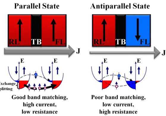
Figure 1 shows the most basic magnetic tunnel junction structure, two ferromagnetic layers separated by a dielectric spacer layer, the tunnel barrier. When the tunnel barrier is very thin, typically < 2nm, quantum mechanical tunneling of electrons through the barrier makes the MTJ behave like a resistor having a resistance that depends exponentially on the barrier thickness and is proportional to the inverse of the in-plane barrier area. The tunneling current is spin-polarized, due to the asymmetric band structure of the ferromagnetic electrodes, giving rise to the tunneling magnetoresistance as shown in Figure 1. The relative orientation of the magnetizations in these two layers determines the resistance of the MTJ device. For most materials, the resistance is low when the magnetizations of the two layers are parallel, because the majority band electrons can tunnel into the majority band on the opposite side of the barrier. When the orientation is antiparallel, the resistance is high since the majority band electrons have to tunnel into the minority band of the opposite electrode.
Figure 1. Sketch of a magnetic tunnel junction: two ferromagnetic layers (in red/blue) typically made of CoFe based alloys separated by a tunnel barrier (black) most often made of MgO about 1nm thick. Explanation of the tunneling magnetoresistance effect: parallel state has good band matching and low resistance, whereas antiparallel state has poor band matching: either absence of available carriers of a given spin or inadequacy of available states in the receiving electrode.
The simplest possible STT-MRAM design has the following components: - Free layer (FL)
- Tunnel Barrier (TB) - Reference layer (RL)
The free layer, sometimes called recording layer or storage layer, is the ferromagnetic layer retaining the stored information. This layer is often made of CoFeB material of different compositions[4]. The tunnel barrier is a thin (around 1 nm) insulating non-magnetic layer, that provides means to switch and read the state of the free layer with a spin-polarized tunneling current. In the past ten years, MgO tunneling barriers have been most heavily studied due to the giant TMR effect, though other materials, such as AlOx, and TiO have been used [5] and AlOx is used in production toggle MRAM. The other magnetic layer – the reference layer – provides a stable reference magnetization direction for the FL reading and switching. This layer is designed to have magnetic anisotropy much higher than the FL so that it never switches during memory operation.
Although multi-bit concepts exist, the MTJ devices that have been demonstrated in practical MRAM circuits have two stable magnetic states that store one bit of data as a parallel/antiparallel magnetic state with a low/high resistance as described above. To achieve this, such a magnetic device has a free layer engineered to have a uniaxial
magnetic anisotropy, so that the magnetization tends to lie along an easy axis in one or the other direction. Since the magnetization of ordinary ferromagnetic thin films is constrained to be in the film plane by the thin-film shape anisotropy, the in-plane easy axis is created mainly by patterning the free layer into a shape with a long direction (easy axis) and short direction (hard axis). The intrinsic anisotropy of the material may also contribute to the total uniaxial anisotropy. On the other hand, devices having their easy axis perpendicular to the film plane can have a number of advantages, discussed further in the sections that follow. A free layer engineered to have a perpendicular easy axis has stable states with the magnetization either up or down, with respect to a horizontal film plane, and the in-plane directions are hard. Such layers employ materials having a strong perpendicular anisotropy that can overcome the thin-film shape anisotropy, also discussed below. For any of these devices, the stability of the stored data over time and temperature is determined by the energy barrier between the two stable magnetic states, which is in turn related to the strength of the uniaxial anisotropy and the volume of magnetic material involved in the reversal process.
To create a memory array from MTJ devices, each device is typically integrated with an isolation transistor that can be turned on to pass a current selectively through the MTJ devices of interest, such as during the read operation. For spin-torque MRAM, the same transistor is used to pass the switching current through the target MTJ devices. Since each memory cell typically has one transistor and one MTJ, this particular architecture is known as the 1T-1MTJ MRAM architecture. Other architectures have been proposed and evaluated for various purposes, but the 1T-1MTJ cell is the most commonly used.
Fig.2: Sketch of the organization of field-written MRAM. Each cell comprises an MTJ connected in series with a select transistor.
1.2
Overview of MRAM technology generations
MRAM technology can be classified by the switching method employed to write data. First-generation MRAM is generally understood to include methods using magnetic fields to program the array. Toggle MRAM is the only first-generation MRAM in mass production [2], [6], [7]. A strong advantage of field switching is unlimited write endurance, since reversing the free-layer magnetization with a magnetic field does not create any wear-out effects. A disadvantage is the difficulty in scaling to smaller cell sizes, due to several factors including the magnitude of the
required switching currents and the somewhat complex memory cell geometry. A detailed discussion of this technology is presented in the section on Field-Switched MRAM.
Second-generation MRAM uses spin-transfer torque (STT) to program the array. STT switching can be accomplished with reasonable efficiency with MTJ devices having either in-plane or perpendicular-to-the-plane magnetization. STT-MRAM with in-plane devices began commercial production in 2015 with a 64Mb product [3] and is expected to ramp to volume production in 2016 with a 256Mb product[8]. STT-MRAM with perpendicular MTJ devices is under intensive development at a number of companies around the world. A discussion of technology demonstration vehicles, the fundamentals of the technology, and relative advantages/disadvantages is presented in several sections below.
A number of physical phenomena are under investigation for use in third generation MRAM, including: voltage-controlled anisotropy (VCA), voltage-controlled magnetism (VCM)[9]–[12], spin Hall effect (SHE) and spin-orbit torque switching (SOT)[13]–[17]. The potential for improved MRAM scaling and performance comes from idea that switching could be accomplished while passing little or no electrical current through the MTJ device. However, each effect has challenges to overcome for use in practical MRAM circuits. Some examples of those challenges are as follows. VCA does not directly lead to deterministic switching between two stable states, but is more likely to be applied in combination with another innovation for use in an MRAM array. Reliability issues like wear-out and parameter drift need to be better understood for practical VCM devices. SHE does not lend itself to efficient switching in devices with perpendicular magnetization, and SOT appears to require innovation in materials to increase the magnitude of the effect for improved switching efficiency. In many cases, these new devices would need to be deployed in a three-terminal cell configuration that is not compatible with high-density memory arrays. Nonetheless, the possibility of switching with little or no charge current passing through the tunnel barrier is stimulating a growing interest and investment due to the potential for use in low-power circuits and high-endurance applications.
2. Major advancements that enabled MRAM and stimulated commercial development
2.1 Tunneling Magnetoresistance
The development of magnetic tunnel junction (MTJ) material with high room-temperature magnetoresistance ratio, MR~10%, reported in 1995 [18], [19] offered a much improved read signal for MRAM technology. This major development in tunneling magnetoresistance (TMR) was followed by intensive work around the world that resulted in dramatic improvements in the techniques and materials, so that record TMR values have increased steadily, most markedly with the development of MgO tunnel barriers [4], [20], [21] to over 600%[22]. In addition to having a high magnetoresistance, MTJ materials also provide the ability to match the resistance of the storage device to that of the CMOS transistors used in the circuitry. This capability is essential to the technology since the transistors used in the MRAM read circuit result in a series resistance, typically in the kΩ range, that reduces the relative resistance change at the point of sensing. The giant magnetoresistance (GMR) and anisotropic magnetoresistance (AMR) devices, that
were available prior to practical MTJ devices, are inherently low resistance since they are metallic and therefore not well suited to integration with CMOS circuitry.
The promise of practical, high-TMR, materials motivated new MRAM R&D programs around the world, leading to the first commercial product [23], [2] approximately 11 years after the initial discovery [18],[19]. These materials also had a large positive impact on the hard disk drive (HDD) industry where MTJs were quickly commercialized for improved read sensors. Although the detailed requirements for MTJ devices in read sensors are quite different from the MRAM case, there is no doubt that the huge development effort in MTJ materials for HDD readers greatly accelerated the progress in MTJ materials for MRAM.
2.2 Synthetic antiferromagnet (SAF) structures and their application to MRAM
The discovery and intense study of oscillatory magnetic coupling (RKKY-coupling) in synthetic layered structures, in the 1980s, showed that it was possible to engineer thin film structures with separate ferromagnetic layers that are coupled either ferromagnetically or antiferromagnetically to each other through a nonmagnetic spacer layer separating them, with a coupling strength and sign determined by the thickness of the spacer [25]. This understanding led to the use of synthetic antiferromagnet (SAF) structures engineered to provide the required magnetic properties for both reference magnetic layers and free layers in MTJ devices for MRAM. Almost all MTJ devices for MRAM use a SAF for the reference layer. A SAF reference layer has strong antiferromagnetic (AF) coupling between ferromagnetic (FM) layers of nearly equal magnetic moment, resulting in a magnetically rigid system. When used as a free layer, the spacer layer thickness is set for weaker AF coupling to make a less rigid structure that is more responsive to applied magnetic fields as described further in sections that follow.
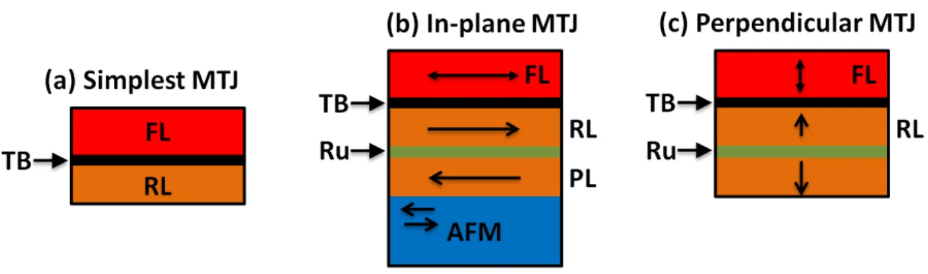
The simplest design of an MTJ is represented in Fig.3a. It exhibits tunnel magnetoresistance. However it has undesired magnetostatic interactions between the RL and the FL, which tend to bias the FL toward the antiparallel (AP) state (for in-plane magnetization).
Figure 3. (a) Simplest MTJ design. (b): Typical in-plane MTJ with a synthetic antiferromagnetic reference layer pinned by an antiferromagnetic (AFM) pinning layer; (c) perpendicular MTJ with synthetic antiferromagnetic reference layer.
A typical in-plane MTJ with a SAF reference structure is illustrated in 3b. In this example, the pinned layer of the SAF (PL) is pinned in a specific direction by direct contact with an underlying antiferromagnetic (AFM) material, and the reference layer of the SAF (RL) is in contact with the tunnel barrier providing the reference direction for the MTJ. The SAF performs two major functions: it provides a stable magnetic reference direction since its low net moment is less affected by external fields than a single ferromagnetic layer, and the imbalance of magnetic moment between the two layers can be easily adjusted to provide a negative dipolar field that cancels the positive interlayer coupling between the reference layer and the free layer [26]. The interlayer coupling can include Neel coupling, due to magnetic poles created by correlated roughness at the surfaces of the layers, [27] and an electron-mediated coupling associated with the polarized electrons tunneling through the barrier, both of which favor ferromagnetic alignment of the reference and free layers. A typical MTJ with perpendicularly magnetized SAF and free layer is shown in 3c. The same principles apply in this geometry although, due to the extremely high anisotropies achievable with engineered perpendicular materials, the pinning AFM layer is not necessary.
A SAF structure for the free layer serves a different purpose and has very different design requirements compared to a SAF reference structure. The main use of a SAF free layer is to enable the Savtchenko switching technique used in toggle MRAM, which is described further in the section below.
2.3 Savtchenko Switching
Writing data into a memory array requires the ability to select the storage devices to be written within a large array of such devices, switch those target devices with extremely high reliability, and leave all other devices unaffected with extremely high reliability. For field-switched MRAM, this proved to be a significant challenge [26]. The basic idea of field switching is to use rows and columns of write lines, placed under and over the MTJ devices, that create magnetic fields large enough to reverse the free layer magnetization for the devices located at the cross point where both a row and column line are energized (See Fig.2). The fundamental problem with this approach is that all of the non-target bits along the energized lines also see a field that, although smaller in magnitude, causes a non-negligible probability of switching those half-selected bits. This is known as the “half-select problem.”
The half-select problem for field switching was solved with the invention of Savtchenko switching, [1] which cleverly employs a SAF free layer and a sequence of write-current pulses that creates a rotating field to switch it. MRAM that uses Savtchenko switching is usually called “toggle MRAM” because the switching technique toggles the SAF free layer from one stable state to the other using the same write pulse sequence, as opposed to using different fields to write the high or low state. The first commercially-produced MRAM product was a 4Mb toggle MRAM which began production in 2006 by Freescale Semiconductor. That part and a family of products based on the same technology platform, now produced by Everspin Technologies, account for nearly all of MRAM production and sales today, with the remainder being Everspin’s 64Mb STT-MRAM product.
The spin-transfer torque effect was theoretically predicted independently by J. Slonczewski and L. Berger in 1996 [28], [29]. When a current is passed between two ferromagnetic layers separated by a non-magnetic spacer, it exerts a torque on the magnetization of each of the layers. If the current is high enough, this can result in switching of the free layer. The first demonstration of STT induced magnetization switching was done by Katine et al. using a spin valve device made from all-metal GMR stack in 2000 [30]. The first STT switching demonstration with MTJ devices was by Huai, et al. [5] in 2004 on AlOx-based tunneling junctions and 2005 on MgO-based MTJ [31]–[33].
2.5 Interfacial perpendicular magnetic anisotropy
Magnetic materials can exhibit magnetic anisotropy large enough to overcome the thin-film demagnetization energy and to pull the magnetization of the film out-of-plane. Many scientific studies in the late 1980s and early 1990s laid the foundations for rapid application of such materials in data storage and later in MRAM development. Perpendicular magnetization has been demonstrated in multilayered ultra-thin films and superlattices having a ferromagnetic material layered with a nonmagnetic material, such as Au, Pt, or Pd [34], [35], [36], and for similar structures made from two different ferromagnetic materials, Co and Ni [37]. This perpendicular anisotropy can have several origins associated with spin-orbit interactions: electronic hybridization effects, interfacial strain, magnetocrystalline anisotropy etc. A comprehensive survey of experimental studies on these materials can be found in reference [38].
In perpendicular MTJs, both the storage layer and reference layer are magnetized out-of plane (Fig.3c). For the reference layer, synthetic antiferromagnetic multilayers have become the preferred materials due to their strong and tunable perpendicular anisotropy energy and compatibility with fabrication techniques normally used for MTJ materials. As discussed above, practical use requires a SAF reference structure in MTJ devices for MRAM. Such SAF materials have been successfully and extensively developed and integrated into MgO-based pMTJ materials[39]– [41].
In addition to the SAF reference structure, pMTJ materials for MRAM also require a perpendicular free layer with soft magnetic properties that enable efficient spin-torque switching between the two stable states (up and down). Of particular importance for STT-MRAM was the discovery that a quite strong perpendicular anisotropy exists at the interface between magnetic metal and oxides such as (Co/AlOx or CoFe(B)/MgO) [42], [43]. This anisotropy has been shown to result from hybridization effects between the transition metal (Co,Fe) dz² orbitals and the oxygen orbitals of the oxide tunnel barrier [44], [45]. In STT-MRAM, this strong interfacial anisotropy provides a good thermal stability of the free layer magnetization together with a sufficiently low write current as explained in section 6.
Development of CoFeB-based free layers with first one MgO interface, [43] and later two MgO interfaces, [46], [47], combined with the multilayer-based perpendicular SAF materials, has led to practical pMTJ devices with the desired low switching current and high energy barrier needed for nonvolatile memory. STT-MRAM circuits and technology based on such pMTJ devices are in advanced development at a number of companies worldwide.
3. Demonstrations of working MRAM circuits
The major advancements described in the previous section have been successfully incorporated into a number of MRAM demonstration circuits and commercial products. Some notable demonstrations of working circuits are described below, illustrating the rapid progress in technology development over the past 15 years.
In 2000, Scheuerlein, et al. reported the functionality of a field-switched MRAM circuit using AlOx-based MTJ devices and Stoner-Wolfarth-type writing circuits [48]. Basic read and write functionality were demonstrated in a 1 kb memory array with write pulses as short as 2.5ns and with read operation as short as 10ns, using a twin-cell read configuration.
Durlam, et al. described the first Toggle MRAM circuit in 2003, a fully-functional 4Mb circuit with 1T1MTJ architecture and AlOx-based MTJ devices, demonstrating the effectiveness of Savtchenko writing to solve the problem of high write error rates due to the half-select in Stoner-Wolfarth-type field switching[49]. This circuit was designed to be a product, not simply a demonstration, with a unique local-bitline array architecture, a cell size of 1.55 µm2, asynchronous 16-bit SRAM interface compatibility, and demonstrated symmetric read and write cycle times of less than 25ns [6]. This chip was introduced as a commercial product in 2006 and continues to be produced today by Everspin Technologies, Inc.
Significant results from several ST-MRAM demonstration circuits, all using MgO-based MTJ devices, have been published, beginning with a 4kb test vehicle in 2005 [50] followed by many others including: a 2Mb circuit and device data in 2007 [51], statistical data on 4 kb integrated arrays with 70×210 nm2 bits [52] and devices with perpendicular magnetization [53] in 2008, arrays integrated with 54nm CMOS technology [54], 4kb MRAM arrays with perpendicular bit switching in 2010 [55].
The first ST-MRAM product, announced in 2012, is a 64Mb, DDR3, ST-MRAM circuit [56], [3]. Shown in Figure 4, the chip is fabricated using in-plane MTJ devices in a 1T1-MTJ cell, integrated with 90nm CMOS technology and packaged in a JEDEC standard DDR3 BGA. This chip is compatible with available DDR3 memory controllers and became commercially available from Everspin Technologies, Inc. in 2015.
Figure 4. Everspin 64Mb DDR3 ST-MRAM Die Photo. Word line drivers run vertically through the center of each of eight 8Mb banks. Strips of column circuits run horizontally, dividing each bank into 8 sub-arrays.
In 2014 Thomas, et al. reported performance data for an 8Mb STT-MRAM demonstration chip with high energy barrier for data retention compatible with automotive applications and MTJ devices that are tolerant to high processing temperatures required for embedded memories [57]. Although CMOS circuitry is 90 nm technology, MTJ devices with diameter as small as 45nm were used, demonstrating reliable switching with pulses as short as 2ns in a 1T1MTJ cell architecture.
The continuous improvement reported in these papers, and many others, reflects significant innovation and progress toward the use of spin-torque switching in a wider range of products, including stand-alone memories and embedded memory in a multiple applications.
4. Requirements for reliable read in an array
The MTJ device should have a resistance in the kΩ range to minimize the effect of the series resistance from the isolation transistor. This resistance typically leads to a tunnel barrier thickness on the order of 1 nm. The exponential thickness dependence of RA creates a challenge for producing MTJ material that is repeatable and uniform over the area of wafers used in semiconductor production. The issues of cross-wafer uniformity and wafer-to-wafer repeatability have largely been solved by the manufacturers of MTJ productions tools that are capable of <1% uniformity and repeatability for these ultra-thin films. However, array uniformity, which is a measurement of bit-to-bit resistance variation within a memory array, is a continuing challenge as device sizes are scaled ever smaller.
During the read operation, a typical read circuit compares the resistance of the bit to a reference resistance in order to determine if the bit is in the high or low state. Figure 5 illustrates the effect of random resistance variations within an array on this type of read circuit. In the low state, bits with resistance on the high side of the distribution will fall closer to the reference than the average bit. Conversely, the bits on the low side of the distribution in the high resistance state will also be closer to the reference. To have working memories with bit counts of Mb or more, the circuit must be able to correctly read the state of these bits in the tails of the distributions. If bits that are statistically separated 5σ from the mean are unreadable, there will be approximately one bad bit in 2Mb, a marginally unacceptable result requiring error correction.
Figure 5. Schematic representation of Gaussian resistance distributions for a large array of MTJ cells in the low- and high-resistance states. A midpoint reference, represented here by Rref, is generated by the read circuitry to evaluate the state of the MTJ device by comparing the measured resistance to Rref. The average change in resistance from the low to high state is ∆R, but the circuit must be capable of determining the resistance change for cells in the tails of the distributions, meaning the resistance change available to the circuit is ∆Ruse.
A reasonable criterion for feasibility is 6σ separation from the midpoint, or 12σ separation between the mean high and low resistance states. Since the circuit must be able to correctly read the low 6σ bits in the Rhigh distribution, and the high 6σ bits in the Rlow distribution, the useable resistance change for the circuit ∆Ruse is the difference between the midpoint reference and the 6σ tails as illustrated in Figure 5. A larger ∆Ruse allows a more aggressive circuit design with faster access time. It will make the read-out more robust, less sensitive to noise, and can be used for higher speed operation. To account for high-speed reading with normal process variations in the circuitry, significantly more than 12σ is required. For example, Toggle MRAM in production has demonstrated over 20σ separation [49].
A number of factors can contribute to the width of the resistance distribution. Any variation in the bit area, e.g. due to lithography or etch variations, will directly cause variations in bit resistance. Process damage or veils created during the etch process also may contribute. However, it has been shown that the quality of the MTJ tunnel barrier itself can make a significant contribution to bit-to-bit resistance variation [23]. As the size (area) of MTJ devices is reduced, a given variation in the MTJ dimensions from the patterning process will create a larger relative bit-to-bit variation in the resistance. In addition, a given level of inhomogeneity in the tunnel barrier will result in a
similar increasing relative variation with decreasing device size. As a result, maintaining a given level of separation in the resistance distributions for a robust mid-point read operation requires improvements in both the patterning process and the quality of the tunnel barrier.
For cases when separation between the high and low resistance distributions is not sufficient for reading with a mid-point reference scheme in a 1T-1MTJ architecture, other methods and/or cell architectures can be employed. A twin-cell architecture, has two MTJ devices, in a 2T-2MTJ memory cell or in two adjacent 1MTJ cells, that are always written in opposite states to effectively double the resistance change. A circuit employing this cell was used to demonstrate high-speed MRAM read in one of the first MRAM demonstration circuits [48]. The trade-off for the higher read performance is array area; twice as much area is needed for a given memory density.
Another method for mitigating the effect of wider distributions is the self-referenced read [58]–[62]. There are different techniques for self-referencing, but they all involve comparing the resistance of the MTJ in its initial state (stored data) to its resistance after being switched or rotated to a known state. For example, the resistance can be measured and stored, then compared to its resistance after a known switching pulse. Since the resistance of a device is compared to the same device in a different state, the bit-to-bit resistance distribution no longer plays a primary role. In another approach, based on big differences in resistance dependence on voltage in parallel and antiparallel states, two measurements are done at different voltage values and results are compared[63]. In all the self-referenced read schemes, the trade-off for the tolerance to wide resistance distributions is longer time for the read operation, due to the extra pulse and the second read access time.
5. Field-written toggle MRAM
A memory array for field-written MRAM typically has rows and columns of copper lines above and below the MTJ devices that generate magnetic fields when current pulses are passed through the lines (See Fig.2). Three key innovations that enable the successful commercialization of field-written MRAM are: Savtchenko switching for Toggle MRAM operation, improvements in tunnel barrier quality and bit patterning fidelity for narrow and well-behaved bit-to-bit MTJ resistance distributions, and the process for cladding of the write lines. As described briefly in section 2.3 and in more detail in the section on Toggle MRAM below, Savtchenko switching solved the half-select problem through the use of a SAF free layer and timed write pulses. Another method of addressing the half-select problem, by using a combination of magnetic field and heat for thermal-assisted switching, is described in section 7. The importance of narrow read distributions is described in the preceding section and is important to all types of MRAM circuits.
Cladding involves the addition of permeable ferromagnetic material around three sides of a write line to focus the magnetic field toward the fourth side [64]. This produces a stronger field at the MTJ devices located near the fourth side, above or below the line, and minimizes the stray fields in other directions. The effect is to significantly
reduce currents needed for the write operationand to suppress possible write errors due to stray fields experienced by rows or columns of bits adjacent to the row or column of bits to be written.
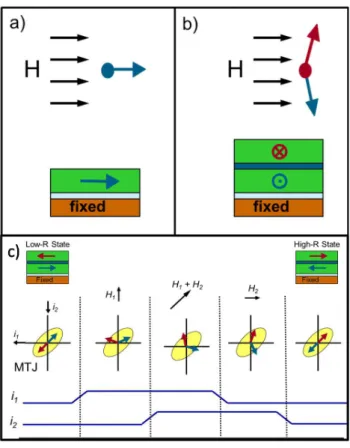
5.1. Operating principle of Toggle MRAM
The use of Savtchenko switching in MRAM arrays provides a number of benefits including: low write error rates, reduced sensitivity to external fields, and a wide operating region for the write currents that reduces sensitivity to manufacturing process variations [7]. It relies on the unique behavior of a synthetic antiferromagnet (SAF) free layer, formed from two nearly identical ferromagnetic layers separated by a non-magnetic coupling spacer layer. As shown schematically in Figures 6a and b, a single free layer responds to an external field by aligning with it, while the behavior of a SAF free layer is quite different. For a SAF having some net anisotropy Hk in each layer, there exists
a critical spin flop field Hsw at which the two antiparallel layer magnetizations will rotate (flop) to be approximately
orthogonal to the applied field H, with each layer scissoring slightly in the direction of H [65]. For fields H ≥ Hsw, the
SAF can lower its total energy by decreasing its dipole energy with a flop and scissor, even though the antiferromagnetic exchange energy is increased by the same scissoring. As the applied field strength is increased, the layers of the SAF will scissor further until they eventually become parallel and aligned with the field at the saturation field Hsat.
Figure 6. (a) A single layer of ferromagnetic material responds to an external field (H) by aligning with it, while the behavior of a SAF is quite different. A SAF free layer (b) rotates such that the moments of the layers are nearly orthogonal to H when the magnitude of H reaches the flop field of the SAF, with the moments canting to produce a net moment approximately
parallel to the field. As the field strength is increased, the moments scissor toward each other until they are parallel when the SAF is saturated. (c) Schematic of a toggle MRAM bit with the field sequence used to switch the free layer from one state to the other. The fields, H1, H1 + H2, and H2 are produced by passing currents, i1 and i2, through the write lines.
The programming pulse sequence and resulting response of the free layer are shown in Figure 6c. To toggle the bit from an initial ‘0’ to a final ‘1’ the currents i1 and i2 are pulsed with the timing indicated in the figure, such that
the vector sum of the two magnetic fields effectively rotates through 90°. The SAF responds by orienting nominally orthogonal to this field and rotating with it such that, when i2 is turned off, the moments relax to their easy-axis the
magnetization of each layer now reversed. Because the TMR only depends on the direction of the layer that is in contact with the tunnel barrier, the resistance switches states each time the toggle pulse sequence is applied.
The toggle write mode requires that the memory circuit first determine the state of the target bit, and execute the toggle pulse sequence only if it is not in the desired state, i.e. only if the new data differs from the existing. If the pre-read determines that the target bit is already in the desired state for the new data, then that bit is not toggled. This approach increases the total write cycle time by adding a read operation, but has benefits in limiting the overall power consumption and improves array efficiency because the unipolar current allows the use of smaller transistors in the write drivers.
The elimination of the half-select problem can be understood by considering the energy barrier to reversal of bits experiencing a field from a single line (½-selected bits). For a SAF free layer, the single-line field raises the energy barrier of those bits, so that they are stabilized against reversal during the field pulse. This is in marked contrast to the conventional approach using a simple ferromagnetic layer for storage, where all of the ½-selected bits have their switching energy reduced and are therefore more susceptible to disturbance (thermal or external field).
5.2. Performance of Toggle MRAM
A major feature of Toggle MRAM is the essentially unlimited write endurance, since there is no wear-out mechanism related to switching the magnetization state of the free layer with magnetic fields. During the read operation, the bias applied to the MTJ is at a level far below the breakdown voltage of the device, but finite bias leads to a finite probability of eventual dielectric breakdown. For product reliability, two MTJ barrier failure modes must be controlled: time dependent dielectric breakdown (TDDB) and resistance drift. Dielectric breakdown is an abrupt drop in resistance, or shorting, of the tunnel barrier, while resistance drift is a gradual reduction of the junction resistance over time that can eventually lead to increased read error rates.
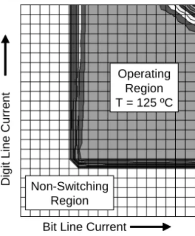
Many applications in industrial and automotive applications, require consistent performance and robust reliability over a broad operating temperature range, typically -40 °C < T < 125 °C. Rigorous reliability analysis done for the Everspin 4Mb MRAM product showed that it exceeds the reliability requirements of industrial and automotive products[66]–[68]. Extensive operational characterization and accelerated stress testing validated its full functionality and high reliability in this environments. Figure 7 demonstrates that the Toggle switching operating region is maintained at the highest temperatures with more than ample margin.
Figure 7 Toggle switching map at elevated temperature (T= 125 ºC) showing large operating region. Saturation of the free layer SAF exchange can start to be observed at over driven currents at the upper right in the figure. (From Ref. [68])
In the operating region, it is possible to reliably read data and write to the array within the 35ns read/write cycle time for this part. The large region with no switching errors is a demonstration of the ability of Savtchenko switching to eliminate half-select disturbs, even when the elevated temperature (125C) causes some reduction of the SAF coupling strength.
Everspin’s commercial Toggle MRAM uses an MTJ device with AlOx tunnel barrier and NiFe SAF free layer. The SRAM-like parts are specified for full cycle time of 35ns for both read and write, but selected parts have been demonstrated to operate to <25ns. Improved read speed has been demonstrated by replacing AlOx with an MgO-based MTJ [24]. Although the relative resistance distributions with MgO are wider than for AlOx, with sigma~1.5% as compared to sigma~0.9% for AlOx, the higher MR provides more separation between the high and low resistance distributions, resulting in more usable signal for the read circuit. The MRAM cells using MgO and the NiFe SAF had double the MR compared to AlOx-NiFe, and 42% larger MR/σ, resulting in a reduction of the read cycle time from 21 ns to a circuit-limited 17 ns. Much faster read times are possible for circuits optimized to take advantage of the higher read signal.
5.3 Applications of Toggle MRAM
Toggle MRAM parts are used in a variety of different markets including: data storage, transportation, networking, and industrial automation. The combination of nonvolatility, unlimited endurance, high random access performance, and a wide operating temperature range, provides specific market advantages in many of these applications. Often the MRAM chip is replacing another type of memory as well as a battery or capacitor, providing a significant reliability benefit. The main factor limiting further market penetration is the limited memory density, with 16 Mb being the highest density in production. The next higher density MRAM chip currently in production is the 64 Mb part using STT switching [3]. Toggle MRAM is also used as an embedded memory in system-on-chip (SoC) applications. Embedded memories are often much smaller density than stand-alone memories, making Toggle
Operating Region T = 125 ºC
Non-Switching Region
Bit Line Current
D ig it L in e C u rr e n t Operating Region T = 125 ºC Non-Switching Region
Bit Line Current
D ig it L in e C u rr e n t
MRAM competitive with incumbent technologies. Since the MTJ layer is inserted between metal layers in the back-end part of the process, fabricating embedded MRAM is no different than fabricating standalone memory.
The application that consumes the largest number of MRAM chips today is RAID data storage systems. MRAM chips with densities usually in the 1Mb to 4Mb range are used in these systems to store metadata, such as restart vectors, controller parameters, system configuration data, and various tables. In case of power failure, this system information is inherently saved in the nonvolatile memory and can be accessed quickly upon restart. This application requires fast, unlimited reads and writes, combined with nonvolatility and high reliability. In this and similar applications, a Toggle MRAM part with a parallel interface often replaces some type of SRAM combined with a battery or capacitor to enable data retention when power is lost, providing higher reliability and a lower cost solution.
In transportation and industrial applications, the wide operating temperature range and impressive data retention time are important factors. Toggle MRAM arrays, based on 180 nm technology, have demonstrated data retention times over 20 years at 125 C, as well as reliable operation from -40 C to 125 C [68]. Since MTJ devices store data with a magnetic state, rather than charge, they have advantages over charge-based memories for space and military applications where exposure to ionizing radiation is an issue. The same MRAM arrays used for industrial grade MRAM are integrated with special radiation-hard CMOS to address those markets.
The higher densities enabled by STT switching is enabling MRAM technology to move into additional storage applications, including caching and buffering, as well as other sockets typically filled by a DRAM.
6. Spin transfer torque MRAM (STT-MRAM)
6.1. Introduction
One of the limitations of field-switched MRAM introduced at the beginning of this review is the difficulty of maintaining low error rates and high data retention while reducing the size of the MTJ devices. The first effect of shrinking the device dimension is an increase in the switching field distribution width, affecting write currents and error rates, and further shrinking results in loss of data retention time. Although toggle MRAM at the 180nm or 130nm technology nodes has a very large thermal stability factor ∆, maintaining a sufficiently large ∆ for smaller free-layer volume would eventually require a larger anisotropy field HK that is difficult to achieve with shape anisotropy. These
two scaling issues have led industry to shift from toggle switching to STT switching for technology nodes of 90nm and below.
To understand the fundamental physics behind the spin transfer torque effect, we can use the free-electron model. Let us consider a structure consisting of two ferromagnetic layers separated by a non-magnetic spacer layer (Fig. 8). When a current goes through one ferromagnetic layer, the electrons become spin-polarized along the magnetization of this layer due to spin-dependent scattering, as shown in Figure. 8. As the spin-polarized current enters the other ferromagnetic layer, the spin of transmitted electrons precess incoherently around the local exchange field which is along the magnetization of this layer. This exchange field results from the exchange interactions between the spin of the conduction electrons and those responsible for the local magnetization. As a result of that, within a very short distance of the order of 1 nm, the electron current becomes repolarized along the magnetization of the second ferromagnetic layer. Due to momentum conservation, the difference between the momentum of the incoming and outgoing electron currents yields a torque acting on the magnetization of the second ferromagnet – this torque is known as spin-transfer torque [28], [29]. Several materials can be used to separate the two ferromagnetic layers. When this material is conducting, the corresponding trilayer structure (ferromagnet-conductor-ferromagnet) is called a spin-valve (SV)[69]. Alternatively, if the material is insulating the resultant structure becomes a magnetic tunneling junction (MTJ).
Figure 8. Free-electron model for spin transfer torque. The electrons get spin-polarized in the first ferromagnetic layer (polarizer or RL – reference layer) with spin aligned parallel to magnetization of the polarizer MRL. As the electrons transverse the free layer (FL), their spin is repolarized towards the magnetization of the FL. Due to the momentum conservation, the difference of the incoming and outgoing spin-polarized current gives rise to STT torque.
Magnetoresistance and spin-transfer torque can be viewed as closely-related effects. In magnetoresistance, the magnetic structure (parallel or antiparallel orientation of magnetizations) affects the electrical properties of the stack, notably resistance (see Fig. 1). In STT effect, it is the electric current being passed through magnetic structure that can change its magnetic state. In both cases, the fundamental origin lies in the exchange interactions between the spin of conduction electrons (determining electrical properties) and the localized spins (responsible for the magnetic properties).
6.2.
Fundamentals of STT-MRAM
The application of spin-transfer torque writing in MRAM allowed a large reduction of switching current as compared to field-switched MRAM (Fig. 9). As the bit becomes smaller, the writing current decreases proportionally to the MTJ area down to a minimum value dependent on the cell thermal stability factor and other parameters characteristic of the material used for the storage layer.
Figure 9. Structure of conventional field-switched MRAM cell as compared to STT-MRAM cell.
In addition to that, STT-MRAM has a simpler geometry (Fig. 9), eliminating landing pad, word and bypass lines that allows scaling down to cell size of 4-6F2, where F is the semiconductor feature size. For reducing the cell size even further, it is possible to introduce multiple MTJ elements in one STT-MRAM cell [70]. Such MLC (Multiple-Level Cell) designs will pose more challenges to reduce the writing/reading margins and will likely reduce speed of operation.
(b) STT-RAM Cell (a) Conventional MRAM cell
Si substrate Gate MTJ Bit line 6 F2 Source Drain Landing Pad Si substrate Gate MTJ Bypass Line Bit line
Write Word Line
Cladding
20-30 F2
6.2.1 STT-MRAM trilemma
Any memory including STT-MRAM has to provide the following basic functionalities: writing the data, retaining the written data for a predefined period of time (retention) and reading the recorded information. This section describes challenges of achieving these three properties together.
6.2.1.1 Information recording: STT writing
In order to discuss details of the STT-MRAM operation, it is necessary to introduce how the spin-transfer torque results in switching. The magnetization dynamics of any magnetic layer can be described by the Landau-Lifshitz-Gilbert (LLG) equation [71]:
(
)
;
;
0 0m
H
Γ
m
m
H
Γ
Γ
Γ
m
×
×
−
=
×
−
=
+
=
αγµ
γµ
damp prec damp precdt
d
, (1)where
m
≡
M
M
S is the normalized vector along the magnetization M of the magnetic layer with saturation magnetizationM
S, H is the total effective magnetic field (including anisotropy and applied fields), α is Gilbert damping, γ the gyromagnetic ratio and µ0 the vacuum permeability. The first termΓ
prec in (1) describes theprecessional motion of magnetization around the effective field H while the second term
Γ
damp describes the gradual damping of the magnetization precessional motion towards the effective magnetic field H, hence reducing its total energy.When spin-transfer torque acts on a magnetic layer such as the storage layer in STT-MRAM, two additional terms appear in the LLG equation[28]:
With
(
)
RL S P STT RL S IP STT STT P STT IP damp prect
M
e
J
t
M
e
J
dt
d
m
m
Γ
m
m
m
Γ
Γ
Γ
Γ
Γ
m
×
=
×
×
=
+
+
+
=
1
2
;
1
2
' 0 0h
h
η
γµ
η
γµ
(2)where J is the current density, t is the thickness of the free layer, e - the electron charge,
h
is the Planck constant, η is the spin transfer efficiency (directly related to the current spin-polarization).Γ
IPSTT is the torque lying in the plane defined by the two vectorsm
andm
RL and hence often called in-plane torque, or damping-like torque (since it has the same form as the Gilbert damping but can change sign depending on the current direction and therefore can behave as an antidamping torque) or Slonczewski torque. The second torqueΓ
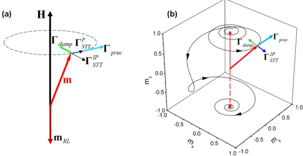
PSTT lies perpendicular to this plane and hence is often called perpendicular spin torque or field-like torque. Concerning the magnetization dynamics induced by STT, in the most relevant case of axial symmetry whenm
RL||
H
, the perpendicular STT has the sameeffect as the precessional torque term i.e. its main effect is to change the frequency of the magnetization precession. In contrast, the plane STT can either enhance or reduce the damping torque, as depicted in Fig. 10. When the in-plane STT opposes the damping torque and overcomes it in magnitude, the amplitude of the precession increases to a point where magnetization switching can occur as illustrated in Fig. 10b. The current at which this happens is commonly referred to as critical switching current Jc0.
This action of in-plane STT is often described as a “negative damping” or an “anti-damping” [72], [73]. For switching consideration, usually the in-plane torque is most important. However the perpendicular torque can become relevant in certain specific problems [74]. An example of the switching trajectory for the case of spin torque overcoming damping torque is shown in Fig.10b. The initial orientation of the magnetization is along +Z axis. The notable change in precession chirality as mz crosses zero (counterclockwise to clockwise looking downwards on XY
plane) is a signature of spin torque switching and is due to the change of sign of the anisotropy field between upper and lower hemispheres (pointing along +Z for mz>0 and –Z for mz < 0).
Figure 10. Spin-transfer torques acting on the magnetization (a) and resulting switching trajectory (b).
By solving the LLG equation, the following expressions for the critical switching current of in-plane (IP) and perpendicular to plane (PP) magnetized storage layer (respectively case of Figure 3b and 3c) were derived [75]:
( )
( )( )
s K PP c K eff s IP cH
t
M
e
J
H
H
t
M
e
J
h
h
0 0 0 02
1
2
2
1
µ
α
η
µ
α
η
=
+
=
⊥ (3)where
η
is the spin transfer efficiency, and α, t,H
K,H
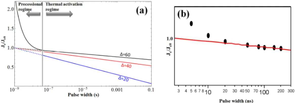
⊥eff are respectively the magnetic damping constant, thickness, in-plane anisotropy field and out-of-plane demagnetizing field of the FL, respectively. At this value of the current, effective damping is equal to zero and any infinitesimal precession of magnetization becomes unstable. However, the switching time strongly depends on the actual value of the current density with respect to the value of Jc0. As a rule of thumb, if the measurements are done at T=300 K, Jc0 is close to the average switching currentdensity for pulse width tp~10-20 ns. For longer pulse width, the average switching current density reduces due to thermal fluctuations, which help the magnetization to overcome the energy barrier. Two regimes in Jc(tp) are
commonly observed, as shown in Figure 11:
- For very short pulses (tp<10ns), the switching current density is larger than Jc0 and during switching, details
of individual magnetization precession are important – this is commonly referred as “precessional or ballistic regime”. In this precessional regime at T = 0K, switching current for a given pulse width
t
p is given by the following expression [76]:,
2
ln
1
0 0
+
=
θ
π
τ
p PP c PP ct
J
J
(4)where
τ
=
(
αγµ
0H
K)
−1 is the characteristic relaxation time,θ
0 is the initial angle between the magnetization and the easy axis when the current pulse is turned on.From expression (3), it is clearly seen that for a given damping, spin torque efficiency and memory retention (the latter being directly related to Hk), STT-MRAM with perpendicular anisotropy should operate with lower switching current density. This and other reasons described below explain why most of the R&D in STT-MRAM is focused on cells based on out-of-plane magnetized MTJs. If the switching is performed at non-zero temperature, there will be two important effects due to random thermal fluctuations. First, the initial angle
θ
0 will be distributed according to Maxwell-Boltzmann distribution [73], introducing distribution of switching current for a given pulse width. This effect is most important for short pulse width, typically for tp<20-50 ns –see Figure.11. Second, thermal fluctuations will affect the switching process itself.-For longer pulse width values, usually for tp>50-100 ns – this switching regime is called thermally-activated regime (Fig.11). In this case, STT effect starts to play a secondary role by increasing effective temperature of the magnetization, thus increasing thermal fluctuations, which in turn, help the magnetization to overcome the energy barrier. The boundary between the two regimes is not very well defined and depends on the FL properties but usually this boundary corresponds to switching current near but less than
J
c0. Based on thermal activation model, the following expression has been derived for STT-MRAM in thermally-activated regime:[76]–[78]
=
∆
−
=
FL
PP
for
2
FL
IP
for
1
,
ln
1
1
1 0 0τ
ξ
ξ pw c ct
J
J
(5)where ∆ is the thermal stability factor (ratio of energy barrier for switching in stand-by Eb=µ0MsHkV/2
divided by the thermal activation kBT, V being the volume, kB the Boltzmann constant, T the temperature),
τ
0 is anintrinsic attempt time of the order of 1ns and the parameter
ξ
is equal to 1 or 2 for respectively in-plane and out-of-plane magnetized FL [78], [79], [77]. This dependence is often used to experimentally determine Jc0 and ∆ for IP FLby measuring median Jc at different pulse width spanning a few decades, and fitting Jc as a function of log(tp) and
extrapolating to 1 ns: the slope yields the thermal stability ∆ and the extrapolated Jc (1 ns) gives Jc0. This approach
(with
ξ
=
1
) has also been used for PP FL. However it was shown to give inaccurate results unless fitting withξ
=
2
is used [78].Figure 11. Dependence of switching current density on current pulse width: precessional and thermally activated regimes by modeling (a) and typical experiment (b). Behavior of the STT-MRAM cells with equal Jc0 but different thermal stability factor ∆is shown in thermally activated regime (a). The data correspond to in-plane magnetized FL. Perpendicular FL exhibit qualitatively similar behavior.
6.2.1.2. Information storing
Similar to field-switched MRAM discussed earlier in this review, the information retention capability is determined by the energy barrier Eb that the free layer magnetization has to overcome to switch to opposite state in
stand-by divided by the thermal activation energy at the operation temperature [80]:
T
k
E
B b=
∆
(6)This expression holds for both in-plane and perpendicular STT-MRAM free layer. For small dimensions and high density, perpendicular STT-MRAM is preferred, as will be discussed later.
Typically, ∆ > 60-80 is needed to guarantee reliable data retention for 10 years. For IP free layer, the energy barrier is provided by shape anisotropy (thus requiring elongated shapes) and is given by the following expression:
T
k
V
M
H
T
k
E
B S K B b IP2
0µ
=
=
∆
(7)For in-plane free layer with elliptical cross section with short axis of dimension w, one can derive a simplified expression for the effective anisotropy field:
(
)
wAR
AR
t
M
H
KIP S1
2
−
=
(8)Where AR is the in-plane aspect ratio: length divided by width. Thus, the thermal stability becomes:
( )
(
)
T
k
AR
w
t
M
B S IP8
1
2 0−
=
∆
µ
π
(9)From this expression, we can see that the stability of in-plane magnetized cells is proportional to the square of the moment per unit surface (Mst) and width of the cell. Mst is a quantity that can easily be measured by VSM
magnetometry. This expression, which is derived based on assumption that the free layer magnetization switches uniformly (macrospin approximation) is in good agreement with experimental observations, provided that AR is not excessively large (<2.5-3) and macrospin approximation is valid.
For FL with perpendicular magnetization, a general expression for the anisotropy energy density can be written as follows:
2
2
1
2 0 0 S PP K S i PP b PPH
M
M
t
K
K
=
+
σ
−
µ
=
µ
, (10)where
σ
i is the perpendicular surface anisotropy per unit surface taking into account the two interfaces of the FL, PPb
K
is the bulk anisotropy (per unit volume). The term -1/2 µ0Ms² is the demagnetizing energy which tends to bring back the magnetization in-plane.Two classes of PMA materials are often distinguished based on the dominant origin of anisotropy [81]: - B-PMA (bulk perpendicular magnetic anisotropy)
- I-PMA (interfacial perpendicular magnetic anisotropy)
The former usually involves materials, which have crystalline anisotropy due to reduced crystalline symmetry, making in-plane and out-of-plane directions inequivalent. Examples of such materials are FePt and CoPt alloys or multilayers. In most of these materials, binary or ternary alloys are used and at least one constituent material has high atomic (Z) number, which provides high spin-orbit coupling and correlatively large damping. While strong
anisotropy is beneficial for perpendicular STT-MRAM free layer, large damping is not desired since switching current is proportional to damping (Equation 3).
The latter, I-PMA anisotropy is related to interaction between the ferromagnetic film and the adjacent layer. An important class of I-PMA materials are based on the interface between a metallic ferromagnet and an oxide, which was demonstrated in 2002 using Pt/CoFe/AlOx structures[44], [82], [83]. Since the presence of Pt is undesirable due to an increase in damping from the spin-pumping effect, the same I-PMA at magnetic metal/oxide interface was later demonstrated in Pt-free structures suitable for STT-MRAM, namely Ta/CoFeB/MgO structures [41], [43]. This material has several important advantages as compared to B-PMA materials: very good lattice matching with MgO, low damping combined with large interfacial anisotropy and high spin-polarization yielding a large TMR amplitude. However, one challenge when using I-PMA materials is to obtain a sufficiently high thermal stability, especially at small (sub-20nm) dimensions. In B-PMA material, increasing the FL thickness while keeping everything else the same provides an easy and effective way to increase the thermal stability of the FL:
T
k
t
D
M
K
B S PP b B PP QU4
2
2 2 0π
µ
−
=
∆
− , (11)where “B” stands for B-PMA, QU stands for quasi-uniform approximation (i.e. assuming that the magnetization of the FL switches uniformly) and D is the diameter of the free layer.
In contrast, for I-PMA, assuming that the interfacial anisotropy is a property of the interface and does not change as the thickness of the ferromagnetic layer increases, the thermal stability decreases with thickness according to:
T
k
D
T
k
D
t
M
B i B S i I PP QU4
4
2
2 2 2 0π
κ
π
µ
σ
=
−
=
∆
− , (12)where we have introduced i i 0
M
S2t
2
µ
σ
κ
=
−
as the perpendicular magnetic anisotropy per unit area. This parameter plays a very important role in PMA free layer. It directly determines how small a given free layer can be made while still being stable, as will be discussed later in the text., The expressions of ∆ in the two equations above were derived assuming coherent macrospin switching of the free layer, which works well at very small cell dimensions (typically below 30nm in diameter) For both I-PMA and B-PMA materials but has significant discrepancies with experimental data at larger dimensions (See Fig.12) [84]. Indeed, at large dimensions, the evolution of ∆ versus the cell dimension observed experimentally is different from the D² quadratic behavior predicted by eq. (11) and (12). Rather, it exhibits a saturation for D>40nm, as illustrated in Figure12 below.The two main approaches to increasing ∆ for I-PMA free layers include increasing
σ
i and reducingM
S. A useful approache for obtaining more interfacial anisotropy energy includes the use of two MgO interfaces, one oneach surface of the FL [46][85]. This enables the approximate doubling interfacial anisotropy acting on the FL magnetization.
Figure 12. Experimental dependence of thermal stability ∆ on the junction size (reprinted from [47] with permission). These data exhibit saturation of ∆ at larger diameters indicating nonuniform magnetization reversal.
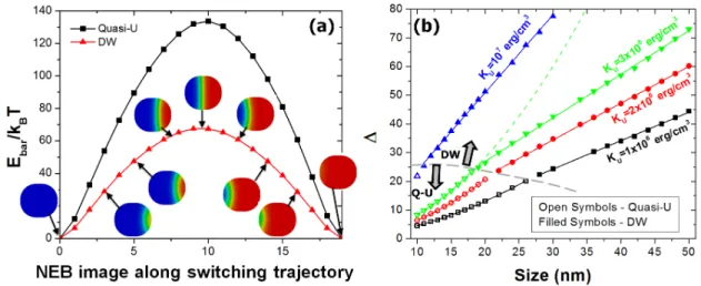
This change of behavior in the evolution of ∆ versus diameter between small and large dimensions is related to a change in switching mode from coherent rotation at small dimensions to nucleation/propagation reversal of magnetization at larger dimensions [86]. As a matter of fact, at dimensions above 40nm, much less energy is required to reverse the FL magnetization by nucleating a reversed domain in the FL and propagating a domain-wall across the FL than to switch the magnetization coherently. This can be demonstrated by a Nudged Elastic Band (NEB) simulation [87]. This method consists in constructing a series of magnetic states of the free layer connecting the initial and final states (e.g. magnetization “up” and magnetization “down”). Then, each image is moved along local energy gradient while keeping the images equidistant. This procedure is repeated until convergence is found. The resultant series of images corresponds to a switching path that has minimum energy barrier. This procedure was applied to a perpendicular FL with typical parameters and it was found that even for relatively small dimensions (20-30 nm), switching by a quasi-uniform rotation results in a much larger energy barrier than switching by domain-wall formation and propagation [46], [86] (see Fig.13). Thus, equations (11) and (12) must be replaced by the following approximate expression that describes the energy needed to create a domain wall across the diameter of the free layer:


![Figure 12. Experimental dependence of thermal stability ∆ on the junction size (reprinted from [47] with permission)](https://thumb-eu.123doks.com/thumbv2/123doknet/13386383.405064/28.892.315.625.228.523/figure-experimental-dependence-thermal-stability-junction-reprinted-permission.webp)