Université du Québec
Institut National de la Recherche Scientifique Centre Énergie, Matériaux et Télécommunications
Carbon Nanomaterials for Dye-Sensitized Solar Cells
byMahyar Mohammadnezhad
Dissertation submitted for the partial fulfillment of the requirements of the degree, Doctor of Philosophy, Ph.D.
in Energy and Materials Science
Evaluation Juries
Research supervisor Prof. Federico Rosei, INRS-EMT
Internal examiner and Prof. Fiorenzo Vetrone, INRS-EMT president of the Jury
External examiner Prof. Fabio Cicoira,
Polytechnique Montreal
External examiner Prof. Rafik Naccache,
Concordia University
ABSTRACT
According to the late Nobel Laureate Richard E. Smalley, energy is one of the biggest problems to be faced by humanity over the next 50 years. At the dawn of the 21st century, with the rapid development of industrialization and globalization, worldwide energy demands have rapidly increased. Different forms of fossil fuels represent over 80% of the world’s energy use. However, the limited availability of fossil fuels, together with climate change and environmental pollution dictates a transition towards sustainable, clean and carbon-neutral energy sources, including wind power, hydroelectric and solar energy. Amongst different sources of renewable energy, solar energy is one of the cleanest energy resources to be considered as a viable alternative to fossil fuels since sunlight is the most abundant of all available carbon-free energy sources. A solar cell is an optoelectronic device that directly converts the energy of light into electricity by the photovoltaic (PV) effect. Silicon (Si) solar cells currently constitute the most widespread commercial product in this field due to their high conversion efficiency and relatively long-term stability compared to other solar cell technologies. However, their high production cost and environmental impact are restricted to the terrestrial PV market. In recent years, dye-sensitized solar cells (DSSCs) have been regarded as a promising alternative to Si solar cells. DSSCs are considered as a promising future technology due to their appealing features, including a simple fabrication process, eco-friendly materials, colour choice and transparency. DSSCs must pass three main filters for large-scale commercialization: power conversion efficiency (PCE); long-term stability; and production cost. Although the design of new and modified devices that are structured to fabricate highly efficient cells are widely investigated, thus far the long-term stability and production costs have rarely been investigated and reported in the field of DSSCs.
The first part of this thesis demonstrates the effect of adding carbonaceous materials, in particular multi-wall carbon nanotubes (MWCNTs), on the stability of DSSCs under continuous simulated sunlight, indoor and ultraviolet (UV) light irradiation. After light aging, DSSCs are characterized by different techniques, to document the degradation mechanisms. The results indicate that MWCNTs can act as a strong conductive support and reinforcement of the titanium dioxide (TiO2) matrix, which is able to significantly
improve the long-term stability of DSSCs under continuous simulated one sun and indoor light by 22% and 42%, respectively. Based on UV stability measurements, MWCNTs, as an efficient absorbing and blocking agent for UV light, can successfully stabilize DSSCs for long-term operation with a 24% improvement in UV stability.
The second part of this work describes an investigation into the effect of incorporating MWCNTs in the thermal stability of DSSCs. Under identical measurement conditions (aging at 80°C for 240 h in the dark), standard DSSCs present a significant loss in PCE, dropping to 59% of their initial value, while a composited device with MWCNTs attained a promising thermal stability with only a 20% reduction. This loss in cell performance in standard DSSCs is mainly associated with a dramatic reduction in short circuit current density (Jsc). The composite anode exhibited excellent microstructure stability due to the bonding between MWCNTs and TiO2 nanoparticles. Furthermore, transient photovoltage decay and electrochemical impedance spectroscopy (EIS) measurements confirm the higher electron lifetime and reduction in charge recombination in the composite network due to the excellent conductivity of MWCNTs.
The final part of this work describes a simple and low-cost approach to preparing a nanocomposite film of copper sulfide-graphene (CuS-G) as a transparent conducting oxide (TCO) and platinum (Pt)-free counter electrodes (CEs) for DSSCs. Different measurements verified the structure and the composition of a nanocomposite of CuS-G with uniform distribution of graphene between the CuS particles. The results demonstrated that the addition of graphene improves the PCE of the DSSCs (~12%) compared to the DSSCs based on CEs made of pristine CuS. The prepared CuS-G nanocomposite thin films that exhibit good catalytic performance towards the reduction of the tri-iodide electrolyte exhibited an impressive PCE of 4.83%, which is comparable to that of using the Pt CE (5.14%).
ACKNOWLEDGEMENT
The present study was established in the NanoFemtoLab (NFL), Centre of Energy, Materials and Telecommunications (EMT), Institut National de la Recherche Scientifique (INRS) University of Quebec, under the direction of Prof. Federico Rosei.
First and foremost, I gratefully acknowledge Prof. Federico Rosei for having given me the great opportunity to accomplish my PhD thesis in Photovoltaics in his prestigious research group. Prof. Rosei, being a member of this group is one of the most valuable experiences in my academic life.
I would like to express my gratitude to Prof. Barry Stansfield for his generous support throughout my PhD studies.
I would also like to offer my appreciation to Prof. Haiguang Zhao and Dr. Gurpreet Singh Selopal for their patience, motivation, enthusiasm, and immense knowledge. Haiguang, I wish to give special thanks to you for the avenues you have opened up for me in PhD research. Gurpreet, you have supported me not only by providing a wealth of knowledge on solar cell and solar energy, but also by being a close friend whenever I needed help. I am also grateful to all the group members from NFL, the departmental and technical staff at INRS-EMT and all my friends as well as other collaborators for their help throughout the work. I also highly appreciate the Fonds de Recherche du Québec-Nature et Technologies (FRQNT) for their financial support of my research.
Last but not the least, I thank my family who have given me true love and unwavering support from the first to the last day of my PhD. I am honored to dedicate my thesis to them.
TABLE OF CONTENTS
Abstract ... iii
Acknowledgement... v
Table of Contents ... vii
List of Figures ... xi
List of Tables ... xix
List of Acronyms ... xxi
Introduction ... 1
CHAPTER 1 ... 4
Solar energy and solar cells ... 4
1.1 Photovoltaics ... 6
1.2 Classification of solar cells ... 7
1.2.1 First generation ... 7
1.2.2 Second generation ... 8
1.2.3 Third generation... 9
1.3 Dye-sensitized solar cells (DSSCs) ... 10
1.3.1 Brief history ...10
1.3.2 Cell architecture ...11
1.3.3 Basic Operating Principle of DSSCs ...12
1.4 Characterizations of photovoltaic performance ... 15
1.4.1 Short circuit photocurrent density ...16
1.4.2 Open circuit voltage ...16
1.4.3 Fill Factor ...17
1.4.4 Efficiency ...18
1.4.6 Standard test conditions ...19
1.4.7 Electrochemical impedance spectroscopy ...20
CHAPTER 2 ... 25
2 Materials and experimental techniques ... 25
2.1 Materials ... 25
2.1.1 Transparent conductive oxide electrode ...25
2.1.2 Anode ...27 2.1.3 Sensitizers ...30 2.1.4 Electrolytes ...32 2.1.5 Counter electrode ...33 2.1.6 Sealant ...34 2.1.7 Carbon nanomaterials...34 2.2 Device Fabrication ... 38 2.3 Characterization methods ... 39 2.3.1 X-ray diffraction...39
2.3.2 Scanning electron microscope ...40
2.3.3 Transmission electron microscopy ...41
2.3.4 Atomic force microscopy ...41
2.3.5 X-ray Photoemission spectroscopy ...42
2.3.6 Raman spectroscopy ...43
2.3.7 UV-visible (UV-vis) Spectroscopy ...44
2.3.8 Electrochemical impedance spectroscopy ...45
2.3.9 Cyclic voltammetry ...45
2.3.10 Photovoltaic characterization ...45
2.3.11 External quantum efficiency ...46
CHAPTER 3 ... 48
3 Role of carbon nanotubes to enhance the long-term stability of dye-sensitized solar cells ... 48
3.2 Experimental ... 52
3.3 Results and discussion ... 53
3.3.1 Long-term stability under simulated sunlight illumination ...54
3.3.2 Long-term stability under indoor light illumination ...60
3.3.3 Long-term stability under UV light ...63
3.3.4 Microstructure evaluation ...66
3.3.5 Raman spectroscopy measurements ...68
3.3.6 EIS analyses ...70
3.4 Conclusions and Perspectives ... 75
CHAPTER 4 ... 77
4 Incorporation of multi-wall carbon nanotubes to boost the long-term thermal stability of dye sensitized solar cells ... 77
4.1 Introduction ... 78
4.2 Experimental ... 80
4.3 Results and discussion ... 81
4.3.1 Stability under different aging temperatures ...82
4.3.2 Long-term thermal stability ...84
4.3.3 Microstructural evaluation ...86
4.3.4 Electron lifetime evaluation ...89
4.3.5 Electrochemical characterization ...90
4.3.6 Raman spectroscopy analysis ...93
4.3.7 Chemical analysis ...95
4.4 Conclusions and Perspectives ... 97
CHAPTER 5 ... 99
5 CuS-graphene nanocomposite as a transparent conducting oxide and Pt-free counter electrode for dye-sensitized solar cells ... 99
5.3 Results and discussion ... 105
5.3.1 Microstructure evaluation ... 105
5.3.2 Surface characterizations of CuS-3G nanocomposite ... 108
5.3.3 PV performance of the DSSC fabricated CuS-G nanocomposite CEs ... 110
5.3.4 DSSCs based on Pt and optimized CuS-3G CEs ... 114
5.4 Conclusions and Perspectives ... 119
6 Conclusions and perspectives ... 121
6.1 Conclusions ... 121
6.2 Perspectives ... 123
7 References ... 124
LIST OF FIGURES
Figure 1.1 Solar irradiance spectrum (yellow: at the top of the Earth’s atmosphere; red: after passing through the atmosphere) comparison with spectrum of black body radiation at 5250°C
(grey line) [32]. ... 5
Figure 1.2 Schematic of p-n junction based solar cell [32]. ... 6
Figure 1.3 Efficiency and production cost projections for three generations of solar cells [40]. ... 7
Figure 1.4 Best research-cell reported by the National Renewable Energy laboratory [43]. ... 9
Figure 1.5 Selected PCE landmarks in DSSCs [49]. ...11
Figure 1.6 Schematic of the working principle of a DSSC and time scale of the processes within a device [54]. ...12
Figure 1.7 Typical current-voltage curve of a photovoltaic cell. ...16
Figure 1.8 Evolution of simulated J-V curves with the change of (a) overall series resistance and (b) parallel shunt resistance [59]. ...17
Figure 1.9 Typical illustration of air mass. ...19
Figure 1.10 (a) General transmission line model of DSSCs and (b) simplified model at high illumination intensities [59]. ...21
Figure 1.11 Typical impedance spectra (Nyquist plot) of a complete DSSC. ...22
Figure 1.12 Typical Bode plots of a complete DSSC. ...23
Figure 2.1 General structure of DSSCs [55]. ...26
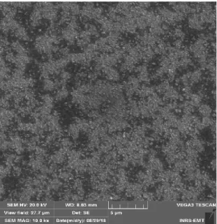
Figure 2.2 SEM image of FTO glass substrate. ...27
Figure 2.3 Band positions of different semiconductors in contact with aqueous electrolyte at pH 1. The conduction band (red colour) and the valence band (green colour) are presented along with the band gap in electron volts (eV) [7]. ...28
Figure 2.4 TEM image of TiO2 anatase nanoparticles. ...29
Figure 2.5 EDS spectra of the TiO2 anatase nanoparticles. ...29
Figure 2.7 Cross-sectional SEM image of mesoporous and scattering TiO2 layer: (a) low and (b)
high magnification. ...30
Figure 2.8 Various binding modes for a carboxylate unit on the TiO2 surface as an example of a metal oxide semiconductor: (a) monodentate (b) bidentate chelating (c) bidentate bridging [67]. ...31
Figure 2.9 UV-visible absorption of N719 dye molecule photosensitizers for DSSCs. ...31
Figure 2.10 Molecular structures of different dye molecule photosensitizers for DSSCs [55]. ....32
Figure 2.11 SEM image of Pt thin film layer on an FTO substrate. ...34
Figure 2.12 Polymorphs of carbon materials [80]. ...35
Figure 2.13 Electron transport across nanostructured semiconductor films: (a) and (c) CNT and (b) and (d) graphene composite electrodes [19]. ...37
Figure 2.14 TEM images of the MWCNTs: (a) low and (b) high magnifications. ...38
Figure 2.15 (a) DSSC fabrication steps and (b) a complete DSSC [83]. ...39
Figure 2.16 Schematics of diffraction of X-rays [84]. ...40
Figure 2.17 Electrons interact with a sample's atoms in the SEM [85]. ...40
Figure 2.18 Electron beams interact with a sample's atoms in the TEM [86]. ...41
Figure 2.19 Experimental setup for a typical AFM [91]. ...42
Figure 2.20 Experimental setup for a typical XPS [93]. ...43
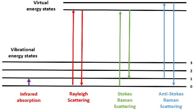
Figure 2.21 "Jablonski" style diagrams of different forms of energetic transitions in Raman scattering. ...44
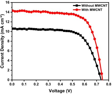
Figure 3.1 Current density-voltage curves of solar cells under simulated one sun at AM 1.5G (100 mW cm−2) fabricated using TiO 2 mesoporous films with (red circles) and without MWCNTs (black squares). ...54
Figure 3.2 Functional properties of DSSCs in cases with and without MWCNTs under a continuous one sun light irradiation as a function of soaking time: (a) J-V curves of DSSCs without MWCNTs; (b) J-V curves of DSSCs with MWCNTs; (c) Jsc (mA cm-2); (d) Voc (V); (e) FF (%); and (f) PCE (%). ...57
Figure 3.3 Transient Voc decay and obtained electron lifetime (τe): for cells without MWCNTs (a)
and (b) and cells with MWCNTs (c) and (d), measured at different times under one sun irradiation. ...59 Figure 3.4 Schematic of: (a) and (b) enhanced dispersion of TiO2 particles and preventing
agglomerating with MWCNT addition; (c) and (d) greater quantity of dye molecules are adsorbed to the highly porous morphology; (e) MWCNTs act as act good support and reinforcement for TiO2; (f) micro-crack formation in the photoanode because of intense light soaking and thermal
stress; (g) MWCNTs act as a strong conductive network, preventing charge recombination; (h) loss of electrical contact between the TiO2 particles and decrease in electron lifetime and
recombination resistance. ...60 Figure 3.5 Functional properties of DSSCs in cases with and without MWCNTs under a continuous indoor light irradiation as a function of soaking time: (a) J-V curves of DSSCs without MWCNTs; (b) J-V curves of DSSCs with MWCNTs; (c) Jsc (mA cm-2); (d) Voc (V); (e) FF (%);
and (f) PCE (%). ...62 Figure 3.6 Functional properties of DSSCs in cases with and without MWCNTs under a continuous UV light irradiation as a function of soaking time: (a) J-V curves of DSSCs without MWCNTs; (b) J-V curves of DSSCs with MWCNTs; (c) Jsc (mA cm-2); (d) Voc (V); (e) FF (%); and
(f) PCE (%). ...64 Figure 3.7 Schematic illustration of the band structure model for the TiO2 that forms deep
electronic traps. Under UV light illumination, the injected and photogenerated electron can be adsorbed through deep electron-donating sites. The electron in this site can then undergo direct recombination with a hole in the electrolyte. ...66 Figure 3.8 FESEM images of synthesized photoanodes: (a) without MWCNTs and (b) with MWCNTs at different magnifications before aging. Solid and dashed ovals highlight the agglomeration and porosity of the TiO2 particles, respectively. (c) Photoanode without MWCNTs
and (d) photoanode with MWCNTs after aging. ...67 Figure 3.9 (a) Schematic overview of a DSSC under Raman setup for Raman characterization; (b) a complete fabricated DSSC for Raman measurement; and (c) Raman spectra of cells in cases with and without MWCNTs at 514.5 nm before and after aging. ...70 Figure 3.10 (a)-(d): Electrochemical impedance spectroscopy analysis of fresh and aged cells without MWCNTs as a function of applied biases; (e) Bode phase of fresh and aged cells without MWCNTs; and (f) equivalent circuit of the transmission model. ...72
Figure 3.11 (a)-(d) Electrochemical impedance spectroscopy analysis of fresh and aged cells with MWCNTs as a function of applied biases; (e) Bode phase of the fresh and aged cells with MWCNTs; and (f) equivalent circuit of the transmission model. ...73 Figure 3.12 (a) Electrochemical impedance spectroscopy analysis of fresh and aged cells without MWCNTs and with MWCNTs for a bias of 450 mV; (b) charge-transfer resistance (Rct) as a function of applied bias in samples with and without MWCNTs, before and after aging; (c) and (d) Bode phase of fresh and aged cells in cases without and with MWCNTs, respectively; and (e) electron lifetime (τe) for cells without and with MWCNTs. ...74 Figure 4.1 Current density-voltage curves of solar cells under simulated one sun at AM 1.5G (100 mW cm-2) fabricated using TiO
2 mesoporous films with (red circles) and without MWCNTs (black
squares). ...82 Figure 4.2 PCE reduction (%) as a function of the thermal aging temperature of the two devices: TiO2 (black square) and TiO2-MWCNTs (red circle). ...83
Figure 4.3 Functional properties of DSSCs in cases with and without MWCNTs as a function of thermal aging time: (a) J-V curves of DSSCs without MWCNTs; (b) J-V curves of DSSCs with MWCNTs; (c) Jsc (mA cm-2); (d) Voc (V); (e) FF (%); and (f) PCE (%). ...85
Figure 4.4 FESEM images of the photoanodes without MWCNTs in different magnifications after thermal aging. Red arrows indicate cracks in the photoanode. ...87 Figure 4.5 FESEM images of the photoanodes with MWCNTs in different magnifications after thermal aging. ...88 Figure 4.6 High magnification FESEM images of the photoanodes with (a) 0.01 % wt and (b) 0.03 % wt of MWCNTs. Red arrows indicate MWCNTs. ...88 Figure 4.7 Transient Voc decay and obtained electron lifetime (τe): for cells without MWCNTs (a)
and (b) and cells with MWCNTs (c) and (d), measured after different thermal stress times. ...90 Figure 4.8 (a) and (b) EIS analysis of the fresh and aged cells without and with MWCNTs in biases at 300 and 450 mV respectively; (c) charge-transfer resistance as a function of applied biases before and after thermal aging; (d) Bode phase of the fresh and aged cells; (e) Mott-Schottky plots for fresh and aged cells without and with MWCNTs; and (f) equivalent circuit of the transmission model. ...92
Figure 4.9 Raman spectra of cells with and without MWCNTs at 514.5 nm before and after thermal aging. The insert shows a schematic overview of a DSSC under setup for Raman measurement. ...94 Figure 4.10 High-resolution XPS spectra of (a) TiO2 mesoporous films with and without MWCNTs,
before and after dye sensitization; (b) TiO2 mesoporous film before dye sensitization in the C 1s
region; (c) and (d) dye sensitized mesoporous film without and with MWCNTs in the C 1s region, respectively; (e) and (f) dye sensitized mesoporous film without and with MWCNTs in the N 1s region, respectively; (g) and (h) dye sensitized mesoporous film without and with MWCNTs in the S 2p region. ...96 Figure 5.1 (a) Photograph of the CuS-3G composite film. SEM images of CuS film with various concentrations of graphene at different magnifications: (b)-(c) bare CuS-0G; (d)-(e) CuS-3G; (f)-(g) CuS-10G. Red arrows indicate the microcrack areas. ... 106 Figure 5.2 EDS mapping of as-prepared CEs, (a) CuS and (b) CuS-3G nanocomposites. EDS spectra and measurement of chemical composition are taken from the red squared zones. ... 107 Figure 5.3 XRD pattern of as-prepared CuS-3G nanocomposites. ... 108 Figure 5.4 XPS plots of the CuS-3G composite film: (a) Survey; (b) Carbon; (c) Cu; (d) Auger Cu; and (e) Sulfur. ... 109 Figure 5.5 (a) Current density-voltage curves of the DSSCs under one sun simulated sunlight at AM 1.5G (100 mW cm-2) fabricated using different CEs. Variation of the photovoltaic parameters
of the corresponding devices: (b) PCE (%) and Jsc (mA cm-2); (c) Voc (mV) and FF (%). ... 111
Figure 5.6 (a) Transient Voc decay and (b) obtained electron lifetime (τe) for DSSCs fabricated
using different CEs. ... 112 Figure 5.7 Cyclic voltammogram for the standard three-electrode system using different CEs. ... 113 Figure 5.8 Current density-voltage curves of solar cells under one sun simulated sunlight at AM 1.5G (100 mW cm-2) fabricated using Pt and CuS-3G composite CEs. ... 114
Figure 5.9 Cyclic voltammogram of Pt and CuS-3G composite CEs. ... 115 Figure 5.10 Electrochemical impedance spectroscopy analysis of the Pt and CuS-3G composite CEs. ... 116 Figure 5.11 AFM images of: (a) Pt/FTO and (b) CuS-3G/Glass composite film. ... 118
Figure 5.12 Statistics (a) Jsc (mA cm-2); (b) Voc (mV); (c) FF (%); and (d) PCE (%) of 12 devices
as collected over 6 different batches. ... 119 Figure 1 Schéma d'une cellule solaire à jonction p-n [32]. ... 147 Figure 2 Sélection de points de repère PCE dans les DSSC [49]. ... 148 Figure 3 Schéma du principe de fonctionnement d'un DSSC et échelle de temps des processus au sein d'un appareil [54]. ... 150 Figure 4 Courbes densité / tension actuelles de cellules solaires sous un soleil simulé à AM 1,5G (100 mW cm-2) fabriquées à l'aide de films mésoporeux de TiO
2 avec (cercles rouges) et sans
MWCNT (carrés noirs). ... 153 Figure 5 Propriétés fonctionnelles des DSSC dans les cas avec et sans MWCNT sous irradiation continue d'un rayonnement solaire en fonction du temps de trempage (a) Courbes J-V des DSSC sans MWCNT, (b) Courbes J-V des DSSC avec MWCNT, (c) Jsc (mA cm-2); (d) Voc (V); (e) FF (%)
and (f) PCE (%). ... 154 Figure 6 Images FESEM de photoanodes synthétisées: (a) sans MWCNT et (b) avec des MWCNT à un grossissement différent avant vieillissement. Les ovales solides et en pointillés mettent en évidence l'agglomération et la porosité des particules de TiO2, respectivement. (c) photoanode
sans MWCNT et (d) photoanode avec MWCNT après vieillissement. ... 156 Figure 7 Illustration schématique du modèle de structure de bande du TiO2 formant des pièges
électroniques profonds. Sous illumination UV, les électrons injectés et photogénérés peuvent être adsorbés via des sites de donneurs d'électrons profonds. Ensuite, l'électron dans ce site peut subir une recombinaison directe avec un trou dans l'électrolyte. ... 158 Figure 8 Propriétés fonctionnelles des DSSC dans les cas avec et sans MWCNT en fonction du temps de vieillissement thermique (a) courbes J-V des DSSC sans MWCNT, (b) courbes J-V des DSSC avec MWCNT, (c) Jsc (mA cm-2); (d) Voc (V); (e) FF (%) and (f) PCE (%). ... 160
Figure 9 Décomposition transitoire de Voc et durée de vie électronique obtenue (τe): pour les cellules sans MWCNT (a et b) et les cellules avec MWCNT (c et d) mesurées après différents temps de contrainte thermique. ... 162 Figure 10 (a) Photographie du film composite CuS-3G. Images au MEB d'un film de CuS avec
Figure 11 Courbes densité / tension actuelles de cellules solaires sous une lumière solaire simulée à une AM 1,5G (100 mW cm-2) simulées à l’aide de CE composites Pt et CuS-3G. ... 165
LIST OF TABLES
Table 2.1. Properties of carbon allotropes [80]. ...36 Table 3.1. Functional parameters of DSSCs with and without MWCNTs. ...54 Table 4.1. Functional parameters of DSSCs with and without MWCNTs. ...82 Table 5.1. Functional parameters of DSSCs fabricated using different CuS-G nanocomposite CEs. ... 111 Table 5.2. Functional parameters of DSSCs with different Pt and CuS-3G CEs. ... 115 Table 5.3. Comparison of Rs (Ω) and Rct (Ω) calculated from EIS measurements of symmetric cell configuration of spin coated CuS-3G composite and Platinum CEs. ... 117
LIST OF ACRONYMS
PV Photovoltaic
DSSCs Dye sensitized solar cells PCE Photo conversion efficiency
UV Ultraviolet
CE Counter electrode
Pt Platinum
TCO Transparent conductive oxide MWCNTs Multi-wall carbon nanotubes SWCNTs Single-walled nanotubes
G Graphene
IEA International Energy Agency c-Si Crystalline silicon
a-Si Amorphous silicon
CIGS Copper indium gallium selenide
CIS Copper indium selenide
CdTe Cadmium telluride
QDSSCs Quantum dot sensitized solar cells
a-Si Amorphous silicon
CuS Copper sulfide
FTO Fluorine doped tin oxide
LUMO Lowest unoccupied molecular orbital HOMO Highest occupied orbital
ITO Indium-tin oxide
J-V Current-Voltage
Jsc Short circuit photocurrent density Voc Open circuit voltage
FF Fill factor
MPP Maximum power point
Rs Series resistance
Rp Parallel shunt resistance Pout Maximum obtainable power Pin Power of the incident light
V Voltage
J Current
ZnO Zinc oxide
SnO2 Tin(IV) oxide
TiO2 Titanium dioxide
CNTs Carbon nanotubes
𝜂LHE Light harvesting efficiency 𝜂inj Electron injection efficiency
𝜂reg Efficiency of dye molecules regeneration 𝜂col Charge collection efficiency
IPCE Incident photon to current efficiency
CPt Interfacial capacitance
Cµ Chemical capacitance
RTCO Charge-transfer resistance at the TCO and electrolyte interface CTCO Capacitance at the TCO and electrolyte interface
CCO Capacitance at the semiconductor layer and TCO contact RCO Resistance at the contact of the TCO and semiconductor Zd Impedance of the electrolyte
Rd Diffusion resistance of the redox species in the electrolyte
Cµ Chemical capacitance
τ𝑒 Electron lifetime
CB Conduction band
VB Valence band
XRD X-ray diffraction
SEM Scanning electron microscope
FESEM Field emission scanning electron microscopy EDS Energy-dispersive X-ray spectrometer
TEM Transmission electron microscopy SAED Selected area electron diffraction AFM Atomic force microscopy
XPS X-ray Photoelectron Spectroscopy 𝐸𝑏𝑖𝑛𝑑𝑖𝑛𝑔 Binding energy
𝐸𝑝ℎ𝑜𝑡𝑜𝑛 Photon energy
𝜙 Spectrometer work function
CV Cyclic voltammetry
QE Quantum efficiency
EQE External quantum efficiency IQE Internal Quantum Efficiency
MS Mott-Schottky
TMS Transition metal sulfides
eV Electron volt
MS Metal sulfides
CNTH Copper nitrate trihydrate
TAA Thioacetamide
"To truly transform our economy, protect our security, and save our planet from the ravages of climate change, we need to ultimately make clean, renewable energy the profitable kind of energy."
Introduction
In 2007, the Norwegian Nobel prize committee awarded for the first time the Nobel Prize for Peace to an important scientific consortium, the aim of which is to investigate and prove the rapid environmental and economic change in the earth’s climate, namely so-called “Global Warming”. The increase in the world’s energy demand due to the rapid growth of population has not only accelerated the depletion of the earth’s oil reserves, but has also resulted in environmental contamination and the greenhouse effect. Thus, the development of renewable and green energy sources is crucial towards a sustainable future. The American Recovery and Reinvestment Act in the United States has set a goal that greenhouse gas emissions should be reduced by 28% by 2020 [1]. In this context, the PV device that converts solar energy into electricity is a clean and renewable technology with considerable potential. However, this technology is not yet widely deployed; optimization of PV efficiency, long-term stability and cost reduction are the major challenges that hinder its widespread use [2–4]. Breakthrough developments in materials are needed to address these challenges. Since Gratzel and O’Regan first reported this new type of solar cell in 1991 [5], DSSCs have represented a promising solar technology due to appealing features such as a simple fabrication process, eco-friendly production, low production costs, colour choice and transparency [1,6]. Since then, this field of research has made considerable progress and is beginning to make significant inroads into solar energy [1,6].
DSSCs possess the ability to surpass the above mentioned challenges, in particular efficiency, stability and production cost for large-scale commercialization. During recent years, the research community has made significant advances on different components of DSSC including the anode, dye, electrolyte, and cathode, to improve PCE [1,6,7]. Progress in the design of device architecture has enabled the production of stable, reproducible cells and contributed to boosting the PCE up to ~ 14.7% [8]. However, there is still room for improvement, such as achieving long-term stability and decreasing production cost, both of which are crucial challenges for large-scale commercialization.
Various stability issues are generally associated with DSSCs, such as thermal stability as well as UV and visible light stability [9–13]. There are already interesting reports on improvement in the PV performance of DSSCs with the addition of carbon nano materials [14–19]. However, questions have been raised about whether this composite of carbon materials has any effect on the stability of DSSCs.
The CE, which is another important component in DSSCs, is generally made of Pt coated FTO [20–24]. While the overall fabrication cost of DSSCs is comparatively low, Pt and the TCO glass account for more than 40% of the total device cost [25–27]. Therefore, design and fabrication of TCO and Pt-free CEs for DSSCs without reducing electrocatalytic activity is the subject of much current interest in the field of DSSC research.
Objectives of the thesis
In the framework of this PhD project, DSSCs were fabricated in different configurations incorporating carbon nanomaterial composite structures in order to improve stability and decrease the production cost of the device.
Chapter 1, entitled ’Solar energy and solar cells’, is useful for understanding the basic concepts related to capturing solar energy and transforming it into electricity. The basic operational principle of PV is then discussed. An in-depth discussion on device structure and a theoretical description of the phenomena within the cell are also presented. The last section of this chapter provides the necessary foundations for the device’s investigation methods.
In Chapter 2, materials and experimental techniques, together with all of the used materials and experimental techniques for device fabrication and characterization, are described in detail.
The contribution of MWCNTs to the TiO2 anode is investigated in Chapter 3. The focus of this section is a comparison of the long-term stability of two devices made of (i) bare nanocrystalline TiO2 and (ii) MWCNTs-TiO2 composite anode, exposed to continuous visible and UV light irradiation.
subject of this section focuses on the effect on the thermal stability of DSSCs of incorporating MWCNTs.
Chapter 5 describes a simple, low temperature and solution-processable approach to preparing a composite film of CuS-G as a TCO and Pt-free CE for DSSCs.
CHAPTER
1
Solar energy and solar cells
During the last two decades, as a result of rapid development and industrialization, worldwide energy demands have shown a remarkable increase. All predictions indicate that this growth will continue by over 50% before 2030 [3,4]. According to the International Energy Agency (IEA) report, energy usage by nations with emerging economies, such as those in Southeast Asia, the Middle East, South America and Africa, will increase at an average annual rate of 3.2% while developed countries, including North America, Western Europe, Japan, Australia and New Zealand, will grow at an average rate of 1.1% [28,29]. Different forms of fossil fuels, including coal, oil and natural gas, contribute up to 80% of the world’s energy use [3]. A series of measurements of atmospheric CO2 levels demonstrate a relentless increase, year after year. The atmospheric CO2 concentration has risen from 300 to 380 ppm in the past 50 years. This unacceptable rise in the atmospheric CO2 level increases the earth’s temperature, with effects on global climate such as higher levels of atmospheric water vapor, changing weather patterns and rising sea levels from the melting of polar icecaps [30,31].
As a consequence, the limited availability of fossil fuels as a non-renewable energy source requires societies to make changes to their current energy management for sustainable living [3,4]. Energy management has led policy makers and industrialists to identify efficient means of energy shift to the utilization of new energy sources. Renewable energy sources have several advantages, such as being sustainable and nature friendly as well as their ability to reduce carbon emissions to the atmosphere [3,4]. An important decision faced by governments and businesses concerns which renewable energy source
consumption; and social impact [3,4]. Amongst various renewable energy sources, including solar, wind, hydroelectric, biomass, geothermal, hydrogen and ocean energy, solar energy is one of the cleanest and most abundant [2,28]. The amount of solar energy reaching the earth’s surface per second is more than the total energy that people have used since the beginning of time [28].
Solar energy is directly related to the light and heat generated by the Sun. The Sun can be considered as a black-body emitting radiation at 5500 K with a broad spectrum, stretching out from UV up to radio waves with a peak at 525 nm (2.36 eV), as shown in Figure 1.1 [32]. As can be observed, half of the solar spectrum falls in the infrared region (responsible for warming the Earth), 40% is in the visible region while the remaining 10% is in the UV region.
Figure 1.1 Solar irradiance spectrum (yellow: at the top of the Earth’s atmosphere; red: after passing through the atmosphere) comparison with spectrum of black body radiation at 5250°C (grey line) [32].
Solar energy can be captured through passive and active solar systems. Passive solar system merely collects the Sun’s energy without converting it into other forms: for example, maximizing the use of light and heat through green building design. Active solar
energy technology refers to the converting of solar energy into other forms of energy that can be classified into three groups: (i) solar cell; (ii) chemical energy; and (iii) solar thermal [2,28,33].
1.1 Photovoltaics
The French scientist, Edmond Becquerel, first discovered the PV effect in 1839 [34]. The solar cell is an electrical device that converts the energy of sunlight directly into electricity. This subject has created a new road for renewable energy sources with the potential to replace a significant percentage of fossil fuels. The conversion of solar energy into electricity by a solar cell is based on three primary mechanisms: (i) the absorption of a photon and generation of a carrier; (ii) carrier separation; and (iii) charge-carrier collection [35,36].
PV devices mainly exploit a semiconductor material that works as a light absorber. As can be seen from Figure 1.1, the region between 400 and 1100 nm has the highest photon density in the solar spectrum. Therefore, an ideal light absorber (semiconductor) is a material that can absorb sunlight between 400 and 1100 nm. Upon absorption of photons with energy equal or greater than the band gap of the semiconductor (hν ≥ Eg), an electron/hole pair is generated. The electron and hole can then be effectively separated and diffused toward the n-type semiconductor and the p-type semiconductor, respectively (Figure 1.2) [32]. Electrons flow through an external circuit and generate an electric current.
1.2 Classification of solar cells
In 1883, Charles Fritts first reported the fabrication of a complete solar cell by a sandwich structure, consisting of selenium and gold, whose PCE reached less than 1% [37]. In 1954, Darly Chapin, Calvin Fuller and Gerald Pearson built the first silicon-based solar cell at the Bell Telephone Laboratories, reporting a PCE as high as 6% [38]. From that time until now, researchers have been trying to develop a simple structure and low cost technology by applying new materials, approaches and concepts. Martin Green categorized solar cells in three different generations based on the nature of the material, PCE, and cost effectiveness [39]. Figure 1.3 graphically shows energy conversion efficiency ranges and possible module production costs per unit area for the three generations of technology [39].
Figure 1.3 Efficiency and production cost projections for three generations of solar cells [40].
1.2.1 First generation
First generation PV is based on extremely purified crystalline silicon (c-Si). This generation features a quite high conversion efficiency (~24%) thanks to a broad absorption spectral range. Unfortunately, manufacturing processes that are applied to
growing highly pure c-Si are inherently expensive, thus raising the cost of devices. Thus, first generation is characterized by high production costs as well as moderate efficiency [32,39]. The first generation of solar cells consists of monocrystalline and polycrystalline silicon solar cells. The value of conversion efficiency for monocrystalline (~ 24%) is higher than polycrystalline silicon (~ 20%) solar cells, due to high rate exciton recombination at the grain boundaries [32,39]. However, production of a multicrystal wafer is easier and cheaper compared with polycrystalline.
First generation solar cells are also known as conventional and traditional cells. Solar cells based on the II-IV and III-V groups are also classified under the first generation category. First generation PVs account for 86% of account for 86% of the solar cell market due to high conversion efficiency and a large amount of purified Si production by well-developed semiconductor industries.
1.2.2 Second generation
Second-generation solar cells, which were introduced to reduce the production cost of first generation whilst maintaining the PCE, are based on thin film technology. There is no doubt that, while second generation PVs certainly address the high production cost issue of first generation PVs, their efficiencies are lower than first generation [32,39]. Second generation are more applicable to purposes such as windows, cars, and building integrations because there are no fingers in front. As an advantage of solar cells, these thin films can also be grown on flexible substrates and in large areas, up to 6 m2 [41]. The most common second generation solar cells available on the market are [41]:
Amorphous silicon (a-Si), with 10.1% conversion efficiency
Copper indium gallium selenide (CIGS), with 19.9% conversion efficiency Copper indium selenide (CIS) , with 12.5% conversion efficiency
1.2.3 Third generation
In recent years, third generation PVs have been designed to combine the advantages of first and second generation devices. Any cells that are not grouped into first and second generations belong to third generation PVs, including polymer (or organic) solar cells, DSSCs, quantum dot sensitized solar cells (QDSSCs) and perovskite solar cells. This generation can perhaps represent the future of solar cell technology with a higher PCE and lower cost of device fabrication. Thermodynamics show that the limit on the conversion of sunlight to electricity for a single junction solar cell is 31%. This so-called Shockley-Queisser limit assumes that absorption of an individual photon results in the formation of a single electron-hole pair and that all photon energy in excess of the energy gap is converted into heat [39,42]. The best record and history of PCE of all types of solar cells is presented in Figure 1.4 [43].
Figure 1.4 Best research-cell reported by the National Renewable Energy laboratory [43].
During the last three decades, DSSCs have attracted great attention in both industry and the scientific community working in the solar cell field as a possible alternative to the conventional crystalline silicon and thin-film solar cells, due to the following selling points [6,42]:
Much lower investment costs compared with conventional and traditional PV technologies
Low production cost (short energy payback time [<1 year])
Relatively better performance than competitors under real outdoor conditions at diffused light and higher temperatures
Design options, such as transparency and multicolor opportunities Ability to outperform competitors for indoor applications
Flexibility and light weight.
1.3 Dye-sensitized solar cells (DSSCs)
1.3.1 Brief history
The dye-sensitization process on wide band gap semiconductors, including ZnO and SnO2, was reported in the late 1960s [44,45]. Gerischer studied the effect of dye adsorption on the stability of large band gap semiconductors under a visible region [44]. Most of these works reported fundamental concepts and novel materials used in DSSCs, such as dye-sensitization of semiconductors, electrolyte redox chemistry and electron-transfer processes [46,47]. The obtained cells were characterized with low conversion efficiencies (1-2%) due to the poor dye anchorage on the semiconductor surface and weak light absorption [45,48].
Since 1991, DSSCs have attracted great attention in the solar cell field, following the breakthrough work by O’Regan and Gratzel who introduced the mesoporous structure of the TiO2 and a tris (2, 2’-bipyridyl 4, 4’-carboxylate) ruthenium (II) dye as a light harvester, and reported a record PCE of around 8% [5]. Subsequent to this pioneering work, researchers have been racing to further improve both the PCE and stability of DSSCs for large scale commercialization by optimizing the different components (metal oxide, dye, electrolyte and CE) of the device (Figure 1.5) [49]. Recently, a PCE greater than 14% has been reported for DSSCs [8]. Although this is still lower than the PCE of the Si based
efficiency in diffuse sunlight or cloudy conditions; and (ii) performance is less sensitive to the incident angle of light radiation [6,42].
Figure 1.5 Selected PCE landmarks in DSSCs [49].
1.3.2 Cell architecture
DSSCs are made in a sandwich configuration of different materials that are trapped between two pieces of conducting glass. A schematic of a complete cell is presented in Figure 1.6. The main components of the DSSC are: a semiconductor, dye, transparent electrode, an electrolyte and a CE. The photoanode is constituted of a 10-20 µm thick layer of a wide band gap metal oxide semiconductor (usually TiO2, ZnO and SnO2) deposited on a transparent conducting oxide substrate. Among different types of semiconductors, TiO2 nanostructure is the most efficient material to be used as a photoanode. A TiO2 photoanode is composed of two different layers: (i) an 8-14 µm mesoporous film of 20 nm sized TiO2 nanoparticles called the “active layer”; and (ii) a 4-6 µm layer of 200-400 nm sized nanoparticles called the “scattering layer”. Dye molecules serve as antennae to harvest the sunlight (photons). The light enters the device from the photoanode side, so that good transparency of the substrate is necessary. The CE is
typically made with a platinized (5-10 nm Pt thin layer) transparent conducting glass. The space between the dye sensitized photoanode and the CE is filled by a liquid electrolyte [5,50–52].
1.3.3 Basic Operating Principle of DSSCs
DSSCs are quite different from conventional p-n junction solar cells by their basic construction and the physical processes behind their operation. The typical configuration of DSSCs combines two solid and liquid phases, while other solar cells are based on the solid phase [5,6,36,50–52]. All the components and a complete cycle to conversion of light into electrons in DSSCs are shown in Figure 1.6. The overall PCE of DSSCs can be evaluated based on three factors: (𝜂 = 𝜂 abs+𝜂 inj+𝜂 coll) [53]. One cycle of a DSSC operation is completed in five steps, as described below:
Light Absorption
In DSSCs, sensitizer molecules are adsorbed on the surface of metal oxide semiconductors (e.g., TiO2 and ZnO) and act as light harvesters. The ideal sensitizer should meet several requirements. These include: (i) the sensitizer should be able to harvest more light of the solar spectrum; (ii) the sensitizer must carry a carboxylate or phosphonate group to make a chemical bounding to the surface of the semiconductor; (iii) the lowest unoccupied molecular orbital (LUMO) of the sensitizer must be higher than the conduction band of the semiconductor; (iv) the highest occupied orbital (HOMO) of the sensitizer must be sufficiently low to accept electron donation from an electrolyte; and (v) there should be chemical and thermal stability in the electrolyte media and during exposure to solar radiation [6]. Due to the absorption of light, the dye molecule is excited from the ground state (S) to the excited state (S*). In this condition, an electron jumps from the HOMO to the LUMO of the dye molecule (Step 1) [6,36,42].
Charge separation
Charge separation in DSSCs is fundamentally different from the p-n junction solar cell. Due to the concentration difference between the p and n type semiconductor in a conventional photovoltaic built on a p-n junction, the holes move to the n region and the electrons to the p region. In DSSCs, the excited electron must successfully inject from the LUMO of the dye molecule to the conduction band of the semiconductor (Step 2). The electron injection typically occurs on a time scale of femtoseconds. The next step for charge separation is hole transfer from the HOMO to the electrolyte (Step 3) [6,36,42]. After transferring the hole from dye to electrolyte (reducing the dye), the positive charge is now moved to the redox couple and the negative charge, or electron, is injected into the conduction band of the semiconductor, which creates a charge separation between the hole and the electron [36,50,55].
In metal based dyes, the electron excitation occurs via a metal to ligand charge transfer mechanism. Under the absorption of photons, electrons are shifted from the metal part of the dye molecules to the ligand. This shifting of the electron leads to oxidation of the metal and a reduction of ligands. The dye molecules are covalently bonded to the surface atom of the metal oxide (e.g. TiO2, ZnO, SnO2) via carboxylic groups in the ligand species. This
bonding leads to significant overlapping between the LUMO level of the dye and the conduction band of the metal oxide that is necessary for electron injection from the LUMO level of the excited dye molecules to the conduction band of the metal oxide semiconductor [56,57].
Charge-carrier transport
After charge separation, the hole and the electron travel through the electrolyte (Step 3) and mesoporous metal oxide layer (Step 4), respectively. DSSCs are majority carrier devices where electrons and holes are separated into two chemical phases. Although many theoretical and experimental investigations have been carried out to understand the exact mechanism of electron transport through the mesoporous metal oxide, diffusion via a trapping/detrapping mechanism along localized energy levels below the conduction band edge seems the most realistic [36,50,55]. Under illumination, the injected electrons to the conduction band of metal oxide particles generates a potential gradient within the particles and appears to be the main driving force for transport in the mesoporous film [42]. After diffusing in the nanocrystalline semiconductor network to the conductive coating of the substrate, electrons can be transferred to an external circuit.
After the injection of the electron from the LUMO of the excited dye molecule to the conduction band of the semiconductor, the hole is left in the HOMO of the oxidized dye molecules. For current generation, the dye must be reduced by taking the electron from the redox couple electrolyte. The oxidized electrolyte then diffuses to the CE and is reduced back to the iodide by the collected electrons from the external circuit (Step 5) [36,50,55].
Recombination processes
The main source of the losses in the performance of DSSCs is non-radiative carrier recombination [42]. This reaction can occur via two channels: in the conduction band of mesoporous metal oxide and in the LUMO of the excited dye. The first process is the recombination of electrons in the conduction band of the semiconductor with acceptors in the electrolyte (Step 6). The probability of occurrence of this process is higher compared
oxide nanoparticles. Recombination can occur both at the semiconductor/electrolyte interface and at the part of the conducting substrate that is exposed to the electrolyte [42,55]. However, electron back reaction at the conducting substrate/electrolyte interface can be suppressed by deposition of a compact blocking layer [42]. Recombination of electrons with oxidized dye molecules is another possible reaction (Step 7). This reaction competes with the regeneration process of dye molecules with electron transfer from the conduction band of the semiconductor to oxidized dye molecules, which usually occurs on a time scale of about 1 µs [42]. The last recombination process takes place in excited dye molecules by re-combining of the electron in the LUMO with a hole in the HOMO of the dye molecules (step 8). This recombination process competes with the process of electron injection into the conduction band of the semiconductor that occurs in the femtosecond time range and which is much faster than the electron recombination [6,42,50,55].
1.4 Characterizations of photovoltaic performance
The most important measurement of a solar cell is the current density-voltage (J-V) characterization curve under standard conditions (temperature, spectral irradiance, total irradiance) to report the performance of the cells [36]. In order to be able to compare performances of solar cells, the J-V curve is measured under standard illumination conditions (see the standard test conditions section). The J-V characteristics are monitored under illumination or dark conditions by applying an external potential (altered from Jsc to Voc) between two electrodes. Since no oxidized dye is present in dark conditions, the dark current gives information about the electrons moving in reverse, from the semiconductor nanoparticles to the oxidized species of the redox couple, which is a recombination of the oxidized redox species [1,6,36]. An example of a J-V curve under illumination is shown in Figure 1.7.
Figure 1.7 Typical current-voltage curve of a photovoltaic cell.
1.4.1 Short circuit photocurrent density
Short circuit photocurrent density (Jsc) is the photocurrent divided by the active area of the device (mA cm-2) when the device is short-circuited or, in other words, when the external output voltage is zero. In DSSCs, Jsc depends on several factors such as: the light intensity; electron generation and injection efficiency; recombination resistance; and the efficiency of charge transport [35,36]. Graphically, Jsc is determined by the intersection with the y-axis (when V = 0), as shown by the J-V curve.
1.4.2 Open circuit voltage
The open circuit voltage (Voc) is the maximum voltage obtained from a solar cell under open circuit conditions when no external load is connected. Graphically, Voc is determined by the intersection with the x-axis (when J = 0). For DSSCs, the Voc is given by the difference between the Fermi level of the semiconductor and the redox potential of the electrolyte [58]. 0.0 0.1 0.2 0.3 0.4 0.5 0.6 0.7 0.8 0 -2 -4 -6 -8 -10 -12 -14 -16 JMP Jsc VMP Voc Curr en t De ns ity ( mA cm -2) Voltage (V) MPP
where ECB is the conduction band edge energy level, NCB is the effective density of states in the semiconductor, and q is the elementary charge of the electrons. For a defect-free semiconductor material β=1 [58]. n is the number of electrons in the conduction band of the semiconductor that is determined by the balance between electron injection and electron recombination [58].
1.4.3 Fill Factor
The fill factor (FF), which is a parameter related to the maximum power point (MPP), is often described as a measure of the “squareness” of the J-V curve. The general formula for electric power is P = J×V. The FF value is determined by the ratio of the current and voltage at the MPP (JMP-VMP) and the parameter of the cell (Jsc-Voc), with a value between 0 and 1 [1,6].
𝐹𝐹 =J𝑀𝑃 × V𝑀𝑃
J𝑠𝑐× V𝑜𝑐 (𝐄𝐪𝐮𝐚𝐭𝐢𝐨𝐧 𝟏. 𝟐) The FF is dependent on the Rs and Rp of the solar cell. Rs in a solar cell is the result of contact resistance and charge transfer resistance that reduces the FF affecting the maximum power output. To obtain a higher FF, an improvement in the Rp is required (Figure 1.8) [1,6,59].
Figure 1.8 Evolution of simulated J-V curves with the change of (a) overall series resistance and (b) parallel shunt resistance [59].
1.4.4 Efficiency
The overall performance of a solar cell is evaluated by the solar-to-electrical energy conversion efficiency (𝜂), which is determined by the ratio of the maximum obtainable power (Pout) to the power of the incident light (Pin) [1,6,36].
η =P𝑜𝑢𝑡 P𝑖𝑛 =
J𝑠𝑐× V𝑜𝑐× 𝐹𝐹
P𝑖𝑛 (𝐄𝐪𝐮𝐚𝐭𝐢𝐨𝐧 𝟏. 𝟑)
1.4.5 Incident photon to current conversion efficiency
The incident photon to current conversion efficiency (IPCE) gives information about the efficiency of the solar cell in converting sunlight at a particular wavelength into an electrical current. In DSSCs, the IPCE factorized into different parameters such as light harvesting efficiency (𝜂LHE), electron injection efficiency (𝜂inj), the efficiency of dye molecule regeneration (𝜂reg), and photo-generated charge collection efficiency (𝜂col) [60].
η𝐼𝑃𝐶𝐸 = η𝐿𝐻𝐸× η𝑖𝑛𝑗× η𝑟𝑒𝑔 × η𝑐𝑜𝑙 (𝐄𝐪𝐮𝐚𝐭𝐢𝐨𝐧 𝟏. 𝟒)
The IPCE is also defined as the ratio of the output electrons to the incident photons at a particular wavelength (λ): η = Output electrons (λ) Incident photons (λ)= 1240 × J𝑠𝑐(cmmA2) λ (nm) × P𝑖𝑛(mW cm2) (𝐄𝐪𝐮𝐚𝐭𝐢𝐨𝐧 𝟏. 𝟓)
where Pin is the input power and λ is the illumination wavelength [1,60].
The IPCE can be used as a useful technique to cross-check the result obtained with the J-V measurements. The Jsc is the integrated sum of the IPCE (λ) measured over the entire solar spectrum:
J𝑠𝑐(λ) = ∫ 𝐼𝑃𝐶𝐸 ∞ 0
(λ)I𝑠𝑢𝑛 (λ)𝑑λ (𝐄𝐪𝐮𝐚𝐭𝐢𝐨𝐧 𝟏. 𝟔) where I𝑠𝑢𝑛 (λ) is the incident irradiance as a function of the wavelength.
1.4.6 Standard test conditions
To compare photovoltaic performance, solar cells are measured under a set of standard test conditions: (i) the temperature of the cell should be 25°C; (ii) the total input power density of solar radiation must be 100 mW cm-2 [35,36]. All the photovoltaic parameters (PCE, FF, Jsc, and Voc) depend on the temperature and the intensity of illumination light. The sun’s spectral power distribution is characterized as air mass (AM), which measures the reduction in the spectral content and intensity of solar radiation as it passes through the atmosphere, mainly caused by the scattering and absorption of the light by air molecules and dust particles. The air mass number is given by [35,36]:
Air mass = 1
𝐶𝑜𝑠 𝜃 (𝐄𝐪𝐮𝐚𝐭𝐢𝐨𝐧 𝟏. 𝟕) where 𝜃 is the angle of incidence (Figure 1.9).
Figure 1.9 Typical illustration of air mass.
The standard for comparing solar cell performance is a spectrum normalized to a total power density of 100 mW cm-2, AM1.5 at 𝜃 = 48.2°. AM0 is then the value for the solar irradiation just above the Earth’s atmosphere where the radiation intensity is about 130 mW cm-2. AM1 corresponds to the shortest possible path length when the sun radiation is coming at an angle of 0° [35,36].
1.4.7 Electrochemical impedance spectroscopy
Electrochemical impedance spectroscopy (EIS) is a powerful tool for investigating the kinetics of charge transport and recombination in DSSCs. EIS is widely used in these fields because of its sensitivity to electron diffusion and recombination at the interfaces of the metal oxide/electrolyte, CE/electrolyte and TCO/electrolyte interface [61,62]. Moreover, EIS is a non-destructive technique for analyzing the degradation mechanisms of DSSCs, including electron transport resistance in the different interfaces [63].
The equivalent circuit of a complete DSSC is represented in Figure 1.10 (a) [59]. The key parameters of the equivalent circuit are:
Mesoporous TiO2 film is the most characteristic element of the transmission line; its electron transport resistance is Rt=rtL (L as the thickness of the nanoporous TiO2). The interfacial charge recombination resistance and the chemical capacitance in the nanoporous film are Rct= rct/L and Cµ= cµL, respectively. Charge-transfer resistance Rct and the interfacial capacitance CPt at the Pt CE and
the electrolyte interface are other important elements in the DSSC model. RTCO is the charge-transfer resistance at the TCO and the electrolyte interface. CTCO is the capacitance at the exposed TCO and the electrolyte interface. Rs is the sheet resistance of the TCO.
The capacitance of the semiconductor layer and the TCO contact is CCO. RCO is the resistance at the contact of the TCO and the semiconductor layer. Zd and Rd are the impedance and diffusion resistance of the redox species in the
electrolyte.
Under high-illumination intensity, due to the electron excitation and injection from dye molecules to the semiconductor nanoparticles, the transport resistance becomes negligible and the equivalent circuit can be simplified (Figure 1.10b) [59].
Figure 1.10 (a) General transmission line model of DSSCs and (b) simplified model at high illumination intensities [59].
The Nyquist plots of the complete DSSC can be represented in three semi-circles, as shown in Figure 1.11.
The semi-circle that appears at high-applied potentials is related to the charge transfer resistance at the CE/electrolyte interface.
The second semi-circle at medium-applied potentials represents the behaviour of the charge carrier at the metal oxide/dye/electrolyte interface.
The third semi-circle at low-applied potentials reports information that represents the response of the diffusion resistance of the electrolyte.
Information can be obtained about the Rs of the complete cell from the distance between the origin and the first semi-circle.
Figure 1.11 Typical impedance spectra (Nyquist plot) of a complete DSSC.
EIS is a well-established electrochemical method designed to study the electron lifetime (τ𝑒) of DSSCs. This measurement can be performed by two different methods:
The second semi-circle of the Nyquist plots reports some information about the chemical capacitance, charge transfer and recombination resistance of the injected electron to the conduction band of the semiconductor. Based on Equation 1.7, these parameters allow the calculation of the electron lifetime at each applied bias [59,61,64].
τ𝑒 = R𝑐𝑡× C𝜇 (𝐄𝐪𝐮𝐚𝐭𝐢𝐨𝐧 𝟏. 𝟖) The EIS results can also be represented in Bode plots in terms of phase angle
versus frequency (Figure 1.12). The electron lifetime can be evaluated with Bode plots by using the following equation [65]:
τ𝑒 = 1 2 × 𝜋 × 𝑓𝑚𝑎𝑥 (𝐄𝐪𝐮𝐚𝐭𝐢𝐨𝐧 𝟏. 𝟗) 0 4000 8000 12000 16000 20000 24000 0 -2000 -4000 -6000 -8000 -10000 -12000 Rs CE / electrolyte
interface Electron diffusion
Z''(
Ohm)
Z' (Ohm)
Figure 1.12 Typical Bode plots of a complete DSSC. 0.01 0.1 1 10 100 1000 10000 100000 0 -20 -40 -60 -80 q (d eg ) Frequency (Hz)
“Experiments are the only means of knowledge at our disposal. The rest is poetry, imagination.”
CHAPTER
2
2
Materials and experimental techniques
This chapter includes a description of the materials, cell fabrication procedures and device characterization by various techniques.
2.1 Materials
2.1.1 Transparent conductive oxide electrode
A schematic representation of the structure of DSSC is shown in Figure 2.1 [55]. In the case of the front side, the substrate should be highly transparent in the visible-IR region, but blocking the UV light. On the other hand, the backside of the substrate should have a high reflection to enhance light absorption by reflecting back the transmitted light into the dye. Moreover, other requirements for a good DSSC substrate are low sheet resistance, high transparency, thermal stability up to 450-500 oC, and ability to prevent impurities such as water and oxygen from entering into the cell. TCO-coated glass is generally used as the substrate for DSSCs. Indium doped-tin oxide (ITO) is one of the most well-known TCO materials for solar cell application, but it has a low thermal stability (ITO’s sheet resistance also increases with temperature). Fluorine-doped tin oxide (FTO)-coated glass is commonly used as the TCO substrate for DSSCs (around 10 Ω cm-2). Other materials developed for working as a substrate for DSSCs include plastic foils and metal sheets to overcome some of the disadvantages of glass, such as fragility, rigidity, heavy weight and a high price. Conductive plastics are lightweight and flexible but they have low temperature tolerance, high Rs (around 60 Ω cm-2), and uncertainties considering the oxygen and water penetration. While metals are also mechanically robust, their main problem is corrosion behavior when in contact with an electrolyte. Stainless steel and
titanium have shown enough chemical stability in the iodine electrolyte, but their price is higher than glass [32,35,36,66].
In the present work, FTO glass substrate has been used for solar cell fabrication with sheet resistance in the range of 10-15 Ω cm-2 (Figure 2.2).
Figure 2.2 SEM image of FTO glass substrate.
2.1.2 Anode
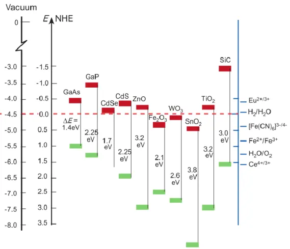
The DSSC revolution actually started from the application of a mesoporous anode with a high surface area. The primary role of the mesoporous layer is to provide adequate surface area for loading sufficient amounts of dye molecules since monolayers of semiconductors lead to an intrinsic limitation. A monolayer of dye bound to the surface can inject electrons into the semiconductor. During the last few years, different semiconductors have been used for the working electrode of DSSCs. Figure 2.3 illustrates the band positions of several semiconductors [7]. The conduction band edge of the metal oxide semiconductor should be below the LUMO level of the dye. Metal oxide semiconductor must be chemically stable when in contact with the electrolyte, has a lattice structure suitable for dye bonding and be available in nanostructured form to enable high enough dye loading [6,50,55].
TiO2 is the most efficient material to be used as photoanode, with a large band gap (3-3.2 eV). The thickness of the electrode is determined by the absorption coefficients of the dye molecules and electron diffusion length of the electrodes. To produce high-performance DSSCs, electrodes are prepared from small nanoparticles (25 nm, 10-18 micron thickness) and a scattering layer consisting of large nanocrystalline TiO2 particles (250-300 nm, 5-10 micron thickness) [6,7,32,50].
Figure 2.3 Band positions of different semiconductors in contact with aqueous electrolyte at pH 1. The conduction band (red colour) and the valence band (green colour) are presented along with the band gap in electron volts (eV) [7].
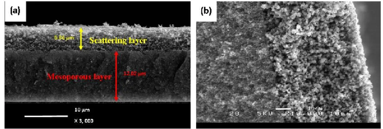
In this work, commercially available paste of TiO2 nanoparticles is used as a metal oxide semiconductor. TiO2 paste (18 NR-T) contains highly dispersed and stable anatase nanoparticles of 20 nm size as an active layer (Figure 2.4-2.6). The scattering paste (WER2-O) contains 150-250 nm sized anatase particles. These pastes are provided by Dyesol (Australia). TiO2 nanoparticle paste is deposited on TCO glass substrates by the doctor blade method. Figure 2.7 shows the anode structure of the DSSC.
Figure 2.4 TEM image of TiO2 anatase nanoparticles.
Figure 2.5 EDS spectra of the TiO2 anatase nanoparticles.
0 1 2 3 4 5 6 7 8 9 0 500 1000 1500 2000 2500 Ti O C Ti Ti Cu Cu In te ns ity (Co un ts ) Energy (keV)
Figure 2.6 XPS spectra of the TiO2 anatase nanoparticles.
Figure 2.7 Cross-sectional SEM image of mesoporous and scattering TiO2 layer: (a) low and (b) high
magnification.
2.1.3 Sensitizers
Unfortunately, because of their wide band gap, metal oxide semiconductors absorb only the UV part of solar emission, which represently about 4-5% of the total. To optically enhance the light absorption in the visible-infrared region, dye molecules are chemically
0 100 200 300 400 500 600 700 Ti 2s O 1S Ti 2P In te ns ity (a .u .)
Binding energy (eV) C 1S
surface needs to be stable. For a strong linking of the dye to the semiconductor surface, most dyes have an anchoring group that reacts with the semiconductor surface and creates a chemical bond, over which charge transfer takes place. Usually commercially available dyes, such as N719 and black dye, have a carboxylic acid anchoring group that can coordinate to the oxide surface of the semiconductor in three different modes, namely unidentate, chelating and bridging bidentate, as shown in Figure 2.8 [67].
Figure 2.8 Various binding modes for a carboxylate unit on the TiO2 surface as an example of a
metal oxide semiconductor: (a) monodentate (b) bidentate chelating (c) bidentate bridging [67].
The most efficient and stable dye molecules in use are ruthenium (II) based dyes. However, they come with several drawbacks, especially a high cost and a limited amount of noble metals (Figure 2.9). The different forms of ruthenium-complex dye molecules that are commonly used in DSSCs, and which provide particularly high PCE, are shown in Figure 2.10 [55].
In this work, Ru (II) based dye coded N719 is applied as the light harvester.
400 450 500 550 600 650 700 Absorpt ion (a. u .) Wavelength (nm)
![Figure 1.3 Efficiency and production cost projections for three generations of solar cells [40]](https://thumb-eu.123doks.com/thumbv2/123doknet/5004612.124689/33.918.233.717.501.863/figure-efficiency-production-cost-projections-generations-solar-cells.webp)
![Figure 1.4 Best research-cell reported by the National Renewable Energy laboratory [43]](https://thumb-eu.123doks.com/thumbv2/123doknet/5004612.124689/35.918.111.812.513.885/figure-best-research-reported-national-renewable-energy-laboratory.webp)
![Figure 1.6 Schematic of the working principle of a DSSC and time scale of the processes within a device [54]](https://thumb-eu.123doks.com/thumbv2/123doknet/5004612.124689/38.918.160.791.516.948/figure-schematic-working-principle-dssc-scale-processes-device.webp)
![Figure 2.10 Molecular structures of different dye molecule photosensitizers for DSSCs [55]](https://thumb-eu.123doks.com/thumbv2/123doknet/5004612.124689/58.918.126.798.147.682/figure-molecular-structures-different-dye-molecule-photosensitizers-dsscs.webp)
![Figure 2.18 Electron beams interact with a sample's atoms in the TEM [86].](https://thumb-eu.123doks.com/thumbv2/123doknet/5004612.124689/67.918.331.608.598.878/figure-electron-beams-interact-sample-s-atoms-tem.webp)