OATAO is an open access repository that collects the work of Toulouse
researchers and makes it freely available over the web where possible
Any correspondence concerning this service should be sent
to the repository administrator:
[email protected]
This is an author’s version published in:
http://oatao.univ-toulouse.fr/24518
To cite this version:
Saïdi, Hanane and Boujmil, Mohamed Fethi and Durand, Bernard
and Lazzari,
Jean-Louis and Bouaïcha, Mongi Elaboration and characterization of
CuInSe2thin films using one-step electrodeposition method on silicon substrate
for photovoltaic application. (2018) Materials Research Express, 5 (1). 016414.
ISSN 2053-1591
https://doi.org/10.1088/2053 1591/aaa604
Elaboration and characterization of CulnSe
2
thin films using one
step electrodeposition method on silicon substrate for
photovoltaic application
H Saï di 1, MF Boujmil1, B Durand 2, J-L Lazzari3 and M Bouaïcha 1 G
1 Laboratoire de P hotovoltàique, Centre de Recherches et des Technologies de l'tnergie, Technopole de Borj Cédria, Université Tunis El
Manar, BP95, Hammam Lif, 2050Tunis, Tunisia
1 CIRIMAT,CNRS, INPT, Université de Toulouse, 118, Route de Narbonne,F 31062Toulouse cedex9,France
3 A ix Marseille Univ, CNRS, CINaM (Centrelnterdisciplinaire de Nanoscience de Marseille), Case 913, Campus de Luminy, F 13288
Marseille cedex 9, France E mail: [email protected]
Keywords: bifacial solar œll, CIS/c Si, electrodeposition, galvanostatic mode, rapid thermal annealing, heterojunction solar cell
Abstract
Bifacial solar cells combining a heterojunction cell on the upper side and crystalline silicon ( c-Si) homoj unction on the backside are very interesting devices to a more efficient use of the solar radiation. Cu(In,Ga)Sei(n)/ c-Si(p )/ c-Si(n +) or CulnSei(n)/ c-Si(p )/ c-Si(n +) are very attractive heteroj unctions to reach this target. In this work, a novel attempt has been made to grow CulnSe2 thin films on p-Si (100) substrate using one-step electrodeposition route with galvanostatic mode. The as-deposited samples were amorphous by nature which implies a rapid thermal annealing step. The effect of annealing temperature on the structural, morphological, optical and electrical properties of the fabricated hetero-structure CulnSe2/c-Si (100) was investigated by x-ray diffraction (XRD), scanning electron microscopy, energy dispersive spectroscopy (EDS) and UV-visible spectroscopy. XRD indicates that CulnSe2 films having single phase chalcopyrite with tetragonal crystal structure are obtained at 3 50 °C. Values of energy band gap of films at various annealing temperature were estimated to be in the range 0.94-1.01 eV. The optical parameters such as refractive index
n(>.)
andextinction coefficient
k(>.)
were estimated using an appropriate optical model. The AM 1.5 currentdensity-voltage characteristic of the fabricated Al/CulnSe2/ c-Si (100) hetero-junction solar cell exhibits a short-circuit current density Ise of 4.06 mA cm 2, an open circuit voltage V0cof0.28 V, a fill factor FF of 36. 72% and a solar conversion efficiency
17
of 0.41 %.1. Introduction
One of the main objectives of scientific research in photovoltaic (PV) is to explore new processing techniques and new materials which assure three criteria; scalability, low-cost and manufacturability. The efficiency of mono-crystalline silicon PV cells has remained nearly unchanged for two decades (current record efficiency being 25.8%) while the module stability is guaranteed over 20 years [l]. A second generation of solar cells based on heterojunction thin film technologies has been developed using scalable manufacturing techniques, non expensive substrates and alternative materials. Among them copper indium gallium diselenide (CIGS) has shown its full potential in this field [2, 3) since ithas a high optical absorption coefficient(~l05 cm 1
), direct band gap and long term optoelectronic stability [ 4, 5). CIGS based solar cells (with record efficiency of 22.6%) are now a major candidate for application in building integrated photovoltaics. Correspondingly, silicon HIT heterostructure solar cells, as composed of a mono thin crystalline silicon (c-Si) wafer stacked by ultra-thin amorphous silicon ( a-Si) layers, have reached a record efficiency as high as 26.6%. This opens theway for new concepts of heterostructured cells on silicon ( Si) combining medium or low band gap materials such as Cu2ZnSnS4 (CZTS), a-Si orCulnSe2 (CIS).
A variety of chemical and physical techniques are used to synthesize CIGSfilms under different experimental conditions, such as co-evaporation[6], spray pyrolysis sputtering [7], pulse laser ablation [8] and
electrodeposition[9,10]. Electrochemical deposition (ECD) is a mature cost-effectiveness method. Its easiness of implementation as a non-vacuum technique makes it suitable for large scale production[11]. Nevertheless, the negative side of ECD is that as-depositedfilms are amorphous, in best case nano-crystallized. Hence an annealing step is necessary to increase the grain size and to improve crystallinity. In a previous work[12], this problem was solved by annealing electrodeposited CISfilms without adding selenium, using rapid thermal process(RTP) during a short time which overcomes the de-selenisation of the layers.
In recent years, many efforts have been devoted to fabricate chalcopyrite absorbing layers by the one-step ECD technique. Obtained results have led to efficiencies of 6%–7% for 30 × 30 cm2
surface area and of 10% for laboratory-scale device modules[13]. Many authors have fabricated CIS and CIGS solar cells using a wide variety of substrates such as ITO-coated glass, Mo, Al, Ti, Cu, and polyimide(PI) [14,15]. Nevertheless, no work to date has been reported on electrodeposition of CIS or CIGS thinfilms on Si substrates. In addition, comparing to above mentioned works, there is much less work done on p-type Si substrates, except for those using light-assisted electrodeposition of PbSe on p-Si(100) and CdTe on p-Si (111) [16]. Here, it can be noted that the first fabrication and characterization of a heterojunction between bulk CIS and hydrogenated a-Si have been investigated in 1993 by Wu et al[17]. In 1994, Tiwari et al have reported the characterization of heteroepitaxial CuIn3Se5and CuInSe2layers on Si substrates[18]. More recently, the ‘evaporated elemental layers’ technique of
Cu, In and Se on Si(100) and glass substrates has been studied by Aissaoui et al [19]. But no solar cell efficiency has been reported for these heterostructures.
As a result, that remains an interesting challenge to integrate those direct band gap semiconductors with Si technology, so as to achieve heterostructures for bifacial solar cells. More efficient single cells are expected owing to the ability to absorb more of the solar spectrum due to the different band gaps of both materials. The better absorption of CIGS thinfilm may also help reducing the useful thickness of the monocrystalline silicon wafer. Additionally, this makes possible the realization of bifacial solar cells which could be a combination of an ‘upside’ heterojunction cell and a ‘downside’ c-Si homojunction. CIGS (n)/c-Si (p)/c-Si (n+) or CIS (n)/c-Si (p)/c-Si (n+) are possible architectures to achieve such goal.
In the present study, we report what we believe is thefirst successful low-cost elaboration and
characterization of a heterojunction between CIS and c-Si p-Si(100) using one-step electrodeposition method at constant current density(galvanostatic mode). The focus is to determine the optimal experimental conditions during the ECD and the annealing temperature in order to obtain a high degree of crystallinity and sufficient homogeneity of the CISfilms because those are critical parameters for photovoltaic application. The effect of the annealing temperature on the physical properties of ternary CISfilms is discussed. The electrical performances of Al/CIS/c-Si (100) heterojunctions are investigated using current density–voltage (J–V ) measurements at dark and under AM1.5 illuminations.
2. Experimental details
2.1. Materials preparation
The CIS thinfilms were electrodeposited on silicon substrates using the galvanostatic mode (at constant current density) with two electrodes system. We used boron doped p-type monocrystalline silicon wafers with a 〈100〉 crystal orientation, a thickness of 525± 25 μm and a resistivity in the 1–2 Ω cm range. Before electrodeposition, the silicon wafers were ultrasonically cleaned with acetone, ethanol and de-ionized(DI) water during 10 min. In addition, the Si substrates were then dipped into dilute hydrofluoric acid (HF, 5%) solution for one minute to remove native oxide and obtain a hydrophobic surface. This step of removing the native SiO2insulatingfilm is
crucial to permit the electrodeposition of CIS on the silicon substrate. Furthermore, since CISfilms are successfully electrodeposited on silicon substrate with a good adhesion, no insulating SiO2film was left on
silicon and the reaction of silicon with the electrolyte to form such oxide layer is weakly probable.
The electrodeposition technique has been carried out using a potentiostat—galvanostat connected to the two-electrodes’ cell. The compact potentiostat—galvanostat (Volta Lab PGP 201) using a built-in signal generator can be used as a stand-alone instrument when it is programmed. With the Volta Master 4 software, we can easily control the current, the duration and the cycle’s number of the ECD. The working electrode was a silicon substrate with a surface area of 2.5 cm2and platinum was used as a counter electrode. For the growth of CIS thinfilms under galvanostatic mode, a constant current density of 10 mA cm 2was applied and the optimized deposition time was 10 min.
The composition of the electrolytic solutions consisted of 0.003 M of CuCl2, 0.003 M of InCl2, 0.008 M of
SeO2and 0.1 M of sodium citrate which was chosen to be a complexing agent in DI water. The pH of the bath
�T=400°c
§J!
� �u
* � * �e. *•
•
,, 1 '..-
îs
T=Jso·cE
...
-!:!.--
.,..
�*
�..
.,; b[
ri)--.x
·-.; T= 300 •c .5 "' �* ;!!il"' ri) "'"' () !:!,N � .s �. *..
--îs'1.
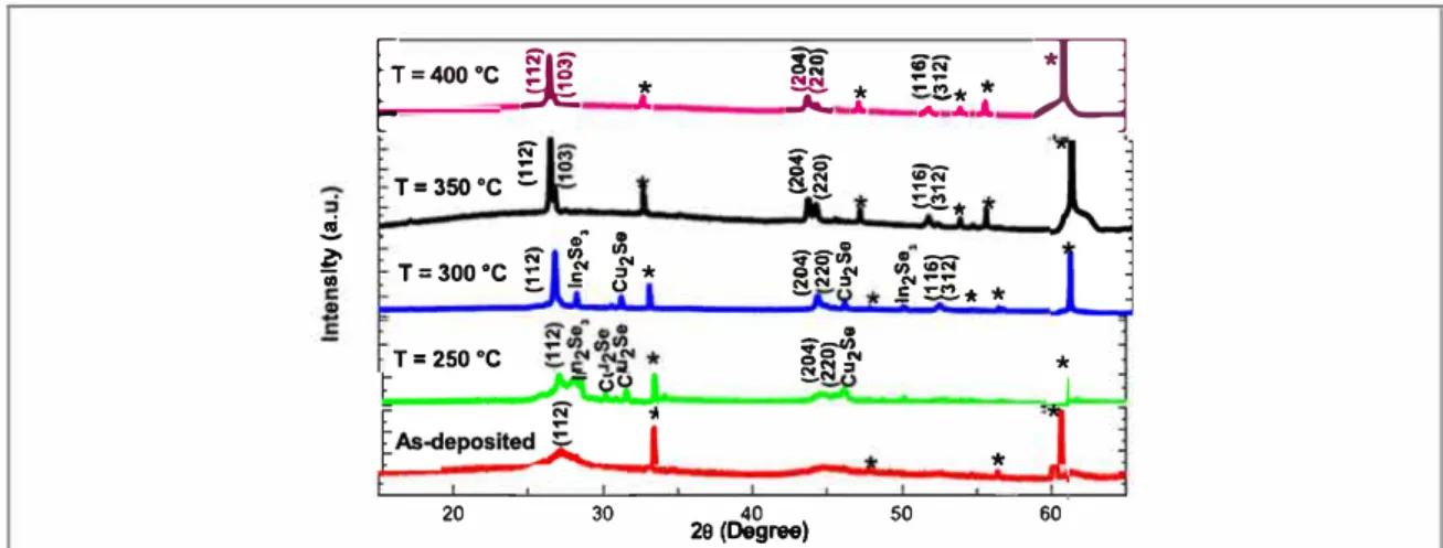
T•250 •c !:!.!:l" * * 20 30 28 (Degree) 40 50 60Figure 1. XRD patterns of electrodeposited CIS films on Si (100) substrate as a function of the annealing temperature. The peaks associated with Si (100) are highlighted by (*).
Table 1. Structural parameters of the as synthesized and annealed CIS films with RTP atvarious annealing temperatures.
Lattice constants (Â) Annealingtemperature T(°C) Bragg angle (°)
FWHM(0) Grain siu D (nm) a C $train (ë X 10 2)
As deposited 26.88 1.05 8.0 5.730 11.511 1.900
250 26.68 0.17 46.0 5.751 11.595 0.304
300 26.74 0.14 58.0 5.770 11.474 0.250
350 26.45 0.12 67.3 5.775 11.500 0.206
400 26.44 0.11 73.4 5.776 11.505 0.203
annealing of the as-deposited CIS films was carried out in a nitrogen atmosphere at temperature in the range of 250 -400 °Cfor 5 min byRTP using IRheating lamps.
2.2. Characterization
Structural characterization of the fabricated CIS thin films was done by XRD analysis in 20 mode ( 10° -70° angle range) using an automated Bruker D8 advanced diffractometer and the CuK"' ( À = 1 .540 Â) radiation. The
reflectance spectra R( À) of the electrodeposited CIS films was measured at room temperature by a UV-visible NIR LAMBDA 950 spectrophotometer for wavelengths ranging between 350 and 2000 nm. Surface cross sectional morphologies of the samples were observed by a scanning electron microscope ( SEM) JEOL JSM -5910 , with an accelerating voltage of20 kV. In addition, their compositions were determined by EDS.
Heterojunction solar cells with an active area of about 0 .7 8 cm2 have been fabricated using conventional
photolithography technique. Back and grid front aluminum (A l) contacts were deposited by thermal
evaporation followed by an annealing step. J-Y characteristics were measured by a digital source meter ( Keithley Instruments Inc. , M odel 2400) in the dark and under AM 1 .5 ( 100 m W cm 2) illumination.
3. Results and discussion
3.1. Structural analysis
XRD patterns recorded for CIS thin films grown on Si (100) substrates under different RTP annealing
temperature of250 °C, 300 °C, 350 °C and 400 °C are depicted in figure 1. According to the width ofXRD peaks, one guess that the grains' size of the as-deposited CIS layers is verysmall, e.g. those layers are amorphous. Alow crystallization appears for CIS film treated at 250 °C. When we increase the annealing temperature, the peaks
corresponding to (112), (103), (204), (220), ( 116) and (312) plans of the well-identified CIS chalcopyrite phase (Reference JCPDS 40 -14 87) appear. In addition, secondary phases of Cu2Se and In2Se3 are observed for
annealing temperature of250 °C, but th ose binary phases are not detected above 300 °C. Severa! investigations [20, 21] have proved that the formation of CuinSe2 is produced from the reaction between Cu2Se and I n2Se3.
Upon heat treatment at 350 °C, a single chalcopyrite structure phase is obtained with a strong and preferential orientation along the ( 112) direction. Similar (112 ) peak has also been observed for CuinSe2 films synthesized on
found to decrease from 612 to 396 arc seconds with an increase in annealing temperature from 250°C to 400 °C. This indicates that the crystalline nature of the samples improves when the RTP annealing temperature rises. Improved crystallinity was verified through the change in grain sizes, which were estimated from the highest peak intensity by the Scherrer’s formula expressed as equation (1) [22,23].
D k
cos , 1
l
b q
= ( )
whereλ is the wavelength of CuKα line (λ = 1.540 Å), θ is the Bragg angle, ß is the values of the FWHM of the (112) peak and k is a constant usually taken equal to 0.9. The calculated values of the crystallite size are given in table1. The largest crystallites with mean grain diameters of 67 and 73 nm are obtained at 350°C and 400 °C, respectively. Improvement of the crystallization is observed when the annealing temperature reaches 350°C. In table1, one can also note a small shift of the(112) peak to lower angle for temperatures of 350 °C and 400°C. This can be due to a better relaxation of the strain related to the in-plane lattice mismatch (6.0%) between CIS(a = 5.78 Å) and Si (5.45 Å). The lattice constants for CIS films assuming tetragonal symmetry are calculated using the following formula:
d h k a l c 1 , 2 hkk 2 2 2 2 2 2 = + + ( )
where d(hkl)is the inter-plane spacing. The two lattice parameters a and c are given in table1. They range from
5.730 to 5.776 Å and 11.474 Å to 11.595 Å, respectively. These values are in good agreement with those indicated in the JCPDS referencefiles [24]. The micro-strain ε was evaluated using the following relation [25]:
4 tan . 3
e b
q
= ( )
It is known that the micro-strainε affects the optoelectronic properties of the films due to the distorted lattice. Values ofε decreases from 1.9% for as-deposited sample to 0.2% for sample annealed at 350 °C. This is attributed to the reduced level of defect and grain boundaries due to increased grain size. Hence, annealing temperature of 350°C appears necessary for the formation of films with good structural quality.
3.2. Morphological and compositional analysis
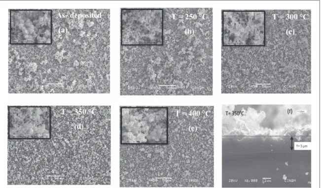
The surfaces morphologies of the electrodeposited CIS displayed infigure2were investigated by SEM. The latter shows that the annealing temperature affects the morphology of thefilms by changing the particles size. In fact, micrograph offigure2(a) shows non-homogeneous surface composed of grains with non-uniform distribution. When the annealing temperature reaches 350°C (figure2(d)), we notice a reduction of the size of the clusters leading to a homogenous surface. The grain’ size distribution appears to be relatively uniform with a mean crystallite size varying between 100 and 400 nm. Grains seen under SEM may contain several individual nanocrystals(NCs). This could explain the difference in values of crystallite size calculated from XRD data (about 70 nm) and those deduced from SEM micrographs. Otherwise, for the film treated at 400 °C, much larger grains appear while the surface morphology is more disordered(figure2(e)).
Figure2(f) provides a typical cross-sectional SEM image of the CIS film grown on Si (100) after annealing at 350°C. The deduced film thickness is around 3 μm, the layer looks dense, but the surface profile reveals a strong micrometer scale roughness. Such roughness is incompatible with imaging by atomic force microscopy leading to overestimated root mean squared roughness(rms) of 0.79 μm for the as-deposited sample. The surface profiles have been studied using a DEKTAK-XT profilmeter over scan length of 300 μm with a stylus force of 1 mg and a scan speed of 10μm s 1. The radius of curvature of the tip is 2μm. The rms were found to be 0.83μm for the as-deposited sample and 0.70 μm, 0.64 μm, 1.10 μm and 1.06 μm for samples annealed at 250°C, 300 °C, 350 °C and 400 °C, respectively. Those values agree with SEM morphologies observed in insert offigures2(a)–(e).
Table 2. The elemental composition of EDS patterns of CIS thin films at different annealing temperature.
Atomic ratio(%) Annealing temperature T(°C) Cu In Se 250 21.92 13.81 64.26 300 29.41 17.47 53.11 350 26.14 22.83 51.03 400 28.42 23.33 48.25
Figure3shows a typical EDS spectrum for sample annealed at 350°C that reveals the presence of copper, indium and selenium elements. Silicon is likely attributed to the substrate. Other elements such as residual oxygen and carbon may be due to surface and interface contaminations. The compositional analysis of those CIS films is summarized in table2. We note that the best stoichiometry in at% is obtained for CISfilm annealed at
Figure 2. SEM images of top surface and cross section of electrodeposited CIS layers on Si(100) before and after annealing using RTP furnace:(a) before annealing; (b) (e) annealed at 250 °C, 300 °C, 350 °C and 400 °C, respectively; (f) SEM cross section of simple annealed at 350°C.
200---N
-175 150 ':-� 125 � %-100 � � 75 50 25 • T = 250 °C •T
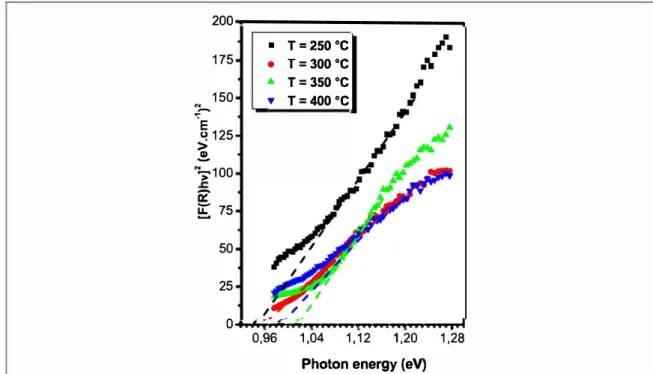
= 300 °C .t. T = 350 °C • T=400°C o ......... _... 0,96 1,04 1,12 1,20 1,28Photon energy (eV)
Figure 4. Plot of (F(R) hv)2 versus ( hv) using a Kubelka Munk approximation for CIS films deposited on si li con substrate at different
annealing ternperatures.
350 °C with no loss in Selenium. From the above results obtained by XRD, SEM and EDS analysis, it appears that samples annealed at 350 °C have improved crystallization properties.
3.3. Optical properties
The optical band gaps oflayers annealed at 250 °C, 300 °C, 350 °C and 400 °C were estimated in or der to determine which one presents the absorption edge closest to that of stoichiometric CIS semiconductor. Severa! investigations [26, 27) have reported methods to determine the absorption coefficient of electrochemically or -vacuum deposited thin films on non-absorbing substrates from measurements oflight reflectance. But in this case, it is difficult to evaluate the absorption coefficient of these films using the Lambert-Beer law. Hence, the total reflection spectra (specular and diffusion) were recorded using an integrated sphere on different spots for each film to minimize the error of missing the diffused component of the reflected beam. Besides, it is well known that CIS is a direct band gap semiconductor which can be estimated from the linear absorption coefficient, a, according to Tauc's formula [28):
ahv = A0 (hv -Eg)112, (4)
where hv is the incident photon energy, A0 is a constant and h is the Planck constant.
The absorption coefficient could be approximated using the Kubelka-Munkfunction F(R), defined with respect to reflectivity of dense samples (R
=
Roc) through the following equation:F(R) = (1 - R)2_
2R (5)
The optical band gap of CIS films has been calculated by plotting [ F(R) hv ]2 versus hv as illustrated in figure 4, where we extrapolate the straight line- portion of the absorption edge to find the intercept with energy axis. W e found that the band gap energyvalue increases from 0. 94 to 1.01 eV when the annealing tem perature rises. We also note that the sample annealed at 350 °Chave larger band gap (1.01 eV) than that one annealedat 400 °C (0.98 eV). In general, higher values of the optical band gaps are assigned to less intrinsic and extrinsic defects which give less contribution below the absorption edge. Similar result was shown by other studies [29,30). An optimum value ofEg
~
1.01 eVis likely with the formation ofasingle ternaryCIS phase.3.4. Optical modeling
A fitting pro gram written in Mathlab was used in order to extract the optical parameters such as the refractive index, n (À), the extinction coefficient k( À) and the band gap energy from experimental curves of reflectivity R
(À). We used the Fresnel matrix method applied to CIS thin films wherewe consider two consecutive layers in
contactwith air, e.g. an air/CuinSe2/ Si(l00)/ air stacking. Both layers have complex refractive indexes and
g
CIi u C u 0,09 0 0,08 0,07 0,06 0,05 0,04 Exprimental (R""") Theoretical (Rlh00) Instrumental noiseI
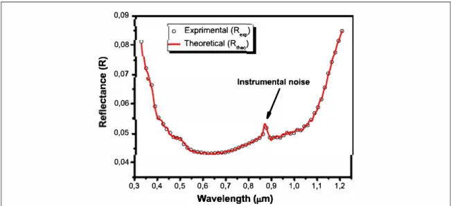
0,3 0,4 0,5 0,6 0,7 0,8 0,9 1,0 1,1 1,2 Wavelength (µm)Figure 5. Fitting results of theoretical Ru,..,( À) and experimental R,xp(À) reflectance spectra of CIS film after RTP annealing at 350 °C.
The instrumental noise is d ue to an automaticchange of detectors in the UV vis NIR spectrophotometer apparatus.
2,28--- 2,3x10⁴ ..---. 2,24 � 2,20 "C C � 2,16
:g
a, 2, 12 2,08 2,04*
�T=350°C*
(a)
*
*
*
*
*
*
0,2 0,4 0,6 0,8 1,0 1,2 Wavelength (µm)fil
2,2x10⁴·u
�8
C 0U
C 2, 1x10⁴ 2,0x10⁴ �-T=350°C (b) 0,2 0,4 0,6 0,8 1,0 1,2 Wavelength (µm)Figure 6. Optical parameters: (a) refractive index, n, and (b) extinction coefficient, k, versus wavelength for CuinSei thin films treated at350 °C.
on calculation methods using Fresnel matrixwithin this model are reported in our previous work [12). The theoretical values of optical parameters were determined using the Cauchy model according to the following equations:
B
C
n=A
+
-
+
-,
>..2
>,.
4 D E Fk=-+-+-,
).. )..3 )..5 (6) (7)where À is thewavelength and A, B, C, D, E and Fare constants. By fitting theoretical curve ofR(>.) to
experimental one over the entire spectral range [300--1300 nm] as plotted in figure 5, we can determine the band gap energy, the refractive index, n, and the extinction coefficient,
k,
of all films. Thereby, the best fitting result was obtained for theCrS
film after RTP annealing at 350°C.
Figures 6( a) and (b) show the variation in extinction coefficient and refractive index as a function of the
wavelength for
ers
film treated at 350°C,
which reveals a decreasing in refractive index and extinctioncoefficientwith increasingwavelength. Values of n and k reach 2.03 and 2.0 10 4, respectively, in the near infrared range.
2,06 2,1ax10• 2,16x10" 2,05 2,14x10" )(
=
..
2,12x10•a
.5..
2,04 2,1ox10• n1
Refractive index (n) Extinction coefficient (k) 2,08x10" 2,03 2,06x10"a
e 2,04x10" 2,02 2,02x10" 250 300 350 400 Annealing temperature (°C))Figure 7. Variation of the refractive index and the extinction coefficient of CIS films as a function of annealing temperature at set
wavelength À 1100 nrn.
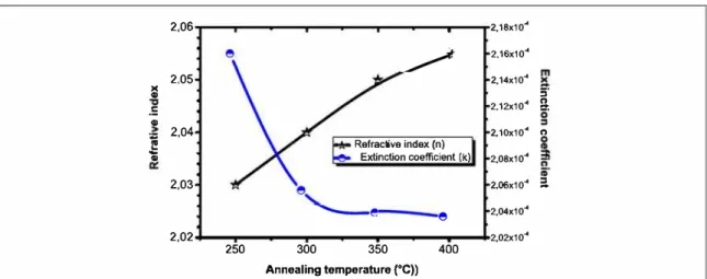
The effect of annealing temperature on the optical constants of CIS films are illustrated in figure 7 for a fixed wavelength of 1100 nm. The refractive index rises when the annealing temperature increases to a value of2.055 for films heated at 400 °C. This could be explained by a densification of the films after annealing. In contrast, the extinction coefficient decreases considerably with annealing temperature, reaching a value of about 2.04 x 10 4
for film annealed in the 350 °C-400 °C range. These results indicate the formation of a single CIS chalcopyrite phase ab ove 350 °C. The band gap energy was estimated from the absorption coefficient according to the following equation:
41r k
a:=-- (8)
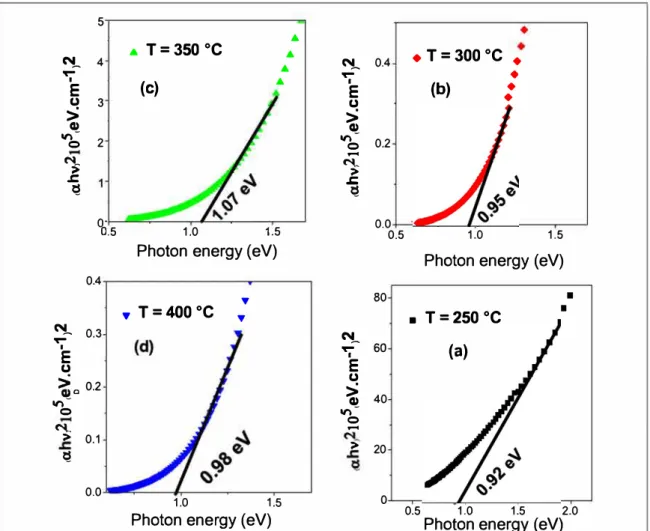
Values of the optical band gap Egof CIS layers as a function of annealing temperature are shown in figure 8.
The samples exhibit a gradual shift in the optical spectra towards higher energies. These band gaps range from 0.92 to 1.07 eV when the annealing temperature ris es. Thesevalues are in good agreement with those deduced
from the reflection spectra. The lower values ofEgobtained at 250 °C and 300 °C could be due to absorption by
impurity or by the In2Se3 secondary phase.
3.5. Current density-voltage characteriza tion
Highly polycrystalline CIS thin films were obtained using one-step electrodeposition upon galvanostatic mode on silicon substrate followed by RTP annealing at 350 °C. For front grid and back contacts, we thermally evaporate aluminum. The typical J-V characteristics of the fabricated Al/CIS /Si ( 100) heterojunction under dark and AMl .5 illumination are plot in figure 9. One can notice the rectifying behavior of this heterojunction under dark. Values of serial R. and shunt Rsh resistances are 2 n and 1000 n, respectively. Thesevalues arevery
interesting for such heterojunction solar cell. They indicatelow recombination (R.) and low leakage current (R.b). The cell exhibits a short circuit current density lsc of 4.06 mA cm 2, an open circuit voltage
V
oc of0.28 V, a fill factor FF of36.72% and a power conversion efficiency1] of0.41 %.V
oc and lsc are m uch lower than the ones o btained for solar cells fabricated by others cost-effectivetechniques in [31, 32). However, similar poor efficiencyof0.3% was obtained by Jin etal [33]with
heterojunctions based on CuinSe2 NCs/CdS quantum dots (QDs)/ZnO nanowire (NW) arrays. It is generally assumed that low FF are related to charge percolation in nanostructured materials such as CIGS, NCs, NWs or QDs. The low lsc may arise from a strong recombination of the photo-carriers at surface and interface states.
The low
V
oc value is surprising. It could be due to a corn posi tional band gap narrowing of CIS layer at the interface or to a type II CIS/Si tunneling interface.Further works could improve the cell performances through (i) optimizing the physicochemical surface preparation of the silicon substrate, (ii) a mechanical chemical polishing of CIS layers, (iii) a surface passivation of CIS nanocrystallites, (iv) the use of a transparent conductive oxide deposited in a conformal way by atomic layer deposition, or (v) through the incorporation of Ga into the absorber to increase the band gap energy. For that purpose, an accurate study of the chemical bonding should be done by x-ray photoemission spectroscopy at each step of process.
5 À
•
T = 350 °C
À ♦T = 300 °C
� 4 À N_ 0.4•
"'""
1"'""
•
(c)
À 1(b)
E E•
C, 3 C,•
>
�>
�.,..
0 2.,..
0-
0.2 M,._ > M,._ >.c
.c
I;! I;! °ci.5 1.0 1.5 0.0 0.5 1.0 1.5Photon energy (eV)
Photon energy (eV)
0.4
"'
80 ■•
T=400 °C
"'
■T = 250 °C
■ N_ 0.3 �"'""
1"'""
60(a)
E 1 C, E �0 0.2 C,>
40.,..
� 0.,..
0 M,._ -> 0.1 > 20 I;! 0.0 0 1.0 1.5Photon energy (eV)
0.5Photon energy (eV)
1.0 1.5 2.0Figure 8. Plots of (o.hv)2 versus photon energy (hv) using optical modeling for CIS films on silicon substrate at various annealing
ternperatures.
o:i,
o.
-0,5 0,0 0,5 1,0 + + 0,0 ■ ... J. -oark -0,2 �t
T
T
+ -0,41
1 1N-f
+ E -0,6 u\
,
t-0,8 .?;,-1,0 ëii C: 5 � ....,llght 0 'E .5\_
t
� V 0c = 0.28 V....
::, -10 (.) J 5c= 4.06 mA/cm21
-15-
t--20 FF = 36.72 % -25 Tl= 0.41 %�
J
_, -30-1,0 -0,5 0,0 0,5 1,0 Volatge (V)4. Conclusion
In summary, a galvanostatic electrodeposition method was successfully employed to deposit CulnSe2 thin films
on monocrystalline Si (100) substrates. The as-deposited films are amorphous thus requiring RTP heat treatment. The effect of annealing temperature on physicochemical proprieties of CIS films was investigated by XRD, SEM and EDS analysis. We pointed out the formation at 350 °C of nanocrystalline layers of single phase stoichiometric CIS with preferential orientation along (112) direction.
The optical modeling showed that the refractive index and the extinction coefficient in the near infrared region (À
=
1100 nm) are greatly influenced by the annealing temperature. The optical band gap measured byUV-visible-IR reflectance is about 1.01 eV which is close to that calculated by optical modeling of theoretical spectra (1.07 eV).
The electrical characteristics of CIS / c-Si based heterojunction solar cell were assessed by J-V measurements
under dark and AM 1.5 illumination. A 36.72% fill factor, a 4.06 mA cm 2 short circuit current density, a 0.28 V
open circuit voltage, and a O .41 % power conversion efficiency were obtained These poor performances may be explained bypercolation of the photo-carriers to the Al contact surface and to CIS / Si interface followed by a strong recombination at defect states. Capacitance-voltage spectroscopy may help to understand the origin of
the low value of Yoc• The minority carrier lifetime should be adressed as well.
Nevertheless, this novel one step electrodeposition approach has proved being successful to fabricate a
heterojunction cell between a nanocrystalline CulnSe2 film and amonocrystalline silicon substrate. Although
perfectible, this simple process allows an easy control of the chemical composition of CIS layers, and could be applicable to produce CIS based solar cell and modules.
Acknowled
gments
Authors would like to thank Vasile Heresanu, Damien Chaudanson, Alain Ranguis and Frédéric Bedu from the Centre Interdisciplinaire de Nanoscience de Marseille for their fruitful help in characterization of CIS samples by XRD, SEM, EDS, AFM and surface profilometry, respectively.
ORCIDiDs
M Bouaïcha G https:ff orcidorg/0000-0002-6294-2541
References
(1) Compaan AD 2006 Photovoltaics: clean power for the 21st centurySol. Energy Mater. Sol. Cells90 2170 80
(2) TéllezH, Druce J, Hall A, Ishihara T, Kilner J and Rockett A2015 Lowenergy ion scattering: surface preparation and analysis of Cu(In,Ga)Sei for photovoltaicapplications Prog. Photovolt Res. Appl. 23 1219 27
(3) Jackson P, Hariskos D, Lotter E, Paetel S, WuerzRand Menner R201 l Polycrystalline Cu(InGa)Sei/CdS thin filmsolar cells madeby newprecursors Prog. Photovolt., Res. Appl. 19 894 7
(4) Maeda T, Takeichi T and Wada T2006 Systematic studies on electronicstructures of CulnSei and the other chalcopyrite related compounds byfirst principles calculations Phys. Status Solidi a 203 2634 8
(5) DuchateletA, Sidali T, Loones N, SavidandG, ChassaingE and Lincot D 2013 12.4% Efficient Cu (In,Ga)Sei solar cell prepared from one step electrodeposited Cu In Ga ox:ide precursor layer SoL Energy Mater. SoL Cells 119 241 5
(6) Contreras MA, RomeroM J and Noufi R 2006 Characterization of Cu( ln,Ga)Sei materials used in record performance solar œlls Thin
Solid Films 51 511 2
(7) Krunks M, IGjatkina 0, Rebane H, Oja I, Mikli V and Mere A 2002 Composition of CulnS;i thin films prepared by spray pyrolysis Thin Solid Films 403 40 4 71 5
(8) Mustfa H, Hunter D, Pradhan A K, RoyU N, Cui Y and Burger A 2007 Synthesis and characterization of Agln$ei for application in thin film solar cells Thin Solid Films 515 7001 4
(9) Wellings J S,SamantillekeA P, HeavensSN, Warren P and Dharmadasa l M 2009 ElectrodepositionofCulnSe.i from ethyleneglycol at 150 °CSoL EnergyMater.SoL Ce11s93 1518 23
(10) Mandati S,SaraclaB V, Dey S R and Joshi SV 2013 Pulsed electrodepositionof CulnSe.i thin films with morphology forsolarcell applications/. Electrochem. Soc. 160 173 7
(11) Meglali 0, AttafN, Bouraiou A, Bougdira J, Aida M S andMedjahdi G 2014 Chemicalbath composition effect on the properties of electrodeposited Culn$ei thin films J. Alloys Compd. 587 303 7
(12) Saidi H, BoujmilM F, Durand B andBouàicha M2017 Physical properties of highly crystallineCIS layer prepared usingsingle phase electrodeposition and low temperature RTP annealing J. Alloys Compd. 695 779 86
(13) Taunier S eta/2005 Cu(In,Ga)( S,Se)i solar cells and modules byelectrodeposition Thin SolidFilms 480 481 526 31 (14) Kessler F and Rudmann D 2004 Technological aspects offlexibleCIGS solarcells and modules Sol. Energy77685 95
(15) Otte K, Makhova L, Braun A and Konovalov I 2006 FlexibleCu(In,Ga)Sei thin filmsolar cells for spaœ application Thin SolidFilms
511 512613 22
(16) Ivanou D K,StreltsovEA, Fedotov A K, MazanikA V, FinkD and Petrov A 2005 Electrochernical deposition of PbSe andCdTe nanopartides onto p Si (100) wafers and into nanopores in SiO2/ Si(l 00) structure Thin Solid Films 490 154 60
[18] Tiwari A N, Blunier S, Filzmoser M, Zogg H, Schmid D and Schock H W 1994 Characterization of heteroepitaxial CuIn3Se5and
CuInSe2layers on Si substrates Appl. Phys. Lett.65 3347
[19] Aissaoui O, Mehdaoui S, Bechiri L, Benabdeslem M, Benslim N, Amara A, Mahdjoubi L and Nouet G 2007 Synthesis and material properties of Cu III VI2chalcopyrite thinfilms J. Phys. D: Appl. Phys.40 5663 5
[20] Deng W, Yan Z, Ding P, Wang Y, Fang Y, Su M and Su Y 2014 Phase composition of CuInSe2in different annealing process Mater. Sci.
Semicond. Process.26 419 24
[21] Papadimitriou D, Roupaka G, Sáez Araoz R, Lux Steiner M C, Nickel N H, Alamé S, Vogt P and Kneissl M 2015 Quality CuInSe2and
Cu(In,Ga)Se2thinfilms processed by single step electrochemical deposition techniques Mater. Res. Express2 056402
[22] Faraday M 1834 Experimental researches in electricity. Seventh series Phil. Trans. R. Soc.124 77
[23] Weast R C (ed) 1980 CRC Handbook of Chemistry and Physics (Boca Raton, FL: CRC Press)
[24] Fons P, Niki S, Yamada A, Uchino M and Oyanagi H 2000 Copyright © JCPDS International Centre for Diffraction Data, Advances in X ray Analysis 43, 201 11
[25] Vanheusden K, Seager C H, Warren W L, Allant T D R and Voigt J A 1996 Correlation between photoluminescence and oxygen vacancies in ZnO phosphors J. Appl. Phys. Lett.68 403 5
[26] Zarpellon J, Jurca H F, Klein J J, Schreiner W H, Mattoso N and Mosca D H 2002 Electrodeposition of Fe thin films on Si (111) surfaces in the presence of sodium saccharin Electrochim. Acta53 2002 8
[27] Tuttle J R, Albin D S, Matson R J and Noufi R 1989 A comprehensive study on the optical properties of thin film CulnSe2as a function of
composition and substrate temperature J. Appl. Phys.66 4408 17
[28] Guillén C and Herrero J 1991 Optical properties of electrochemically deposited CulnSe2thinfilms Sol. Energy Mater.23 31 452
[29] Zouaghi M C, Nasrallah T B, Marsillac S, Bernèd J C and Said B 2001 Physicochemical characterization of spray deposited CuInS2thin
films Thin Solid Films 39 46 382
[30] Koutsikou R and Bouroushian M 2015 Pulse potential electrodeposition of (112) textured chalcopyrite CuInSe2films from acidic
aqueous solutions Electrochim. Acta178 856 70
[31] Pathak D, Bedi R K and Kaur D 2010 Growth of heteroepitaxial AgInSe2layers on Si(100) substrates by hot wall method Optoelectron.
Adv. Mater. 4 657 61
[32] Liu W, Mitzi D B, Yuan M, Kellock A J, Chey S J and Gunawan O 2010 12% efficiency CuIn(Se,S)2photovoltaic device prepared using a
hydrazine solution process Chem. Mater.22 1010 4
[33] Guo Q J, Kim S J, Kar M, Shafarman W N, Birkmire R W, Stach E A, Agrawal R and Hillhouse H W 2008 Development of CuInSe2