HAL Id: hal-00733538
https://hal.archives-ouvertes.fr/hal-00733538v4
Submitted on 20 Aug 2014HAL is a multi-disciplinary open access archive for the deposit and dissemination of sci-entific research documents, whether they are pub-lished or not. The documents may come from teaching and research institutions in France or abroad, or from public or private research centers.
L’archive ouverte pluridisciplinaire HAL, est destinée au dépôt et à la diffusion de documents scientifiques de niveau recherche, publiés ou non, émanant des établissements d’enseignement et de recherche français ou étrangers, des laboratoires publics ou privés.
statistical modeling of the sensor raw data
Cecilia Aguerrebere, Julie Delon, Yann Gousseau, Pablo Musé
To cite this version:
Cecilia Aguerrebere, Julie Delon, Yann Gousseau, Pablo Musé. Study of the digital camera acquisition process and statistical modeling of the sensor raw data. 2013. �hal-00733538v4�
statistical modeling of the sensor raw data
C. Aguerrebere, J. Delon, Y. Gousseau, P. Mus´e
1
Introduction
The accurate modeling of the acquisition process in digital cameras is of great interest for a wide variety of domains concerning the use of digital images. In particular, it is of great utility in image processing, computational photography or computer vision applications. For instance, the statistical characterization of image data allows to develop denoising techniques suited to particular noise types, which perform much better than general tech-niques.
In the present report we present a detailed analysis of the digital image acquisition process which allows us to introduce a statistical model of the raw sensor data. The accuracy of this modeling is essential to its posterior utility. It is thus fundamental to take into account all different sources of noise and uncertainty in this model.
Several articles present and make use of statistical models of the sensor raw data (Tsin et al., 2001; Robertson et al., 2003; Kirk and Andersen, 2006; Granados et al., 2010; Foi et al., 2008). Different levels of complexity can be found among them. In particular, a model similar to the one presented in this work can be found in (Kirk and Andersen, 2006; Granados et al., 2010; Foi et al., 2008). Nevertheless, to the best of our knowledge, non of these articles present a detailed explanation of the physical origin of each noise source and the corresponding justification of the statistical model associated to each one. This rigorous analysis enables us to prioritize the different noise sources and obtain a simplified model still useful and realistic. Also we are able to consciously determine other aspects of the model, for instance, the relevance of considering spatially varying parameters.
2
Acquisition of digital images
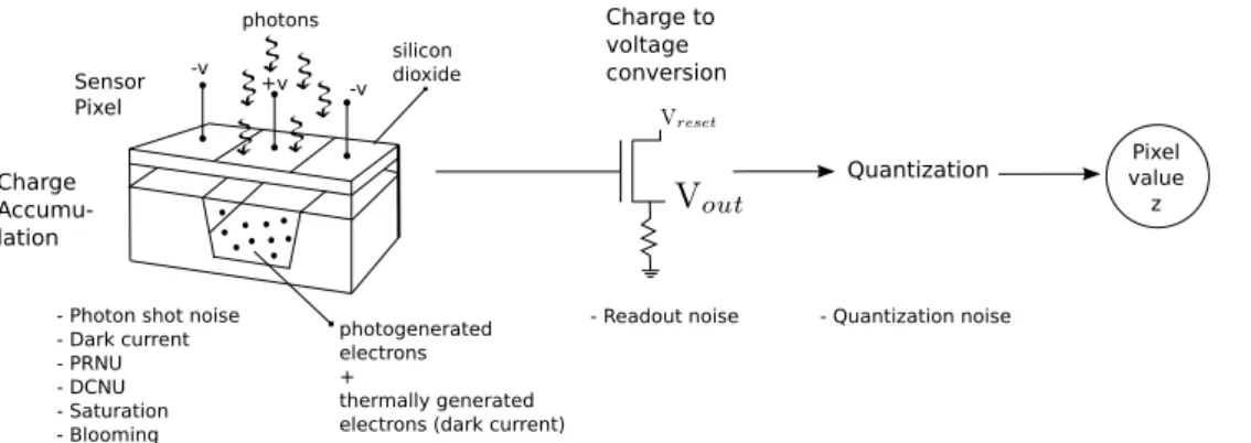
Two technologies are used for camera sensors: charge-coupled devices (CCD) and com-plementary metal–oxide–semiconductors (CMOS). Even if the operation principles of both sensors differ, a very similar acquisition model can be proposed for both of them, illustrated by a simplified diagram in Figure 1. In short, CCDs and CMOS both transform incoming light photons into voltage output values. More precisely, these sensors are silicon-based
Charge Accumu-lation
- Photon shot noise - Dark current - PRNU - DCNU - Saturation - Blooming - Readout noise photogenerated electrons + thermally generated electrons (dark current)
silicon dioxide Charge to voltage conversion - Quantization noise Sensor Pixel photons +v -v -v Pixel value z Quantization
Figure 1: Simplified diagram of the main stages of the acquisition process and the principal noise sources at each stage.
integrated circuits including a dense matrix of photo-diodes that first convert light pho-tons into electronic charge (Theuwissen, 1996; Brouk et al., 2008). Light phopho-tons interact with the silicon atoms generating electrons that are stored in a potential well. When the potential well is full, the pixel saturates, and no further electrons are stored 1. In the case
of CCDs, the accumulated charge may then be efficiently transferred from one potential well to another across the chip, until reaching an output amplifier where the charge is con-verted to a voltage output value. This voltage is then quantified to give the corresponding pixel value. For the CMOS technology, the impinging photons are also accumulated in the photo-diodes. However, unlike CCDs, CMOS pixels have conversion electronics to perform the charge to voltage conversion at each location. This extra circuitry increases noise and generates extra fixed pattern noise sources compared to CCDs (Brouk et al., 2008). The main uncertainty sources at each stage of the acquisition process are described in more details in the following paragraphs, and listed by Figure 1. We divide them in two categories: random noise sources, and spatial non-uniformity sources.
2.1
Random noise sources
Two physical phenomena are responsible for the random noise generation during the camera acquisition process: the discrete nature of light, which is behind the photon shot noise, and thermal agitation, which explains the random generation of electrons inside the sensor when the temperature increases.
2.1.1 Photon shot noise
The number of photons Cpi impinging the photo-diode p during a given exposure time τi
follows a Poisson distribution, with expected value Cpτi, where Cp is the radiance level
1In this case, additionally generated electrons may spill over the adjacent wells, resulting in what is
called blooming. This phenomena, well known in astronomic photography, is mostly observed with very long exposures. We neglect it in this paper.
in photons/unit-of-time reaching the photo-diode. If we suppose that an electron is gen-erated for each absorbed photon (this depends on the photon energy, therefore on the considered wavelength), the number of electrons generated on the potential well is also Poisson distributed. In an ideal case with no other noise sources, the voltage measured at the sensor output should be proportional to the collected charge: V = gcvCpτi, where
Cpτi is the number of absorbed electrons, and where gcv is the equivalent capacitance of
the photo-diode.
2.1.2 Dark current
Some of the electrons accumulated on the potential well don’t come from the photo-diode but result from thermal generation. These electrons are known as dark current, since they are present and will be sensed even in the absence of light. Dark currents can be generated at different locations in the sensor and they are related to irregularities in the fundamental crystal structure of the silicon, e.g. metal impurities (gold, copper, iron, nickel, cobalt) and crystal defects (silicon interstitials, oxygen precipitates, stacking faults, dislocations) (Theuwissen, 1996). For an electron to contribute to the dark current it must be thermally generated but also manage to reach the potential well. This last event happens independently for each electron. As a consequence, it can be shown that the number of electrons Dp thermally generated and reaching the potential well p is well modeled by a Poisson distribution with expected value Dp (Theuwissen, 1996), depending
on the temperature and exposure time. This noise is generally referred to as dark current shot noise or dark shot noise. In this paper, in order to make explicit the dependence on the exposure time τi, we name this dark shot noise Dpi.
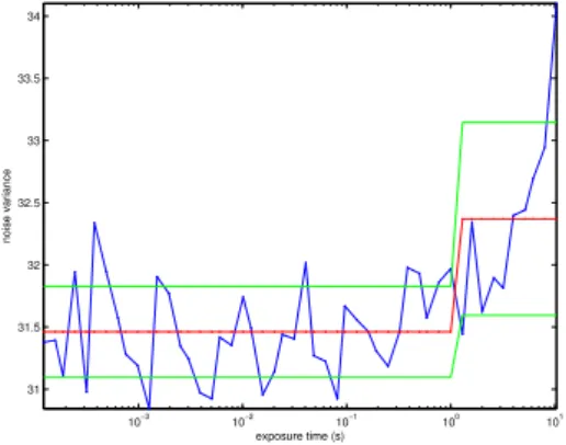
It has been stated that dark currents can be neglected for exposure times under 1 sec-ond (Martinec, b). The following experiment was csec-onducted to verify this result for the Canon 7D camera. Dark frames (frames acquired in a dark room with a camera without lens and with the cap on) were acquired for exposure times in the range 1/8000 to 10 sec-onds and ISO set to 100. The noise variance for each frame was computed as the variance from all pixels. This variance includes the readout noise variance and the dark current shot noise variance. Figure 2 shows the obtained results. The noise variance is nearly constant up to 1 second and then increases with the exposure time for exposures above 1 second. The dark current expected value increases with the exposure time. Since this behavior is not observed for the variance values between 1/8000 and 1 second, we conclude that the dark current variance is masked by the readout constant variance and is therefore negligible with respect to it for exposure times below 1 second.
2.1.3 Readout noise
In the readout stage of the acquisition process a voltage value is read for each pixel. This voltage is read as a potential difference from a reference level which represents the absence of light. Thermal noise Nreset, inherent to the readout circuitry, affects the output values.
10−3 10−2 10−1 100 101 31 31.5 32 32.5 33 33.5 34 exposure time (s) noise variance
Figure 2: Noise variance vs. exposure time for dark frames (blue). The red ”step” shows the mean noise variance for the exposures below 1 second and then for those above 1 second. The band delimited by the green lines represents one standard deviation from the mean value. Notice that the noise increases for exposures above 1 second.
distributed (Mancini, 2002). It is also known as reset noise, in reference to the reference voltage, commonly named reset voltage.
Notice that modeling the noise source as Gaussian distributed means that pixels may take negative values. In practice, the reference voltage is assigned a large enough value in the AD conversion so that voltage values below the reference are assigned positive pixel values. For this reason, the raw data for an image taken with the cap on will give pixel values close to the offset value (e.g. 2048 for the 14 bits Canon 7D). Alike the raw pixels, the inverse of the camera response function f−1(z) may take negative values. Mostly for low radiance,
after subtracting the offset the inverse of the camera response may take negative values. The readout noise Nout includes also the remaining circuitry noise sources between the
photoreceptor and the AD circuitry. They are all thermally generated and thus modeled as Gaussian noise. Some other minor sources include frequency dependent noise (flicker noise) but we wont consider them in this analysis.
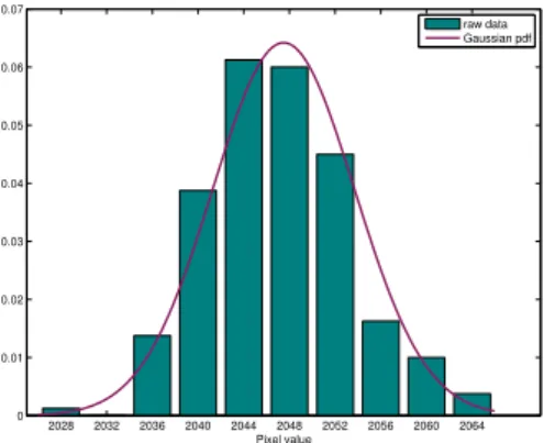
Figure 3 shows the histogram of the raw values taken by 200 realizations of one pixel. These realizations are obtained from 200 bias frames (images acquired with virtually no light, i.e, in a dark room with a camera without lens and with the cap on using the shortest possible exposure) acquired with a Canon 7D camera set to its shortest exposure (1/8192.0 s). The camera acquires virtually no light, thus the pixel value captures the readout noise in that pixel (the dark current can be neglected as shown in the previous experiment). The Gaussian probability density function, with mean and variance computed from the raw data, is superposed for comparison. The Gaussian distribution accurately approximates the readout noise distribution. Moreover, this experience shows the presence of the offset value previously mentioned. Even if the images are acquired with no light, the mean pixel value is not zero but 2048.
2028 2032 2036 2040 2044 2048 2052 2056 2060 2064 0 0.01 0.02 0.03 0.04 0.05 0.06 0.07 Pixel value raw data Gaussian pdf
Figure 3: Readout noise. Green: histogram of the raw values taken by 200 realizations of one pixel acquired with virtually no light (realizations are obtained from 200 bias frames acquired with a Canon 7D camera set to its shortest exposure 1/8192.0 s). Violet: Gaussian probability density function with mean and variance computed from the raw data. The distribution of the raw pixels is accurately approximated by a Gaussian distribution.
2.2
Spatial non-uniformity sources
Besides random noise sources, several uncertainty factors, all related to the spatial non-uniformity of the sensor, should be taken into account in the acquisition model.
2.2.1 Fixed pattern noise sources
Photo-response non-uniformity (prnu) The prnu describes the differences in pixel responses to uniform light sources. Different pixels wont produce the same number of elec-trons from the same number of impacting photons. We assume one electron is generated per absorbed photon, but not all the impinging photons will be absorbed in the photo-diode. This is caused by variations in pixel geometry, substrate material and micro-lenses (Irie et al., 2008). The effect of prnu is proportional to illumination and is prominent under high illumination levels. This noise source is signal dependent since there is no prnu in the absence of signal.
The fact that a photon can be absorbed or not in the photo-diode is a binomial selec-tion of the Poisson process of impinging photons. Hence the prnu can be modeled as a multiplicative factor ap applied to the parameter of the Poisson variable Cpi.
Dark-current non-uniformity (dcnu) The dcnu represents the variations in dark current generation rates from pixel to pixel. This variation is intrinsic to the material characteristics of the sensor cells and causes variations in the expected value of the dark current from pixel to pixel. As the prnu, the dcnu can be modeled as a multiplicative factor dp applied to the parameter of the Poisson variable Dpi.
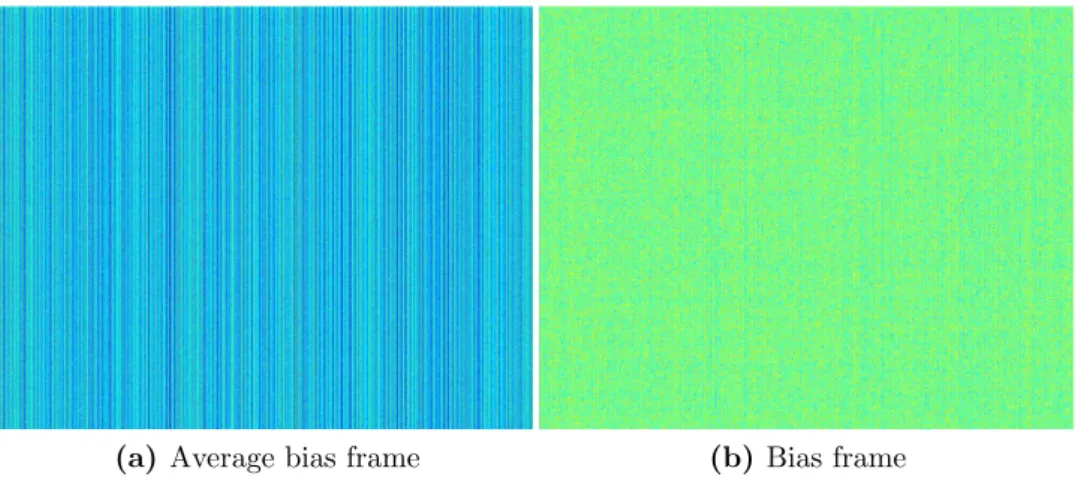
(a) Average bias frame (b) Bias frame
Figure 4: Column noise. Left: Average of 200 bias frames acquired with a CMOS sensor. Right: Bias frame acquired with a CMOS sensor.
Signal Dependent Temperature Dependent Exp. Time Dependent Photon shot noise Thermal noise Photon shot noise
prnu Dark current Dark current shot noise Thermal noise Table 1
2.2.2 CCD specific sources
Transfer efficiency After charge is collected at each pixel, the CCD must transfer the charge to the output amplifier for readout. The transfer efficiency of a real CCD sensors is less than 1. Charge that is not correctly transferred is either lost or deferred to other transfers, affecting other pixels count values. Current buried-channel CCD transfer effi-ciency is above 0.99999 (Healey and Kondepudy, 1994) thus it wont be taken into account in the acquisition model.
2.2.3 CMOS specific sources
Column noise The readout for CMOS sensors is performed line by line. At a given time, all columns of one line are readout through the output column amplifiers. Differences from one column amplifier to another introduce a column fixed pattern. Because the human eye is adapted to perceive patterns, column noise may be quite disturbing even if its contribution to the total noise is less significant than that of white noise (Martinec, a). Figure 4a shows the average of 200 bias frames acquired with a CMOS sensor (Canon 7D set to exposure time 1/8192.0 s). The column pattern on the readout noise is clearly visible. Figure 4b shows an example of one bias frame. The column pattern is not so evident from just one frame, but a subtle column pattern is still noticeable.
ac-cording to their dependence on signal, temperature and exposure time. Table 1 shows a classifications of the different noise sources according to these aspects.
2.3
Quantization noise
A last source of noise in the acquisition process takes place during the conversion of the analog voltage measures into digital quantized values or data numbers (DN). When the signal variation is much larger than 1 DN 2, the quantization noise can be modeled as
additive and uniformly distributed. In that case, it is usually negligible compared to the readout noise (Healey and Kondepudy, 1994). This being even more remarkable for modern cameras, which can easily have 12 or 14 bits for quantization.
The following experiment was conducted to verify the previous statement. The variance of a bias frame gives the variance caused by the readout process including the quantization noise. Several tests were performed with a Canon 7D and a Canon 400D, acquiring bias frames with different ISO settings. The variance values obtained are: Canon 400D, ISO 100 var = 2.5, ISO 400 var = 6.3, ISO 800 var = 17.2. Similar values are found by Granados et al. (2010) for a Canon 5D set to ISO 400 (var = 6.5) and a Canon PowerShot S5 set to ISO 400 (var = 18). As previously stated, except in low light conditions, the quantization noise can be modeled as uniformly distributed with variance equal to 1/12. Hence, in all of the tested configurations, the contribution of the quantization noise to the total readout variance is negligible (in the worst case 2.5 compared to 1/12). Moreover, the variance of the quantization noise in the worst case scenario (regardless of the illumination level) is 1/4, the worst possible error being 1/2. Thus, the contribution of the quantization noise to the total readout variance can also be neglected in low light conditions for the tested configurations (1/4 compared to 2.5). However, the margin is not so large in that case and counterexamples are certainly possible.
Given the recent advances in digital images acquisition techniques, and the corresponding decrease on the readout noise values, it may be interesting to include the quantization noise effects in order to develop a more precise camera acquisition model.
It is known that even if the power of quantization noise is negligible with respect to the other noise sources, its structured nature (it is not white) may make it noticeable after non linear post-processing. Nevertheless, when considering a noise model for raw data only, i.e., before non linear post-processing, the hypothesis of negligible quantization noise, except in low light conditions, remains valid.
2.4
Acquisition model
Equation (1) proposes a simplified model including the previously presented noise sources (the dependence on position p is avoided to simplify the notation):
Zi = f ([gcv(Ci+ Di) + Nreset]gout+ Nout+ Q) , (1)
2This is the case for non low light conditions since under the Poisson model, the irradiance mean and
Figure 5: Camera response function for the lineal + saturation model.
where f is the camera response function, Zi is the raw pixel value, Ci is a Poisson variable
of parameter aCτi, Di is a Poisson variable of parameter dDi. In the case of RAW data, f
is a linear function of slope 1 before attaining a saturation threshold (see Figure 5). After this saturation threshold, values are clipped (f becomes a constant). Equation (1) can be rewritten as the addition of a Poisson distributed random variable with expected value λi = aCτi + dDi, a Gaussian distributed noise component NR = goutNreset + Nout with
mean µR and variance σ2R, and the uniformly distributed quantization error Q:
Zi = f (gPoiss(λi) + NR+ Q) , (2)
with g = gcvgout.
A similar model is presented by Foi et al. (2008), where they propose to model digital camera raw data as a mixed Gaussian-Poisson model. The difference between the models is the inclusion of the gain gcv, modeling charge to voltage conversion. This constant is
not included in Foi et al. model, but the general idea remains the same.
The previous model is valid for both CCD and CMOS sensors. In the CCD case, the readout noise sources can be considered as identical for all pixels. Thus g, µR and σ2R are
spatially constant. On the contrary, in order to model column noise for CMOS sensors, different g, µR and σR2 parameters should be considered for each column.
2.5
Simplified acquisition model
For the values usually taken by λi = aτiC + dDi, the Poisson distribution can be correctly
approximated by a Gaussian distribution with mean and variance equal to λi. Regarding
the relative importance of each noise source, under low illumination conditions the primary noise source is the reset noise, while for high illumination the major noise source is the photon shot noise (Healey and Kondepudy, 1994). The dark currents can be neglected for exposure times below 1 second (Martinec, b) and, except in low illumination conditions, the quantization noise can be neglected compared to the readout noise (Healey and Kondepudy, 1994). Thus the model (2) can be simplified into
f−1(Z
with σ2
Rthe variance of NR. In the following sections, we will always assume that the
cam-era response f is linear before saturation (recall that we work with RAW data). Including the slope of f into the gain g, for non saturated samples the model becomes
Zi ∼ N (gaC τi+ µR, g2aCτi+ σ2R). (4)
which leads a simple yet realistic representation of raw sensor data.
3
Camera calibration procedure
In this section we describe a camera calibration procedure for the estimation of the camera parameters. This procedure is based on the work by Granados et al. (2010).
Readout noise mean and variance The readout noise mean and variance are com-puted from a bias frame. According to Model (4), where the readout noise mean and variance do not depend on the pixel position, these can be obtained computing the empir-ical mean and variance from all the pixel values of the bias frame,
ˆ µR = 1 N N X j=1 bj σˆ2R= 1 N − 1 N X j=1 (bj − µR)2, (5)
where bj, j = 1, . . . , N are the pixel values of the bias frame.
This estimation neglects the variance of the dark current and the quantization noise with respect to that of the readout noise.
Gain In order to estimate the camera gain we first note that, from Model (4), the mean and variance of any pixel Z verify
µZ= gaτ C + µR (6) σ2Z= g2aτ C + σR2, (7) thus we have g = µZ− σ 2 R σ2 Z− µR . (8)
Flat fields (i.e., images captured illuminating the sensor with a spatially uniform, narrow band light source) are thus used to estimate the pixels mean and variance and compute the corresponding g value. The pixels mean is computed according to
ˆ µZ= 1 N N X j=1 zj, (9)
where zj, j = 1, . . . , N are the pixel values of a flat field. The pixels variance is computed
from the difference of two flat fields in order to compensate for the variance introduced by the prnu effect
ˆ σZ2 = 1 2(N − 1) N X j=1 (z1j − z2j) 2, (10) where z1
j and z2j are the corresponding pixels of the two flat fields. Finally we have,
ˆ g = 1 2(N −1) PN j=1(z1j − z2j)2− σR2 1 N PN j=1zj− µR . (11)
In practice, the creation of a flat field is not a trivial task and can highly complicate the calibration procedure. An alternative to this is to compute the gain factor from image sub-regions that correspond to flat regions. Instead of computing the gain factor from all image pixels, we use all the pixels in the image sub-regions that correspond to the same illumination level. This is possible since the gain factor is a global parameter (i.e. the same for all pixel values), and its value should remain the same either computed from the complete flat frame or from a corresponding sub-region. In order to have a more robust estimate, the average of several estimates from flat sub-regions should be considered.
Photo response non uniformity Flat fields can also be used to estimate the spatially varying factors of the photo response non uniformity. From Model (4) we have
µZj = gajτ C + µR, (12)
where Zj denotes the j-th pixel location of the flat field. The mean µZj can be estimated
from M flat fields as
ˆ µZj = 1 M M X m=1 zmj , (13) where zm
j denotes the j-th pixel location of the m-th flat field. Then the prnu factor at
location j can be estimated as
ˆ aj = ˆ µZj− µR 1 N PN h=1µˆZh− µR . (14)
Saturation threshold Most saturated samples are clearly identifiable since they are assigned the maximum output pixel value. However, some saturated samples may be assigned a slightly inferior value due to readout noise. For this reason, the saturation threshold should be set to a percentage (98% in our tests) of the maximum output pixel value.
References
Brouk, I., Nemirovsky, A., and Nemirovsky, Y. Analysis of noise in CMOS im-age sensor. In Proceedings of IEEE International Conference on Microwaves, Com-munications, Antennas and Electronic Systems (COMCAS), pages 1–8, 2008. doi: dx.doi.org/10.1109/COMCAS.2008.4562800.
Foi, A., Trimeche, M., Katkovnik, V., and Egiazarian, K. Practical Poissonian-Gaussian Noise Modeling and Fitting for Single-Image Raw-Data. IEEE Transactions on Image Processing, 17:1737–1754, 2008. doi: 10.1109/TIP.2008.2001399.
Granados, M., Ajdin, B., Wand, M., Theobalt, C., Seidel, H. P., and Lensch, H. P. A. Optimal HDR reconstruction with linear digital cameras. In Proceedings of IEEE Conference on Computer Vision and Pattern Recognition (CVPR), pages 215–222, 2010. doi: dx.doi.org/10.1109/CVPR.2010.5540208.
Healey, G. and Kondepudy, R. Radiometric CCD camera calibration and noise es-timation. IEEE Transactions on Pattern Analysis and Machine Intelligence, 16(3):267 –276, 1994. doi: dx.doi.org/10.1109/34.276126.
Irie, K., McKinnon, A. E., Unsworth, K., and Woodhead, I. M. A model for mea-surement of noise in CCD digital-video cameras. Meamea-surement Science and Technology, 19(4), 2008. doi: 10.1088/0957-0233/19/4/045207.
Kirk, K. and Andersen, H. J. Noise Characterization of Weighting Schemes for Com-bination of Multiple Exposures. In British Machine Vision Association (BMVC), pages 1129–1138, 2006.
Mancini, R. Op Amps for everyone. Texas Instruments, 2002.
Martinec, E. Noise, dynamic range and bit depth in digital slrs. pattern noise. http:// theory.uchicago.edu/~ejm/pix/20d/tests/noise/#patternnoise, a. Last accessed: 03/08/2012.
Martinec, E. Noise, dynamic range and bit depth in digital slrs. thermal noise. http: //theory.uchicago.edu/~ejm/pix/20d/tests/noise/#shotnoise, b. Last accessed: 20/01/2014.
Robertson, M. A., Borman, S., and Stevenson, R. L. Estimation-theoretic ap-proach to dynamic range enhancement using multiple exposures. Journal of Electronic Imaging, 12(2):219–228, 2003. doi: dx.doi.org/10.1117/1.1557695.
Theuwissen, A. J. P. Solid-State Imaging with Charge-Coupled Devices. pages 94–108, 1996.
Tsin, Y., Ramesh, V., and Kanade, T. Statistical calibration of the CCD imaging process. In Proceedings of IEEE International Conference on Computer Vision (ICCV), pages 480–487, 2001. doi: dx.doi.org/10.1109/ICCV.2001.937555.