HAL Id: tel-01674257
https://pastel.archives-ouvertes.fr/tel-01674257v2
Submitted on 17 Jan 2018HAL is a multi-disciplinary open access
archive for the deposit and dissemination of sci-entific research documents, whether they are pub-lished or not. The documents may come from teaching and research institutions in France or abroad, or from public or private research centers.
L’archive ouverte pluridisciplinaire HAL, est destinée au dépôt et à la diffusion de documents scientifiques de niveau recherche, publiés ou non, émanant des établissements d’enseignement et de recherche français ou étrangers, des laboratoires publics ou privés.
Sungyeop Jung
To cite this version:
Sungyeop Jung. Physically-Based Compact Modelling of Organic Electronic Devices. Materials Sci-ence [cond-mat.mtrl-sci]. Université Paris Saclay (COmUE), 2016. English. �NNT : 2016SACLX115�. �tel-01674257v2�
NNT : 2016SACLX115
T
HESE DE
D
OCTORAT
DE
L
’U
NIVERSITE
P
ARIS
-S
ACLAY
PREPAREE A
L
’É
COLE POLYTECHNIQUE
ÉCOLE DOCTORALE N°573
Interfaces : approches interdisciplinaires, fondements, applications et innovation
Spécialité de doctorat : Physique
Par
M. Sungyeop Jung
MODÈLISATION COMPACTE À BASE PHYSIQUE DES
COMPOSANTS ÉLECTRONIQUES ORGANIQUES
Thèse présentée et soutenue à Palaiseau, le 21 décembre 2016 :
Composition du Jury :
M. Benjamin Iñiguez Professeur, Universitat Rovira i Virgili Rapporteur M. Paul Heremans Professeur/Fellow,
Katholieke Universiteit Leuven/IMEC Rapporteur M. Louis Giraudet Professeur, Université de Reims Président du jury/ Examinateur Mme. Natalie Stingelin-Stutzmann Professeure, Imperial College London Examinatrice M. Yvan Bonnassieux Professeur, École polytechnique Examinateur M. Ahmed Nejim R&D Projects Manager, Silvaco Europe Ltd. Invitée
PHYSICALLY-BASED
COMPACT MODELLING OF
ORGANIC ELECTRONIC DEVICES
Sungyeop Jung
sungyeop.jung@polytechnique.edu
Thesis Advisor:
Professor / Emeritus Research Director Gilles Horowitz
A thesis for the degree of
Ph.D. in Physics
Abstract
In spite of a remarkable improvement in the performance of organic elec-tronic devices, there is still a lack of rigorous theoretical understanding on the device operation. This thesis is dedicated to establishing practical mod-els of organic electronic devices with a full physical basis. A physically-based compact model of a circuit element is a mathematical equation that enables an accurate, simple and rigorous description of the device operation. In this context, distinctive features of charge carrier injection and transport in organic semiconductors are incorporated in the models that improve the accuracy without compromising the mathematical simplicity. The concom-itant effect on the current-voltage characteristics of prototypical organic di-odes and transistors are studied. Parameter extraction methods consistent to the models are presented which enable unambiguous determination of device parameters used to predict device operation and evaluate device performance and properties of organic thin-films and interfaces. The approaches encom-pass analytical development of physical equations, two-dimensional numer-ical simulation based on finite-element method and experimental validation. The original and fully analytical compact models and parameter extraction methods provide fundamental understanding on how energetic disorder in an organic semiconductor thin-film, described by the Gaussian density of states, affects the observable current-voltage characteristics of the devices.
Keywords : Organic electronics, device physics, analytical modeling, diodes, field-effect transistors, Gaussian density-of-states
Résumé
En dépit d’une amélioration remarquable de la performance des composants électroniques organiques, il y a encore un manque de compréhension théo-rique rigoureuse sur le fonctionnement du composant. Cette thèse est consac-rée à la création de modèles pratiques pour composants électroniques orga-niques à base physique complète. Un modèle compact à base physique d’un élément de circuit est une équation mathématique qui permet une dèscription précise, simple et rigoreuse du fonctionnement du dispositif. Dans ce con-texte, les caractéristiques distinctives de l’injection et du transport des por-teurs de charge dans les semi-conducpor-teurs organiques sont incorporées dans les modèles qui améliorent la précision sans compromettre la simplicité math-ématique. L’effet concomitant sur les caractéristiques courant-tension des di-odes et des transistors organiques prototypiques sont étudiés. Les méthdi-odes d’extraction des paramètres cohérents aux modèles sont présentées qui per-mettent la détermination univoque des paramètres du composant utilisés pour prévoir le fonctionnement du composant et évaluer la performance du composant et les propriétés des couches minces et interfaces organiques. Les approches englobent le dévelopement analytique des équations physiques, la simulation numérique à deux dimensions basé sur la méthode des éléments finis et la validation expérimentale. Les modèles compacts originaux et en-tièrement analytiques et des méthodes d’extraction de paramètres fournissent une compréhension fondamentale sur la façon dont le désordre énergétique dans une couche mince de semi-conducteur organique, décrit par la densité d’états Gaussienne, affecte les caractéristiques courant-tension observables des composants.
Mots-clés : Électronique organique, physique des composants électroniques, modélisation analytique, diodes, transistors à effet de champ, densité d’états Gaussienne
Acknowledgments
First and foremost, I would like to appreciate my advisor Prof. Gilles Horow-itz for his continuous guidance and support in my journey to become an in-dependent researcher. I am grateful to Prof. Yvan Bonnassieux, the group leader at OLAE in LPICM, for his responsibility for the KHU-EP dual mas-ter degree program through which I could come to study in France, and his kind support during the thesis. I also wish to thank Prof. Bernard Drévillon and Prof. Pere Roca i Cabarrocas, former and present director of LPICM, for their leadership and encouragement. I would like to mention OLAE members; Abderrahim Yassar, Gaël Zucchi, Bernard Geffroy, Jean-Charles Vanel, Denis Tondelier, Bérengère Lebental, Subimal Majee, Edoardo Mil-ana, Mallesh Goudumala, Xiaoguang Huang, Jong Woo Jin, Chang-Hyun Kim, Taewoo Jeon, Tiphane Bourgeteau, Jinwoo Choi, Warda Hadouchi, Khaoula Jemli, Heejae Lee, Fulvio Michelis, Anna Shirinskaya and Miguel Torres Miranda. It was a joyful experience to work with them. I appreciate kindness and professional work of all LPICM members who have adminis-tratively, technically or personally supported me.
I am truly thankful to Dr. Ahmed Nejim and Dr. Andrew Plews at Sil-vaco Europe Ltd., Prof. Arokia Nathan at Cambridge University and Prof. Ioannis Kymissis at Columbia University for inviting me to conduct research visits that broadened my personal and academic spectrum. The doctoral mobility grants from Horizon 2020 Marie Skłlodowska-Curie Fellowship Re-search and Innovation Staff Exchange (RISE) Programme, École Doctorale Interfaces at Univerdsité Paris-Saclay, and Paris-Columbia Alliance Program are kindly acknowledged. I would like to thank Dr. Guillaume Gruntz, Prof. Yohann Nicolas and Prof. Thierry Toupance at Université de Bordeaux and Dr. Vincent Mosser at Itron Inc. for the fruitful collaborations. I am grateful for the Ph.D. fellowships from Centre National de la Recherche Scientifique (CNRS) and Direction des Relations Internationales (DRI) in École poly-technique. I appreciate Prof. François Hache, the director of École Doctorale Interfaces, and Audrey Lemarechal, Ph.D. administrative officer.
I wish to extend my gratitude to my friends I met from Catholic Com-munity in Paris, STX Scholarship Foundation, and schools. Finally, I would like to express my deepest gratitude to my family for their love and support.
1 Introduction 1 1.1 Organic electronics . . . 1 1.2 Motivation . . . 4 1.3 Thesis overview . . . 5 2 Fundamentals 7 2.1 Organic semiconductor . . . 7
2.1.1 ⇡-conjugated molecules and polymers . . . 7
2.1.2 Material classification . . . 10 2.1.3 Organic solids . . . 11 2.2 Density-of-states models . . . 12 2.2.1 Square-root density-of-states . . . 13 2.2.2 Exponential density-of-states . . . 14 2.2.3 Gaussian density-of-states . . . 15
2.3 Charge carrier transport . . . 17
2.3.1 Band transport model . . . 17
2.3.2 Polaronic transport model . . . 20
2.3.3 Multiple-trapping and release (MTR) model . . . 20
2.3.4 Variable-range hopping model . . . 21
2.4 Charge carrier injection . . . 24
2.4.1 Ideal metal/semiconductor junction . . . 25
2.4.2 Non-ideal factors . . . 26
2.4.3 Disordered metal/organic semiconductor junction . . . 27
3 Methods 31 3.1 Impedance spectroscopy . . . 31
3.1.1 Basic information . . . 31
3.1.2 Equivalent circuit modelling . . . 32
3.2 Analytical modelling . . . 37
3.2.1 Definition: general and broader definition . . . 37
3.2.2 Applications, limitations and overcoming methods . . . 38
3.3 Numerical modelling . . . 39
3.3.1 Numerical device simulator . . . 39
3.3.2 General simulation process . . . 40
3.3.3 Practical tips . . . 41
3.4 Experimental validation . . . 43
4 Organic diodes 45 4.1 Vertical rectifying diode . . . 46
4.1.1 Depletion of entire organic semiconductor layer . . . 46
4.1.2 Schottky diode model . . . 52
4.1.3 Metal-Insulator-Metal (MIM) model . . . 54
4.1.4 Full MIM model . . . 56
4.1.5 Space-charge limited current . . . 61
4.1.6 Validity of the MIM model . . . 62
4.2 Full MIM model with enhanced drift-diffusion . . . 66
4.2.1 Enhancement of mobility and diffusion coefficient . . . 67
4.2.2 Calculation method . . . 71
4.2.3 Comparison to the experimental diode current . . . 72
5 Organic field-effect transistors (OFET) 79 5.1 A staggered OFET . . . 80
5.1.1 Current path in a staggered OFET . . . 82
5.1.2 Equivalent circuit model . . . 87
5.2 Analytical modelling . . . 88
5.2.1 Drain current models in the literatures . . . 89
5.2.2 Origin of power-law RC: current crowding . . . 91
5.2.3 Drain current model with power-law RC and µ . . . 94
5.2.4 Consistent parameter extraction method . . . 94
5.3 Numerical modelling . . . 97
5.3.1 Injection barrier and contact resistance . . . 98
5.3.2 Robustness of the parameter extraction method . . . 100
5.3.3 Power-law dependent mobility and contact resistance . . . . 102
5.4 Experimental validation . . . 103
5.4.1 Transfer and output characteristics . . . 103
5.4.5 Extraction of RC from a single OFET . . . 109
5.4.6 Comparison of experimental data with models . . . 109
5.5 Compact modelling . . . 110
5.5.1 Low voltage n-type OFETs . . . 110
5.5.2 Improvements on the compact model . . . 112
5.5.3 Final compact modelling result . . . 116
6 Conclusion and perspectives 119
A Résumé Long en Français 123
B Publications 125
C Activities 129
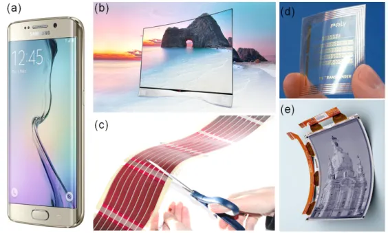
1-1 State-of-of-the-art organic electronic devices, systems, and circuits: a curved OLED display employed in (a) a mobile phone and (b) a television, (c) a flexible and thin OPV module scalable by cut-ting with a pair of scissors, (d) polymer-based RFID tag, and (e) a flexible and lightweight OFET display driving circuit. . . 3 2-1 (a) Hybridised atomic orbitals and chemical bonding in an ethylene
C2H2 molecule. (b) Energy diagram of the carbon-carbon bonding
with the sp2 hybridisation. . . 8
2-2 (a) Hybridised atomic orbitals of benzene (C6H6) molecule. (b)
Chemical structure and energy diagram of benzene. . . 9 2-3 (a) Chemical structure and (b) energy diagram of
poly-para-phenylene-vinylene (PPV). . . 9 2-4 Density of states (DOS) models: square-root, exponential and
Gaus-sian. . . 13 2-5 Categorisation of the density of state and charge transport models
based on the experimental observations on temperature dependent mobility. Correlation between models and organic solid phases is shown. . . 18 2-6 Illustration of the transport mechanisms in solids with applied
elec-tric field. (a) Band-like conduction; electrons are scattered by lattice vibration so that the mobility decreases with increasing temperat-ure. (b) Hopping between localised states; lattice vibration can give electrons chance to overcome the potential barriers (thermally-activated transport . . . 19 2-7 Schematic diagrams for the density-of-states and hole transport
mechanism based on the (a) multiple trapping-and-releasing model and (b) Gaussian disorder model. The symbol Et
bp denotes the
2-8 (a) Energy diagram for an ideal metal/semiconductor junction, where Ebn and Ebp denotes the injection barrier (IB) for electrons and
holes, respectively. (b) The same for a realistic metal/semiconductor junction with the vacuum level mismatch VL and energetic
dis-order. Here, Eo
b is determined in reference to the onsets of the UPS
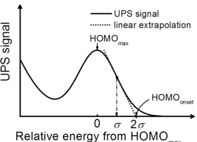
or IPES signals, which are not specific to the density-of-states model. 25 2-9 Schematic diagram of the linear extrapolation method used to
de-termine the onset of the highest-occupied molecular orbitals. The linear extrapolation line is drawn at the inflection point at E = from the HOMOmax. Then, the extrapolation line crosses the base
line exactly at E = 2 from the HOMOmax which is denoted as the
HOMOonset. . . 29
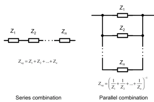
3-1 A graphical representation of the complex impedance plane. . . 31 3-2 Electrical impedance of basic passive circuit elements. . . 32 3-3 Equivalent impedance of a series connection and parallel
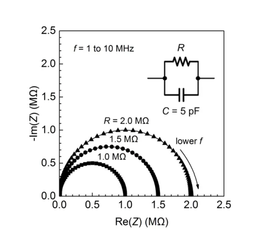
combina-tion of impedance elements. . . 33 3-4 The simulated impedance spectra of RC circuits with a fixed
ca-pacitance and different resistance values plotted on the complex plane. The frequency is from 1 Hz to 10 MHz with the increment of 20 points per decade. . . 34 3-5 The simulated impedance spectra of the inset circuit with a fixed
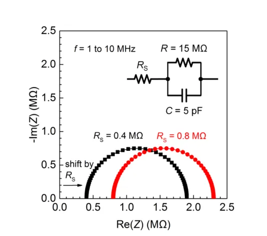
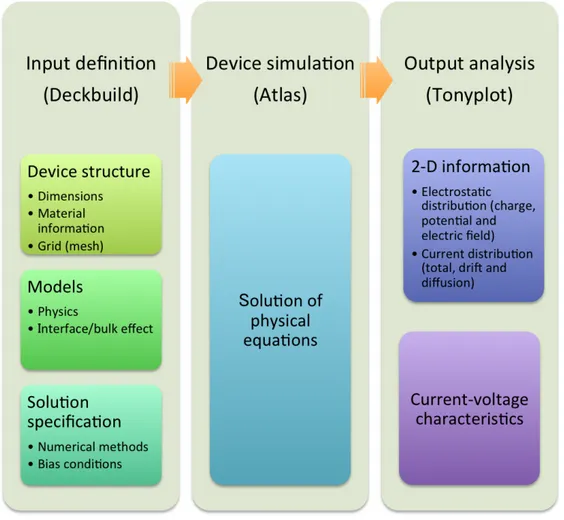
capacitance and parallel resistance with two different resistance val-ues of series resistance plotted on the complex plane. The frequency is from 1 Hz to 10 MHz with the increment of 20 points per decade. 36 3-6 Device simulation process and tasks at each step for 2-D
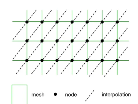
physically-base finite-element simulator. . . 40 3-7 Illustration of the mesh (grid), nodes and interpolation lines in
finite-element method. . . 42 4-1 Schematic diagram of vertical (a) rectifying diode (asymmetrical)
and (b) non-rectifying diode (symmetrical). . . 45 4-2 (a) Energy band diagram of a Schottky junction at thermal
equi-librium: EC conduction band edge, EV valence band edge, and EF
Fermi level. (b) Calculated depletion width as a function of doping concentration at various diffusion potential. . . 48
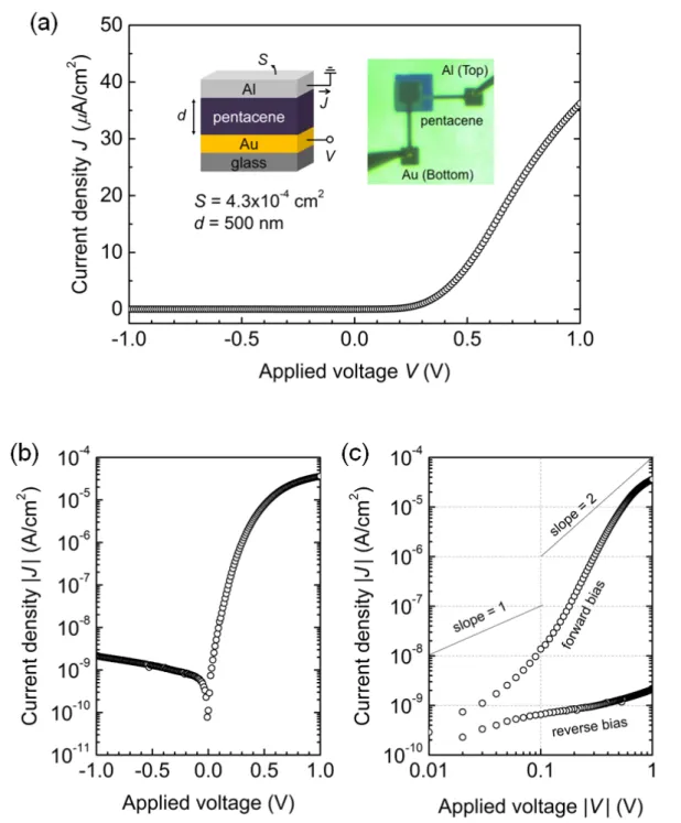
is define as the voltage applied to the Au bottom electrode (anode) in reference to the grounded Al top electrode (cathode). The same results in (b) a semi-logarithmic and (c) double-logarithmic scale. . 49 4-4 Impedance-versus-voltage characteristics of an organic rectifying
di-ode with 500-nm-thick pentacene and Au injecting and Al blocking contacts. . . 50 4-5 Energy diagram of an organic rectifying diode depending on the
strength of injecting contact. The HOMO and LUMO levels are drawn with a solid line for a weaker injecting contact (corresponding to the MIM-model or non-degenerate), and with dotted line for a stronger injecting contact (degenerate). (a) Reverse bias regime, (b) thermal equilibrium, (c) flat-band condition, (d) bulk-limited regime. The lower side arrows indicate the dominant conduction mechanisms under each regime. . . 51 4-6 Device structure and energy diagram of an organic rectifying diode.
Due to the energetic disorder described by the width of the Gaussian DOS ( ), injection barrier Ebpis lowered by 2/2kBT leading to the
effective injection barrier Ee↵
bp. The HOMOedge which is 2/2kBT
above the HOMOmax is analogous to the valence band edge EV for
crystalline semiconductor. The reference points for the position, potential and energy is indicated. . . 54 4-7 Calculated potential profile of a MIM diode with the parameters
listed in Table 4.1 at various applied voltages and for an injection barrier at the anode of (a) 0.46 and (b) 0.26 eV. The applied voltage is varied from 0, 0.3, 0.6 and 1 V. . . 63 4-8 J V curve for a MIM diodes with the parameters in Table 4.1 and
a effective hole injection barrier of 0.46 eV. The solid line correspond to the MIM model, filled circles to the data numerically calculated from the full MIM model, and the dashed lines to the space-charge limited current (SCLC) model (in black) and the linear model J ⇠ V (in red). . . 65
4-9 J V curve for a MIM diodes with the parameters in Table 4.1 and a effective hole injection barrier of 0.26 eV. The solid line correspond to the MIM model, filled circles to the data numerically calculated from the full MIM model, and the dashed line to the space-charge limited current (SCLC) model. . . 65 4-10 Enhancement factors for a Gaussian DOS with dimensionless widths
ˆ = BT = 2, 4, 6, 8 and 10: mobility enhancement by (a) the
charge carrier concentration and (b) by the electric field, and (c) dif-fusion enhancement by the charge carrier concentration. The filled circles in (a) and (c) indicate the concentration where the mobility and diffusion coefficient are enhanced by a factor of 2. The open circles in (c) represents values calculated by a robust semianalytical expression in (4.77)-(4.79). Compared to the direct numerical calcu-lation (solid lines) by (4.75)-(4.76), the calcucalcu-lation error is reduced over a wider range of disorder and charge concentration. . . 68 4-11 Comparison of the current density-voltage characteristics. The
sym-bols represent experimental measurement of the Au/pentacene/Al vertical rectifying diode. The solid line represents the simulation result by the full MIM model with enhanced drift-diffusion. The dashed lines represent the analytical model for reverse bias current with non-degenerate and degenerate approximation and without ap-proximation. . . 73 4-12 Evolution of current density-voltage characteristics upon varying
the width of Gaussian DOS. The same parameters in Table 4.2 are used except the width of the Gaussian DOS varied from 0.16, 0.18, 0.20, 0.22 and 0.26 eV. . . 73 4-13 The hole concentration and potential profile (upper panels) and the
current density and its drift and diffusion components (lower panels) in the device calculated with parameters in 4.2 that gives the best fit to the experimental diode current. Each panel in a row represents different applied voltage: V = -1, 0, 0.3, 0.6 and 1V. . . 75 5-1 Four typical OFET structures characterized by relative positions of
tion. Injected charge carrier must traverse semiconductor layer (ar-rows in violet) to reach channel (arrow in red). (b) Conventional equivalent circuit corresponding to the drain current path. The ac-cess resistance Racc is assumed independent to the gate voltage. (c)
Magnified view of equivalent circuit for current crowding model near source contact. Both the bulk rB and channel resistivity rch have
gate voltage dependence. . . 83 5-3 Simulated (a) hole concentration and (b) potential distribution in
organic semiconductor layer of a staggered OFET under on-state: VGS = -20 V and VDS = -2 V. The channel length is 60 µm, the
semiconductor thickness is 60 nm, and the contact length is 10 µm. Simulated drift-diffusion current (c) across the channel at the source (x =-5 µm) and (d) along the channel (y = 0 nm). The total current (solid line) is the sum of the drift (open circles) and diffusion (filled circles) current. The drift current is dominant along the channel (x = 0 to 60 µm), while both drift-diffusion current have comparable magnitude and opposite sign across the channel. . . 85 5-4 (a) Channel conductivity ch.x and (b) its average on x-axis h ch.xi
(at y = 2 nm), and (c) contact conductivity in the transition zone
c.y and (d) its average on y-axis h c.yi (at x = 5 µm) calculated
at various gate voltage: VGS = 0, 5, 10, 15 and 20 V. Note
the power-law dependence of both channel and contact conductiv-ity with respect to the effective gate voltage. In particular, h c.yi
contains an asymptotic element acc and a power-law dependent
element B. . . 86
5-5 (a) OFET device structure in bottom-gate/top-contact configura-tion. (b) Electronic structures at the contact/organic semiconductor interface. EF denotes the Fermi level, HOMOmax the maximum of
the HOMO, the half-width at half-maximum of Gaussian DOS, and Eb the injection barrier varied as 0.7, 0.8, 0.9 and 1.0 eV. . . . 99
5-6 (a) Simulated transfer characteristics of OFETs. (b) the RonW
-versus-L plot. (c) The ratio ⌘-versus-VGS plot for parameter
extrac-tion (The inset is a close-up view). In the panels (a-c), each symbol represents a different channel length L and each color represents a different injection barrier Eb. (d) The dependence of the extracted
effective threshold voltage Ve↵
T and power-law exponent on Eband
L. Note that Ve↵
T varies significantly with Eb, whereas does not. . 101
5-7 Extracted (a) field-effect mobility µ and (b) contact resistance RCas
a function of effective gate voltage |VGS VTe↵| based on the transfer
length method for several injection barriers. Good fits to power-law mobility and contact resistance models are observed (the solid lines and inset equations). . . 102 5-8 Measured (a) transfer and (b) output electrical characteristics of
a p-type organic field-effect transistor based on pentacene. The solid line represents the parameter extraction by linear extrapola-tion method as well as the ideal drain current model. . . 104 5-9 Ratio ⌘ as a function of VGS calculated for different values of VGS
using (5.39) from the transfer characteristics of a pentacene-based OFET with L = 60 µm (symbols). The solid line is a fit to (5.37) for the extraction of the effective threshold voltage Ve↵
T and power-law
exponent . Dotted lines are a guide to the eye for the asymptotic behaviour calculated by (5.43). . . 104 5-10 RonW-versus-L plot for the TLM. The inset is the equivalent circuit
for the drain current path that consists of the channel and contact resistors (Rch and RC). Both resistors are depicted as a variable
resistor, which emphasizes the modulation of Rch and RC by VGS. . 106
5-11 (a) Mobility and (b) contact resistance as a function of the effect-ive gate voltage |VGS VTe↵| extracted by the TLM. The solid lines
are a fit to the power-law mobility and contact resistance models (inset equations). Thanks to pre-determined parameters by the ra-tio method (Ve↵
T = 12.7 V and = 1.24), all the rest (, A and
R1CW) can be determined by linear extrapolation. Dotted and dash-dot lines correspond to the model of Richards and Meijer, which is a specific case of the proposed model where = 0 or RC = 0. . . 107
fit to the model with power-law RC and µ that leads to the
non-gateable contact resistance R1
C. . . 107
5-13 Comparison between the experimental data with the ideal (I, solid line in black), constant RC and power-law µ (CR, lines red) and
power-law RC and µ (PRM, lines in blue) drain current models in
terms of (a) transfer characteristics and (b) relative difference. . . . 110 5-14 (a) Device structure of a low voltage flexible organic field-effect
tran-sistor and chemical structures of compounds used in the OFET: (b) TIPS-tetracyanotriphenodioxazine as an n-type semiconductor and (c) poly(methyl methacrylate) and (d) 1,6-bis(trichlorosilyl)hexane which form a polymer gate dielectric (e) polysilsesquioxane-PMMA composite. The crosslinking of C6-Si results in polysilsesquioxane
with a three-dimensional structure, which physically confine PMMA reducing the thickness of polymeric gate and increasing the dielec-tric constant, and hence enabling the low-voltage operation. . . 111 5-15 (a) A measured linear-regime transfer characteristics and the
ele-ments of the drain current compact model: above-threshold current Iabove, sub-threshold current Isub and off current Io↵. VT is the
threshold voltage. VB is the voltage at which the difference between
Isub and Iaboveis the minimum. (b) The effect of the transition
para-meter B on the compact model. When VT and VB are a precisely
determined, the model has a large tolerance on B, and it can be defined as B = (VB VT) 1. . . 115
5-16 Final comparison of the compact model with the measured (a) trans-fer characteristics and (b) output characteristics of a flexible low voltage n-type OFET. . . 117
4.1 Parameters used for the calculation of the voltage profile and the current density-voltage characteristics of a MIM diode. ✏0 is the
vacuum permittivity. . . 63 4.2 Parameters used for modelling which gave the best fit to the
exper-imental current density-voltage characteristics. . . 74 5.1 List of Physical Parameters Used for ATLAS Simulation . . . 98 5.2 Comparison of the extracted parameters based on the transmission
length method (TLM) and the single transistor method from penta-cene OFETs. . . 108 5.3 Extracted Parameters from the Modelled TIPS-TPDO-4CN OFETs 118 5.4 Comparison between pentacene versus TIPS-TPDO-4CN
Chapter 1
Introduction
1.1 Organic electronics
Organic electronics, which is also called plastic electronics or polymer electronics, is a branch of electronics making use of electrically conducting and semiconduct-ing polymers and small molecules [1]. The term ‘organic’ is given because the polymers and small molecules mostly consist of carbon atoms with some extent of hydrogen, oxygen, nitrogen, sulfur, phosphor or heavy metal atoms incorporated to endow functionalised characteristics to polymers and molecules. This is the most significant difference compare to conventional electronics, in which inorganic semiconductors, such as silicon (Si), gallium arsenide (GaAs), etc. are used. In 1862, H. Letheby obtained a weakly conducting polymer though anodic oxidation of aniline in sulfuric acid, which was thought to be polyaniline [2]. After the report in 1977 [3], which stated that polyacetylene can be oxidized with halogens to pro-duce materials with a wide range of conductivity from an insulator to a conductor, research on conducting polymers gained much more attention. On the other hand, researchers discovered conducting organic molecules in the 1950s. For example, a semiconducting charge-transfer complex, perylene-iodine which is a kind of salts consists of polycyclic aromatic molecules and halogens, with high conductivity of 0.12 S/cm was reported in 1954 [4]. These demonstrate that electrical current can pass through organic polymers and molecules.
Since the discovery of conducting and semiconducting properties, organic semi-conductors have been used actively in various electronic and optoelectronic devices. First, organic polymers and molecules were adopted in solar cells, and the earlier and recent progress in organic solar cells (OSCs) are well summarized in the art-icles [5–7], which have been made since the first observation of photoconductivity in organic semiconductors reported in 1950s [8,9]. Second, there have been a large
number of reports demonstrating the use of organic materials for organic light-emitting diodes (OLEDs) since the pioneering work by C. W. Tang [7]. Third, polythiophene which is a class of organic conjugated polymers discovered in the late 1970s was successfully introduced in organic field-effect transistors (OFETs) by Koezuka and coworkers in 1986 [10, 11].
One of the most distinctive features of organic materials is given by their mo-lecular nature. In contrast to inorganic crystals that consist of atoms held in place by covalent bonds, organic solids are formed by molecules or polymers bound by van der Waals force. Thanks to this weak van der Waals force [1], organic solids possess mechanical flexibility (Young’s modulus lower than a few tens of GPa) and solids can be assembled more easily. The latter means that organic layer can be formed from solution containing an organic semiconductor and proper solvent (called organic ink) or evaporated at a moderate temperature (below a few hun-dreds of C). In particular, printed organic electronics, which combines organic ink and conventional ink jet printing technique, holds a clear advantage of being able to control the deposition of functional layers only at desired points on the sub-strate and to reduce of material waste and process time compared to conventional shadow masking and lithographic patterning techniques [12,13]. On this account, the subsequent progress has been made towards realization of ‘large-area’, ‘flexible’ and ‘low-cost’ electronic systems.
We have seen impressive progress in organic electronics over recent years. Amongst them, OLEDs are remarkable for diverse products already available or in the prototype phase. OLED’s display application showed particularly significant success. Owing to their inherently wider color gamut, moving-picture response, and low power-consumption, OLEDs are replacing conventional liquid-crystal dis-plays (LCDs) not only in mobile devices but also in consumer electronic devices. Figure 1-1(a)-(b) shows a curved OLED display mounted on a commercial mobile phone produced by Samsung Electronics (2015) [14] and a television produced by LG electronics (2016) [15]. Another key application of OLEDs in the future might be solid-state lighting by white (or coloured) OLEDs with a particular articulation on the uniform light emission from a large surface area [16–18]. OPVs for generat-ing electrical power from sunlight are a particularly important application due to increasing demand for environmentally benign energy production. Infinitypv [19] has demonstrated various types of printed OPV modules with excellent flexibility, scalability (1 ⇠ 4 W/m) and light weight (220 ⇠ 450 g/m2) Figure 1-1(c).
Or-ganic diodes and OFETs can be used for various circuit applications. PolyIC [20] demonstrated a polymer based RFID tag Figure 1-1(d). OFETs are adopted in
1.1. ORGANIC ELECTRONICS
Figure 1-1: State-of-of-the-art organic electronic devices, systems, and circuits: a curved OLED display employed in (a) a mobile phone and (b) a television, (c) a flexible and thin OPV module scalable by cutting with a pair of scissors, (d) polymer-based RFID tag, and (e) a flexible and lightweight OFET display driving circuit.
active-matrix pixel drivers in LCDs or OLEDs, and OFET-based display back-planes are under consistent development [21, 22]. Plastic Logic’s ultra-flexible paper-like display in Figure 1-1(e) has developed a backplane circuitry composed of OFET arrays [23]. OFET-based large-area sensors for optical and mechanical read-out are also significant for advanced applications such as conformable image scanners, electronic skins [24–27].
Today, organic electronics is still actively evolving. Researchers have overcome many critical challenges encountered at its infancy, such as performance and sta-bility issues. However, the industrial acceptance seems not prompt probably due to pre-existing or other emerging technologies, especially where the unique advant-ages of organic semiconductors are diluted (i.e. market takeover). More recently, the concepts of creating new-market or targeting niche-market are also emphas-ized, and novel applications are continuously being envisaged. Encouraged by multidisciplinary character of organic electronics, physicists, chemists and engin-eers are exploring a wide range of new materials and device functionalities, which led to the conceptualisation of various new of organic devices. Amongst them, biomedical application is regarded as one of the most attractive orientations that organic electronics community can proceed toward [28, 29]. A variety of initiative works on chemical and biological sensors are being reported [30]. We anticipate a
further advancement that will promote organic electronics to a more competitive position, where attractive features of organic semiconducting materials will be in full bloom.
1.2 Motivation
The foremost motivation of this thesis is the lack of mature theoretical under-standing on organic semiconductors and devices. Because it provides a reliable, comprehensive, and well-documented knowledge base, conventional microelectron-ics still represents the main source for modelling, interpreting, and conceiving organic electronic devices. However, a considerable amount of theoretical and ex-perimental effort has been carried out during the recent decades to develop more adequate models to account for the specificities of organic semiconductors. In pursuit of physical modelling, the material aspect has been the principal concern, such as the effect of aforementioned molecular nature of organic solids on the elec-tronic structure, and concomitant charge carrier transport and injection processes. Unique features of these processes in organic disordered semiconductors (ODSs) are being continuously discovered by physical modelling (such as ab-initio approach based on Monte-Carlo simulation method or a direct numerical solution of physical equations) of a simple organic semiconductor medium and/or metal/organic semi-conductor junction. For example, the concept of describing the density-of-states as a random distribution of localised states was introduced [31]. In addition, the dependence of mobility, a transport parameter, on surrounding conditions such as lattice temperature, charge carrier concentration and electric field has been high-lighted [32, 33]. Nonetheless, these recent findings have not been fully addressed to the device-level physical modelling mainly due to its mathematical complex-ity and two- or three-dimensional structures of actual devices. As a consequence, correlation between the result of physical device modelling and the experimental data is still lacking. The former is indeed highly recommended in that it enables validation or refinement (that may need) of the model, facilitates interpretation or even predictions of experimental results, and provides feedback for an improved device design and fabrication process control.
The second motivation is to develop a physically-based compact model that is sufficiently simple for it to be adopted in circuit simulators and sufficiently accurate for the result of modelling to be useful for circuit designers [34]. During past decades, there has been a growing interests in integrating organic electronic devices (i.e. single diodes or transistors) into a circuit or system (single diodes or
1.3. THESIS OVERVIEW transistors. display driving circuit, PV modules, RFID system and matrix-based sensors). In this context, the necessity of a physically-based compact model is getting more recognised. In circuit simulators such as SPICE (Simulation Program with Integrated Circuit Emphasis) [35], device characteristics are represented by an equation (or a set of equations). In this case, directly adopting the genuine physical modelling that often requires iterative numerical calculation might not be a suitable choice. Therefore,it is necessary to examine and employ an analytical or empirical approach, such as through physical approximations or parametrisations, in order to achieve the required level of simplicity of the compact model for a device. A related work for optimising the trade-off between the simplicity and physical rigorousness is also required. In summary, a reliable compact model will serve as an intermediary between the device-level and the circuit level modelling practices.
1.3 Thesis overview
This thesis is titled ‘physically-based compact modelling of organic electronics devices’. Mathematical device modelling is developing a numerical or analytical model that describes the behaviour of the electrical devices. As the title implies, our principal goal is to develop specific models for organic devices that possess both physical basis and practical applicability. These two aspects are in line with the two major motivations described above. In this context, we paid a balanced effort in reviewing a wide range of charge carrier transport and injection physics as well as theoretical and experimental methods (Chapter 2 and 3), and adopting them into the compact models of typical devices (Chapter 4 and 5). Here, a short description of each chapter is given for overview.
Chapter 1 Introduction outlines a field of organic electronics, explains the motivations for the thesis and related aim and scope of the thesis.
Chapter 2 Fundamentalsprovides short summaries on the most basic phys-ical backgrounds required for understanding organic semiconductors and electronic devices. The origin of the semiconducting properties in organic materials is ex-plained briefly. Square-root, exponential and Gaussian DOS models are presented for describing how energy states are distributed in organic solids with different degrees of crystallinity. Related charge carrier transport physics are delineated, defining a clear boundary of its pertinence. The effect of disorder on charge carrier injection at metal/organic semiconductor interface is demonstrated.
meth-ods used for the analysing and modelling organic electronics devices. A basic in-formation on impedance spectroscopy, analytical modelling, numerical modelling, and experimental validation is given, focusing on the complementary functions between each methods. Special considerations for practice are presented which has been key factors for obtaining a reliable result.
Chapter 4 Organic diodes is the first chapter devoted to the scientific res-ults. Organic rectifying diodes are studied by means of theoretical and experi-mental techniques. The concept of full-depletion in unintentionally-doped organic semiconductors is presented, and its limit in relation to the charge injection is de-scribed. The theoretical development for the electrostatic distribution and current-voltage characteristics are elaborated in the weak and strong injection conditions. Chapter 5 Organic field-effect transistors (OFET)is the second chapter devoted to the scientific results. OFETs having staggered geometry are invest-igated. Numerical modelling results are presented for understanding the current path in the transistor, identifying the origin of the contact voltage drop and power-law gate voltage dependence of contact resistivity. A modified equivalent circuit based on current crowding model is presented that leads to power-law mobiltiy. Theoretical and experimental evidences are provided to support the existent of power-law dependent mobility and contact resistance in the OFETs with Gaus-sian DOS and hopping transport. Such phenomena is newly introduced into the drain current model and related parameter extraction method, maintaining the physically-based compact modelling philosophy.
Chapter 6 Conclusion and perspectives summarise major results found and analysed in the thesis with concluding remarks. Limitations of the presented work and suggestions for the further investigation is also specified.
Chapter 2
Fundamentals
In this chapter, fundamental physics of organic semiconductors and charge trans-port and injection processes is summarized. We focused on emphasizing distinct features of organic materials and devices, providing concise comparison with the inorganic counterparts. For basic knowledge on solid-state physics and semicon-ductor device physics, we recommend referring to typical textbooks [36–38]. First, we discuss the semiconducting property and electronic structure of organic ma-terials. Then, the charge carrier transport is elaborated illuminating how dif-ferent density of states (DOS) models and/or transport mechanisms of organic materials could explain experimentally observed mobility behaviours. Finally, en-ergetic alignment and formation of the carrier injection barrier upon forming a metal/organic semiconductor junction is described.
2.1 Organic semiconductor
2.1.1 ⇡-conjugated molecules and polymers
Organic semiconductors are a class of organic compounds that possesses a semi-conducting property, i.e. organic small molecules or polymers, made up by carbon and hydrogen atoms and at times heteroatoms such nitrogen, sulfur and oxygen.
Carbon is a group four element in the periodic table with four valence elec-trons accommodated individually in 2s, 2px, 2py and 2pzatomic orbitals. A special
property of carbon is the ability to hybridise its atomic orbitals upon bonding with other atoms. Three different ways are possible according to the number of direc-tional p atomic orbitals engaged in the hybridisations: sp1, sp2 and sp3, which leads
to a wide variety of bonding configurations [1]. In particular, sp2-hybridisations
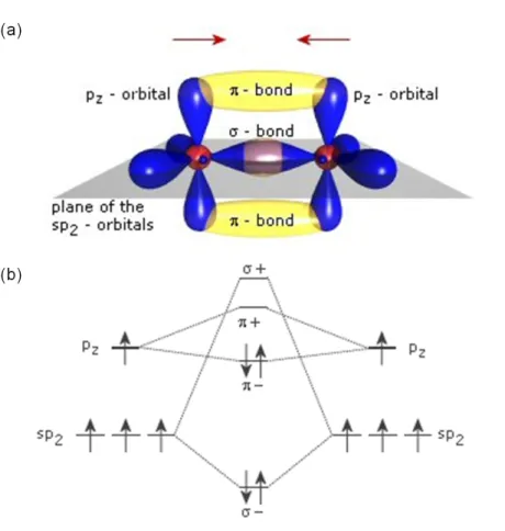
-Figure 2-1: (a) Hybridised atomic orbitals and chemical bonding in an ethylene C2H2 molecule. (b) Energy diagram of the carbon-carbon bonding with the sp2
hybridisation.
orbitals are in the plane perpendicular to it. The simplest example of this kind is ethylene C2H2 Figure 2-1(a). When two carbon atoms with sp2-hybridisations
approach, a large orbital overlap of two sp2-orbitals forms a strong -bond. The
energy difference between the occupied binding orbitals ( +) and the unoccupied anti-binding orbitals ( -) is quite large and well beyond the visible spectral range. Correspondingly, longer chains of bound carbon atoms would have a large gap between the highest occupied molecular orbital (HOMO) and the lowest unoc-cupied molecular orbital (LUMO), leading to insulating properties Figure 2-1(b). On the other hand, in the sp2-hybridisations, two pz-orbitals form additionally
⇡-bonds. These bonds have much smaller energetic difference between the HOMO and LUMO, leading to strong absorption in or near the visible spectral range and to semiconducting properties. Therefore, in principal, organic compounds that have frontier orbitals (HOMO and LUMO) formed by ⇡-bonded electrons are con-sidered as semiconductors.
2.1. ORGANIC SEMICONDUCTOR
Figure 2-2: (a) Hybridised atomic orbitals of benzene (C6H6) molecule. (b)
Chem-ical structure and energy diagram of benzene.
Figure 2-3: (a) Chemical structure and (b) energy diagram of poly-para-phenylene-vinylene (PPV).
picture of benzene (C6H6). Because there exist 3 pairs of pz-orbitals to form
⇡-bonds compared to 6 pairs of sp2-orbitals in the ring, it was represented by an
alternating single and double bonds in the conventional chemical structure. How-ever, all the six electrons coming from the six carbon pz orbitals are so weakly
bound to the neighbouring atoms that they are in effect delocalised through the whole cyclic chain of the molecule, giving rise to geometrical symmetry. An-other important aspect demonstrated by the benzene molecule is the split of the binding and anti-binding orbitals into close but different energy levels shown in Figure 2-1(b). This is analogous to the formation of energy bands of inorganic semiconductors when the number of atoms increases to make a crystal network. Thus, it can be said that the HOMO and LUMO ‘levels’ widen into the HOMO and LUMO ‘bands’, which are often interchangeably used with the valence band and the conduction band, respectively. The gap between occupied and empty states in these ⇡-systems becomes smaller with increasing delocalisation, leading to absorption and fluorescence in the visible. Also, thanks to higher molar mass, these substances can be prepared as solid.
If a long chain of carbon atoms is formed, the ⇡-bonds become delocalised along the chain and form a one-dimensional electronic system. This type of chemical system where the ⇡-electrons are delocalised through alternating single and double bonds is often called a ⇡-conjugated system. Figure 2.3 shows an example of the ⇡-conjugated polymer, poly-para-phenylene-vinylene (PPV). In general, as the conjugation length increases, the bandwidth increases and the band-gap decreases as a result of the splitting of the frontier molecular orbitals. Polymer organic semiconductors are usually deposited in wet processes, like spin-coating or printing.
2.1.2 Material classification
Organic semiconductors are most frequently categorized as small molecules or poly-mers based on the size and molecular weight. In contrast to a defined chemical structure of an organic small molecule an organic polymer has dispersion in size and molecular weights according to the number of repeating units. Despite the differences in the size-originating properties, they share a common feature of al-ternating single and double bond, ⇡-conjugations, for a semiconducting property. The second criteria for classifying organic semiconductor is solubility which determines the type or easiness of deposition process. Although polymers has been regarded as a soluble material and preferably used for solution process [39,40], the solubility of small molecules has been improved by strategic synthesis including the attachment of substitution groups that enhance solubility [41, 42]. Now, selective
2.1. ORGANIC SEMICONDUCTOR solubility to a specific solvent, namely orthogonality, is regarded as a key factor for achieving successive deposition of organic layer on top of pre-existing organic layers without damaging the latter [43, 44].
The third criteria is the conduction type of the organic semiconductor either p-type (hole-transporting) or n-type (electron-transporting). This should not be confused with the same denomination used for inorganic semiconductors. Since inorganic semiconductors are generally used in a doped form, the appellation of p-or n-type is based on the type of doping impurities: p-type inp-organic semiconduct-ors are doped by acceptor impurities, and n-type by donsemiconduct-ors. In contrast, organic semiconductors are used mostly without intentional doping. In effect, it is not the type of dopant but the type of ‘injected’ charge that determines the type of conduction in organic semiconductor. This was evidenced in OFETs by the min-imum difference between the electron affinity of organic semiconductor and work function of source and drain contact metal to achieve n-type conduction [45].
Since the first discovery of p-type organic semiconductor, the vast majority of demonstration have been concerned with is p-type organic semiconductor and devices. The n-type OFETs are especially useful for organic complementary cir-cuits (OCCs). Indeed, compared to the unipolar circir-cuits based only on p-type OFETs, the use of both n- and p-type OFETs enables larger noise margin and lower power consumption [46, 47]. At its infancy, n-type organic semiconduct-ors, such as lutetium diphthalocyanine [48], C60 [49, 50] or those bearing electron
withdrawing groups such as cyanide [51] or imide [52, 53], suffered from highly sensitive to ambient air, humidity and light. Over the past two decades, develop-ing a n-type organic semiconductor with good stability and electron-transportdevelop-ing behaviour has been one of the first priorities for the improvement of the material property [54–59]. Among them, the perylene and naphthalene carboxydiimide de-rivatives are two famous families of n-type organic semiconductors [60–64]. Also, electron-transporting triphenodioxazine (TPDO) derivatives, which can be pro-duced at the industrial scale, have gain significant attention [65, 66].
2.1.3 Organic solids
At variance with inorganic semiconductors, where covalent bonds between atoms are the only contribution to the formation of macroscopic crystal of solid, organic molecules are bounded by weak van der Waals force [1], which means that semicon-ducting properties at the macroscopic level is possible only if the inter-molecular interaction is significant for the ⇡-conjugated electrons can be delocalised and moved from one molecule to another. This brings both unique opportunities and
ultimate limitations to device applications.
The process temperature of an electronic device can be significantly lowered through simple evaporation or printing techniques. Even, deposition of functional organic materials on a plastic or rubber-like substrate for flexible and even stretch-able electronics [67–70]. On the other hand, due to the weak electronic coupling between molecules, there is a significant limitation to the charge-carrier transport, as discussed in more detail in Section 2.3.
For illustrative purposes, organic semiconductors exist in form of molecu-lar crystals, polycrystals or amorphous thin films with different long-range of disorder. Organic single crystals can be obtained either from small-molecules through physical vapour transport method under controlled pressure and tem-perature gradient [71–73] or through solution growth [74] as a free-standing single crystal piece or as a thin-film deposited and fixed on a substrate. Organic poly-crystals and amorphous can be obtained vacuum evaporation or solution-based techniques mostly as a thin-film [75]. This implies that inter-molecular interaction of organic solid and concomitant physical processes varies significantly according to the macroscopic morphology of the solid.
Considering that a majority of organic electronic devices is composed of or-ganic solids, despite existence of a single molecule or polymer-based electronic devices [76–78], understanding the effect of macroscopic morphology on various semiconductor properties (structure-property relationship) constitutes the core of organic semiconductor material and device physics.
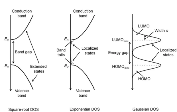
2.2 Density-of-states models
In order to understand charge carrier transport and injection in organic solids, we need to elaborate on the electronic structure of organic solids. The density-of-states (DOS) model describes the shape and characteristics of the electronic structure. We will present representative DOS models for different degree of solid phases: square-root extended band with and without localised exponential trap-states (namely, square-root and exponential DOS models) and Gaussian DOS model, respectively for crystalline, polycrystalline and amorphous phases (Fig-ure 2-4). We note that the first two models were conceived from inorganic crystals and polycrystals and have been frequently adopted for organic semiconductors, which would be legitimate for highly crystalline organic solids. At present, there is increasing consensus on Gaussian DOS as a more pertinent description for energy structure of organic disordered semiconductors (ODS). This section is dedicated
2.2. DENSITY-OF-STATES MODELS
Figure 2-4: Density of states (DOS) models: square-root, exponential and Gaus-sian.
to illustrate the fundamental differences between each model and underlying as-sumptions of each model, reserving a more conclusive remark for Section 2.3.
2.2.1 Square-root density-of-states
A complete description on energy bands in solids is found in several text books [36, 37]. Here, we will limit our scope to the energy band of the representative inorganic semiconductor, single crystal silicon (c-Si).
Free-electrons in a Fermi gas of 3-D system results in density of states following parabolic shape. For electrons and holes
DC(E)/ p E EC, (2.1) DV(E)/ p EV E, (2.2)
where EC and EV are the conduction band and valence band edges, respectively.
The ‘sharp edge’ signifies that the DOS does strictly fall to zero at E = EC and
E = EV and takes zero value in the energy gap (EV < E < EC).
Then, the charge carrier concentration is determined by integrating the product of the DOS function and the Fermi-Dirac distribution function for electrons fF D(E,
EF) = 1/[1 + exp((E EF)/kT )]or for holes [1 fF D(E, EF)]:
n = Z 1
1
D(E)fF D(E, EF)dE, (2.3)
p = Z 1
1
D(E) [1 fF D(E, EF)] dE, (2.4)
where EF is the Fermi energy, k Boltzmann constant and T the temperature.
Al-though the integration does not lead to an analytical result in the general case, the following very simple approximate solution emerges at low charge carrier density, when the Fermi level is sufficiently far from the band edges:
n = NCexp ✓ EC EF kT ◆ , (2.5) p = NVexp ✓ EF EV kT ◆ , (2.6)
where NC and NV are the effective density of states at conduction and valence
band edge, respectively. For silicon at room temperature, NC = 2.9⇥ 1019cm 3
and NV = 1.04⇥ 1019cm 3. Under such circumstances, the semiconductor is said
to be in the non-degenerate regime.
Ultraviolet photo-emission spectroscopy (UPS) and inverse photo-emission spec-troscopy (IPES) are the methods of choice to determine the energy structure of semiconductors. Inspired by the first work on the external photoelectric effect of metals by Einstein [79] and the same of semiconductors by Condon et al. [80], Apker et al. not only determined the position of the valence band edge but also demonstrated that the density-of-states in the valence band can be experimentally deduced from the energy of photoelectrons [81]. These initial works on photo-electrons support the band theory for crystalline semiconductors providing a link between the existence of the band edge with the sharp cut-off of stopping potential from photo-emission measurement.
2.2.2 Exponential density-of-states
Disorder in amorphous silicon gives rise to the localisation of the states. Anderson described in [82] that when disorder is introduced in a regular crystal structure extended states gradually change to localised states. The lack of long-range order results in the loss of sharp band edges so that the density of states shows a tail of localised states extending into the energy gap [83, 84]. The degree of localisation can be quantified by comparing the amount of disorder to the width of the energy
2.2. DENSITY-OF-STATES MODELS band.
In silicon, the conduction and valence bands have a width around 5 eV, so the degree of disorder in amorphous silicon is weak [85]. As a consequence, there still exist extended states; as shown in Figure 2-4, localised states appear as band tails inside the energy gap. These tails are usually described as an exponential density of states referring to the energy of photoelectrons from amorphous silicon proposed by Peterson et al. [86]. It is experimentally determined from the onset of the UPS or IPES signals and considered to indicate the same position as the band edge of the same semiconductor in its crystalline phase [87, 88]. Mathematically, thus, the total DOS is represented as the sum of band and exponential tail DOSs, D(E) = DC(E) + DTC(E) + DV(E) + DTV(E), with
DTC(E) = NTC kTCC exp ✓ E EC kTCC ◆ E < EC, (2.7) DTV(E) = NTV kTCV exp ✓ EV E kTCV ◆ EV < E, (2.8)
where TCC and TCV are characteristic decay temperature describing the
distribu-tion of trap states, NTC and NTV are conduction and valence band edge intercept
densities.
2.2.3 Gaussian density-of-states
The foremost difference between typical inorganic and organic semiconductors is the binding energy between the elemental constituent of the solid: weak van der Waals interaction in organic solids versus strong covalent binding in silicon. As a direct consequence, the width of the valence (HOMO) and conduction (LUMO) bands is two orders of magnitude lower in organic semiconductors typically of order 0.1 eV [89]. This is about one order of magnitude larger than the corresponding transfer integrals [89], meaning that all the states are now localised with the local-ization centres being molecules or molecular subunits, called herein sites [89–92].
Because the site energies, which are to a great extent determined by electronic polarization, are mainly controlled by disorder, the density of states in organic disordered semiconductors (ODS) (i.e. non-crystalline that is most of them to the exception of single crystals) can now be safely approximated to a Gaussian distribution function. For simplicity, we will develop equations only for holes in
the HOMO. The Gaussian DOS of the HOMO is written as g(E) = pN0 2⇡ exp ( (E HOMOmax)2 2 2 ) , (2.9)
where is the width of the distribution, N0 is the total density-of-states per unit
volume and HOMOmax is the energy level in the HOMO at which the DOS is the
greatest. In general, we take the density of molecule for N0 [93].
The hole concentration is estimated in a similar manner to (2.4): p =
Z 1 1
g(E)fF D(E, EF)dE. (2.10)
Under Boltzmann’s approximation, the hole concentration has analytical form: pndeg = N0exp 1 kBT ⇢ EF ✓ HOMOmax+ 2 2kBT ◆ . (2.11) At this point, it is worth pointing out a specificity of the Gaussian DOS, first analysed in details by Tessler and Roichman [94]. A remarkable outcome of this investigation was that the Gaussian DOS only leads to the simple non-degenerate equations (2.11) at very low charge carrier density, when the Fermi level is far from the maximum of the DOS. For higher concentrations, as those seen in the accumulation layer of field-effect transistors or in doped organic semiconductors, the dependence of p with EF is no longer analytical; this is more pronounced
as the width of the Gaussian distribution is large. Nonetheless, approximation of the Fermi-Dirac distribution function to a Heaviside step function, for holes fH(E, EF) = 1for E < EFand 0 for EF < E, we have a semi-analytical expression:
pdeg = N0 2 erfc EF HOMOmax p 2 , (2.12)
where erfc(x) is the complementary error function.
Recently, Paasch [95] established semi-analytical approximations for the charge carrier concentration dependent to the Fermi level by merging (2.11) and (2.12) with transition functions H(ˆ) and K(ˆ) given by
H(ˆ) = p 2 ˆ efrc 1 exp ✓ ˆ2 2 ◆ , (2.13) K(ˆ) = 2 ( 1 H(ˆ) ˆ r 2 ⇡exp 1 2ˆ(1 H(ˆ) 2) ) , (2.14)
2.3. CHARGE CARRIER TRANSPORT where erfc 1(x)is an inverse complementary function and ˆ = /kT is the reduced
dimensionless width of Gaussian DOS. We have, for holes,
pPaasch = 8 > > > > > > > > > > > < > > > > > > > > > > > : N0exp ✓ EF r ˆ2 2 ◆ 1 + exp [ K(ˆ)(EF r ˆ2)] EF r> ˆ2 (2.15) N0 2 exp ✓ ˆ2 2 ◆ EF r= ˆ2 (2.16) N0 2 erfc EF r p 2ˆH(ˆ) EF r< ˆ 2 (2.17)
where EF r is the reduced dimensionless Fermi level and width of Gaussian DOS
defined by EF r= (EF HOMOmax)/kT.
2.3 Charge carrier transport
Charge carrier transport is a movement of charge carrier in space with electric potential gradient. Distinctive characteristics of charge carrier transport in or-ganic solids are closely related with their electronic structure. Thus, it requires a unique model that could take into account the molecular nature of organic solids. Moreover, a real challenge exists in understanding and developing charge carrier transport models covering a large number of material classes that have differ-ent energetic configurations related to the molecular structure itself and also the process-dependent film microstructure.
The temperature dependence of mobility has been regarded as indicative for the DOS model as well as the transport model. Figure 2-5 shows a simplified categorization of the observed temperature dependence of mobility according to the density of state and charge transport model as well as organic solid phase. A detailed description will be given in the following.
2.3.1 Band transport model
The band conduction of delocalised electrons is described by Drude’s free electron model [36,96]. The model describes the drift of charge carriers placed in an applied electric field as a repeated process of acceleration and collision with the lattice through which they lose completely their energy. This process results in an average drift velocity proportional to the electric field strength, from which the constant
Figure 2-5: Categorisation of the density of state and charge transport models based on the experimental observations on temperature dependent mobility. Cor-relation between models and organic solid phases is shown.
of proportionality is defined as mobility µ by µ = F vth = q⌧ m = q m mvth (2.18)
Here, q is the elementary charge, m is the effective mass, ⌧ is the mean time between lattice collisions, m the mean free path, and vth the thermal velocity.
As illustrated in Figure 2-6(a), band transport is not thermally activated because increasing temperature reduces m and µ. This behaviour is usually modelled by
µ/ T n with n > 0 [36], where T is the absolute temperature.
2.3. CHARGE CARRIER TRANSPORT
Figure 2-6: Illustration of the transport mechanisms in solids with applied electric field. (a) Band-like conduction; electrons are scattered by lattice vibration so that the mobility decreases with increasing temperature. (b) Hopping between localised states; lattice vibration can give electrons chance to overcome the potential barriers (thermally-activated transport
general parameters put into 2.18 give µ of the order 100 cm2V 1s 1 or higher [36].
In other words, the primary assumption of Drude’s model fails for organics because µ < 1 cm2V 1s 1 corresponds to a value
m smaller than the lattice spacing
(in-termolecular distance). Therefore, we consider that genuine band transport is not relevant to organic semiconductors, and it might be restricted to highly-pure and defect-free single crystals at extremely low-temperature [73, 97, 98]. As temperat-ure increases, intra- and intermolecular vibrations destroy the coherence between adjacent sites, which makes a charge carrier scattered with a mean free path that approaches the distance between adjacent sites. As a result, band transport is no longer possible and a charge moves through a different transport mechanism, i.e. thermally assisted hopping to be discussed.
It is for this reason that occasional experimental observation of a negative temperature coefficient (dµ/dT < 0) in low-mobility organic crystals is generally described by the band-‘like’ transport. The exact origin of this mechanism has not been fully understood yet [99–102].
2.3.2 Polaronic transport model
When the charge localization effect is pronounced, the transport is described by the hopping between localised states. In this case, because the lattice vibration helps localised charges to escape the potential well, transport is assisted by thermal energy (dµ/dT > 0) as shown in Figure 2-6. In general, two origins of localisation are considered; polarization and disorder.
Electronic polarization indicates local deformation of the charge density due to the additional charge staying at this location [75]. This leads to an immediate relaxation of that particular state by the induced potential. As a consequence, the further motion of the staying charge is hindered, thus called the self-trapping effect. Once this charge moves to another molecule (or a segment of molecule), this effect takes place again. Therefore, this type of charge transport is visualised by a collective movement of a charge and its accompanying polarization (of the opposite sign) which are called a ‘polaron’.
Polaronic transport is a distinctive feature of all organic semiconductors. Be-cause of small transport bandwidth, residence time becomes longer than polar-ization time. Also, because of small dielectric constant of organic materials, the localizing potential gets intensified.
2.3.3 Multiple-trapping and release (MTR) model
The second mechanism of localisation is induced by energetic and geometrical dis-order. We will first discuss the case when the degree of disorder is not significant (compared to the transport bandwidth), namely ‘weak localisation’. In this case, the energy structure is best represented by the DOS model of the extended band with localised exponential trap states (2.8). This picture is widely-used in conven-tional model for amorphous silicon (a-Si) [103, 104]. For organic semiconductors, organic solids with poly-crystalline phase can be generally well described by this model. They can form relatively well-ordered small domains with different ori-entation between domains. The main origin of localised tail states in a-Si are dangling bonds, and that in polycrystalline organic semiconductors can generally be attributed to the grain boundaries [105].
In this energetic situation, the charge-transport is based on the multiple trap-ping and release (MTR) process illustrated in Figure 2-7. In this model, it is assumed that most of the charge carriers are trapped in localized states, and the charge carrier transport is manifested only by the temporarily released charge car-riers to an extended-state transport level (above the valence band edge for classical
2.3. CHARGE CARRIER TRANSPORT p-type semiconductors, i.e. mobility edge), the amount of which depends on the electronic structure of the localized states, temperature and injection. Therefore, the MTR model adopts the DOS model of the extended band with localised ex-ponential trap states in (2.8).
A detailed analytical formulation for obtaining trapped and free charge carrier density will be given in [105]. Here, for discussion purpose, we simply present the expression of the effective mobility µMTR determined by the trapped-to-total
carrier density, µMTR = µ0 pf pf + pt ' µ 0 NC NT exp ✓ EF EV kT ◆ (2.19) where µ0 is the band mobility, pf the free hole density, pt the trapped electron
density, NC the effective DOS at the conduction band edge, EF the Fermi level,
and k the Boltzmann constant. We assume EC kT and pt pf for (2.19). The
key feature of (2.19) is Arrhenius temperature dependence for thermally activated charge transport:
µ(T )' µ0exp
kT , (2.20)
2.3.4 Variable-range hopping model
Now, we will discuss the case when the degree of disorder is significant. The basic ideas of variable-range hopping can be briefly formulated as follows: charge trans-port in organic disordered semiconductors is manifested by incoherent hopping of charge carriers in randomly distributed localised states i.e. the Gaussian DOS.
The hopping rate (or the jump rate) is a key element of this model. It considers the high localization of charge carriers in disordered organic materials (sites) and its effect on charge transport. The jump rate of a carrier between two localised sites i and j is assumed to be of the Miller-Abraham type [31,89], [90–92,106,107], i.e., it is the product of a prefactor ⌫0, a carrier wave-function overlap factor, and
a Boltzmann factor for jumps upward in energy. ⌫ij = 8 < : ⌫0exp ✓ 2↵rij Ej Ei kT ◆ Ej > Ei, (2.21) ⌫0exp ( 2↵rij) Ej Ei, (2.22)
Here ⌫ij is the rate for the hop between an occupied site, i, and an empty site, j,
separated by distance rij; ↵ is the inverse decay length of the carrier wave function
Figure 2-7: Schematic diagrams for the density-of-states and hole transport mech-anism based on the (a) multiple trapping-and-releasing model and (b) Gaussian disorder model. The symbol Et
bp denotes the transport based definition of the IB.
hopping rate); k is the Boltzmann constant.
In essence, describing the distributions of sites in space ri and energy Ei is a
central quest for the description of charge transport under the hopping model. If spatial positions and energies of localised states can be considered independent from each other, this model is traditionally called the Gaussian Disorder Model (GDM) [31]. Until recently, the effect of the distribution of sites in energy has been actively investigated, upon assuming the uniform distribution of sites in space, rij ⇡ r. In particular, the structure of the DOS in ODSs is probably the most
controversial issue in research on these materials. The discussion is mostly focused on whether the DOS is Gaussian as described by 2.8or exponential in the form given by 2.9 [33]. In order to evaluate the pertinence of each DOS model, the mobility (an observable parameter) is determined from the hopping rate, and its dependence on environmental factors, such as the temperature T , charge carrier concentration p and electric field F , are compared to the experimental observations.
The first merit of adopting the Gaussian DOS delineated in previous reviews [31, 33] is based on the temperature dependence of the carrier zero-field mobility µ(T ), measured in time-of-flight experiments at low carrier concentrations.
Experi-2.3. CHARGE CARRIER TRANSPORT mental data for carrier mobility in ODSs at low carrier concentrations demonstrate a strong temperature dependence in the form [33, 92, 108–110]
µ(T )' µ0exp " ✓ T0 T ◆2# , (2.23)
with properly adjusted parameters T0 and µ0. At high carrier concentrations,
particularly in OFETs, the dependence µT often has the Arrhenius form with a
weaker temperature dependence [111] well known also for inorganic disordered semiconductors, such as chalcogenide glasses and amorphous silicon. While the hopping transport in a Gaussian DOS exhibits both non-Arrhenius and Arrhenius temperature dependence of mobility (depending on the charge carrier concentra-tion [112, 113]), the hopping process in an exponential DOS reproduces only the Arrhenius temperature dependence [33].
Second, the asymptote behaviour of mobility with the decrease of charge carrier concentration can be explained uniquely by Gaussian DOS [33]. This provides a fundamental insight on two contrasting observations: a strong charge carrier concentration dependence of the field-effect mobility extracted from FETs and independence of the mobility from determined from diodes [114].
Here, we illustrate an empirical equation for the hopping mobility in a Gaussian DOS that reproduces the exact ab-initio simulation based on Monte-Carlo method [32]. In the ab-initio approach, the numerical solution of the master equation for hopping transport, Pji[⌫ijpi(1 pj) ⌫jipj(1 pi)] = 0 with pi and 1 pi being
the probability of occupancy and vacancy of the site i by a charge, leads to an exact description for hopping mobility:
µ =X
i,j
⌫i,jpi(1 pj)rijx/pF V, (2.24)
where p = hpii/a3and V is the system volume. The empirical equation established
by following parametrisation scheme provides a good fit to numerical data over a wide range of T , p and F . For a hole mobility in a Gaussian DOS with its width
,
µ(T, p, F ) = µ0(T )⇥ g1(p, T )⇥ g2(F, T ) (2.25)
with purely temperature dependent mobility at zero charge carrier concentration and electric field