HAL Id: tel-01488898
https://pastel.archives-ouvertes.fr/tel-01488898
Submitted on 14 Mar 2017HAL is a multi-disciplinary open access archive for the deposit and dissemination of sci-entific research documents, whether they are pub-lished or not. The documents may come from teaching and research institutions in France or abroad, or from public or private research centers.
L’archive ouverte pluridisciplinaire HAL, est destinée au dépôt et à la diffusion de documents scientifiques de niveau recherche, publiés ou non, émanant des établissements d’enseignement et de recherche français ou étrangers, des laboratoires publics ou privés.
The selective low cost gas sensor based on functionalized
graphene
Heechul Woo
To cite this version:
Heechul Woo. The selective low cost gas sensor based on functionalized graphene. Micro and nanotech-nologies/Microelectronics. Université Paris Saclay (COmUE), 2016. English. �NNT : 2016SACLX050�. �tel-01488898�
i
NNT : 2016SACLX050
T
HESE DE DOCTORAT
DE
L‟U
NIVERSITEP
ARIS-S
ACLAYPREPAREE A
“E
COLEP
OLYTECHNIQUE”
ECOLE DOCTORALE N°573
Interfaces : approches interdiscipliaires, fondements, applications et innovation Spécialité de doctorat : Physique
Par
M Heechul Woo
Un capteur de gaz sélectif et bas coût par l‟emploi de graphène fonctionnalisé
Thèse présentée et soutenue à Palaiseau, le 29 septembre 2016 : Composition du Jury :
M. Vanderbeek Kees Directeur de Recherche, Ecole Polytechnique Président Mme. Mayne Martine Directrice de Recherche, CEA Rapporteur M. Bourouina Tarik Professeur, ESIEE Rapporteur M. Mallah Talal Professeur, Université Paris-Sud Examinateur M. Legagneux, Pierre Directeur de Recherche, Thales R&T Examinateur M. Cojocaru Costel Directeur de Recherche, CNRS Directeur de thèse Mme. Bouanis Fatima Chargé de Recherche, IFSTTAR Co-directeur de thèse M. Chatellier Patrice Directeur de Recherche, IFSTTAR Invité
ii
Acknowledgement
My first arrival at LPICM (Laboratoire de Physique des Interfaces et des Couches Minces) was in 2012 and I started my Ph.D thesis in 2013 after one and a half years of mater courses. Therefore I have spent almost five years with all the people at LPICM, thus I have many people to express my appreciation. I would like to remark the fact that thankful heart toward people whom I worked with throughout the past five years stays all the same.
First of all, I would like to express the deepest gratitude to Costel-Sorin Cojocaru. Not only as a director of NanoMaDe group but as my thesis director, his invaluable support and guidance for the entire period of my study motivated and encouraged me to keep focus on the thesis works. His insightful scientific advices often made a breakthrough for many obstacles I have faced with. In particular, I admire his open-mindness in scientific attitude. He listens to and respects others and induces meaningful discussion that serves as a great source for constructing and developing scientific ideas.
I also thank to Patrice Chatellier, director of LISIS (Laboratoire Instrumentation, Simulation et Informatique et Scientifique). From the very beginning of the thesis, he has spared no effort to lend a hand on everything required to complete the thesis. I also deeply appreciate to my thesis superviser, Fatima Zahra Bouanis. Her kind and considerate care allows me all the best options to take advantage of.
I want to extend my gratitude to Pere Roca i Cabarrocas, the director of LPICM for providing me this great chance to do research. I‟m grateful to Yvan Bonnassieux for his considerable assistance from the early settlement in France.
I thank to all my past and present fellow researchers, Leandro Nicolás Sacco, Waleed Moujahid, Fulvio Michelis, Ileana Florea, Garry Rose Kitchner, Éléonor Caristan (Leo), for their continuous support in research part with collaborative and enjoyable environment.
Also special thanks to Korean friends who have finished or are studying for their dorctor/master degree at Ecole Polytechnique, Kahyun Kim, Changseok Lee, Kihwan Kim, Jongwoo Jin, Taewoo Jeon, Changhyun Kim, Jinwoo Choi, Taeha Hwang, Kihwan Seok, Hojoong Kwon, Sungyeop Jung, Heejae Lee, Jongyoon Park, Haena Won, Gijun Seo,
iii
Seonyong park, Sanghyuk Yoo, Jiho Yoon, Wonjong Kim, Dongcheon Kim, Heetae park, Jejune Park, Heeryung Lee, Mintae Jung, Yongjeong Lee, Jeongmo Kim, Songyi Han.
Finally, I would like to express my heartfelt love and sincere gratitude to my family in Korea and ma chérie, Deubora.
iv
Contents
Acknowledgement ... ii
List of Abbreviation ... viii
Résumé en Français ... 1
Chapter I.Introduction ... 6
1.1 Overview ... 6
1.2 Graphene: Carbon allotropes, Properties and Applications ... 9
1.2.1 Carbon Allotropes ... 9
1.2.2 Graphene properties ... 10
1.2.2.1 Electronic band structure of graphene ... 10
1.2.2.2 Electrical Properties ... 14
1.2.3 Graphene for device applications ... 15
1.2.3.1 Graphene based electrode ... 15
1.2.3.2 Graphene based transistor ... 16
1.2.3.3 Graphene for Battery ... 16
1.2.3.4 Graphene for photonic devices ... 17
1.2.3.5 Graphene for gas sensing applications ... 18
1.3 Functionalized graphene ... 23
1.3.1 Covalent functionalization ... 23
1.3.2 Non-covalent functionalization ... 24
1.4 Conclusions ... 27
v
Chapter II. Graphene Preparation and Characterization ... 41
2.1 Generalities ... 41 2.2 Preparation ... 42 2.2.1 Exfoliated graphene ... 42 2.2.2 Epitaxial graphene ... 43 2.2.3 CVD graphene ... 44 2.2.3.1 PECVD ... 46 2.2.3.2 Transfer of Graphene ... 46 2.3 Characterization techniques ... 48
2.3.1 Scanning Electron Microscopy (SEM) ... 48
2.3.2 Atomic Force Microscopy (AFM)... 49
2.3.3 Raman spectroscopy ... 50
2.3.4 Photoemission spectroscopy (PES) ... 51
2.3.4.1 Generalities ... 51
2.3.4.2 X-ray Photoelectron Spectroscopy (XPS) ... 52
2.3.4.3 Ultraviolet Photoelectron Spectroscopy (UPS) ... 53
2.3.4.4 Angle-resolved photoemission spectroscopy (ARPES) ... 53
2.3.4.5 Auger electron spectroscopy (AES) ... 56
2.3.4.6 Electron energy loss spectroscopy (EELS) ... 56
2.4 Conclusions ... 58
vi
Chapter III. Prepared Graphene ... 67
3.1 Prepared graphene ... 67
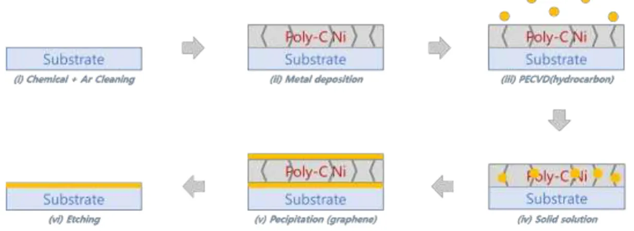
3.1.1 PECVD interfacial graphene growth (LPICM) ... 68
3.1.2 Epitaxial graphene (LPN) ... 70
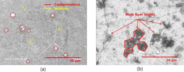
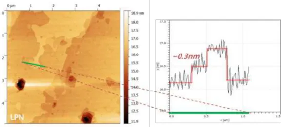
3.2 Graphene Characterization ... 71
3.3 Conclusions ... 73
Reference ... 74
Chapter IV. Electrical Characterization ... 77
4.1 Device fabrication ... 77
4.1.1 Generalities ... 77
4.1.2 Graphene (interaction) on the substrate... 77
4.1.3 Contact electrode deposition ... 78
4.1.3.1 Inkjet printing ... 79
4.1.3.2 Photo-lithography ... 80
4.1.3.3 Shadow-mask metal Evaporation ... 81
4.2 Four-electrode electrical measurements ... 82
4.2.1 Four-probe measurement ... 82
4.2.2 Four-electrode measurement ... 86
4.3 O2, H2O desorption ... 89
4.4 Light exposure response ... 91
4.5 Humidity response ... 95
vii
4.5.2 Vacuum annealing effect ... 97
4.5.3 Surface analysis ... 98
4.5.4 Mechanisms of humidity response ... 101
4.6 Conclusions ... 106
Reference ... 107
Chapter V. Functionalization ... 111
5.1 Generalities ... 111
5.2 Ruthenium Complex(Blue) ... 111
5.3 Functionalization of the device ... 114
5.3.1 Functionalization of the device ... 114
5.3.2 Photoresponse of the functionalized device ... 114
5.4 Double interfaces responses ... 121
5.4.1 Inversed response. ... 126
5.4.1.1 Intensity dependency of the inversed response under vacuum... 126
5.4.1.2 Duty cycle dependency of the inversed response under vacuum ... 128
5.4.2 Charge transfer ... 130
5.5 Conclusions ... 135
Reference ... 136
viii
List of Abbreviation
Acronym
VOCs CG MS CNTs ITO UV LED TFT FET SWIR NIR MIR FIR THz SWF SAW QCM MEMS BAW CVD GO RGO PBSA SEM TEM AFM PESvolatile organic compounds chromatography
mass spectrometry carbon nanotubes indium tin oxide ultraviolet
light emitting diode thin film transistor field-effect transistor short-wave infrared near-infrared mid-infrared far-infrared terahertz
surface work function surface acoustic wave quartz crystal microbalance micro electromechanical systems bulk acoustic wave
chemical vapor deposition graphene oxide
reduced graphene oxide
pyrene butanoic acid succidymidyl ester scanning electron microscopy
transmission electron microscopy atomic force microscopy
ix
Acronym
HOPG GICs SiC FETs CVD SLG PECVD DI UPS ARUPS XPS PMMA UHV IPA MLG SDG MLG PR Id RH AES EELS ECL GO ICMMO MLCTHighly Oriented Pyrolytic Graphite graphite intercalate compounds silicon carbide
field effect transistors chemical vapor deposition single layer graphene plasma enhanced CVD deionized
ultraviolet photoemission
angle-resolved investigation of valence band states X-ray photoemission spectroscopy
polymethyl methacrylate ultra high vacuum isopropyl alcohol multi-layer graphene
single and double layer graphene multi-layer graphene
photo-resist drain current relative humidity
Auger electron spectroscopy electron energy loss spectrum
electrogenerated chemiluminescence graphene oxide
Institut de Chimie Moléculaire et des Matériaux d‟Orsay Metal to Ligand Charge Transfer
1
Résumé en Français
Les progrès récents dans les nanomatériaux présentent un fort potentiel pour la réalisation de capteurs de gaz avec de nombreux avantages tels que: la grande sensibilité de détection de molécule unique, le faible coût et la faible consommation d'énergie. Le graphène, isolé en 2004, est l'un des meilleurs candidats prometteurs pour le développement de futurs nanocapteurs en raison de sa structure à deux dimensions, sa conductivité élevée et sa grande surface spécifique. Chaque atome de la monocouche de graphène peut être considéré comme un atome de surface, capable d'interagir même avec une seule molécule de l'espèce gazeuse ou de vapeur cible, ce qui conduit finalement à un capteur ultrasensible.
Dans cette thèse, un capteur résistif à base de graphène fonctionnalisés a été fabriqué. Le dispositif est basé sur le graphène monocouche sur substrat SiO2 fonctionnalisé avec Ru
complexes(II). Pour comprendre la réponse intrinsèque du film de graphène, un dispositif non fonctionnalisée est d'abord étudié. La réponse du dispositif est sensible à l'environnement de mesure telles que la pression, l'humidité relative et la lumière. Une fois la réponse intrinsèque de l'appareil a été étudié, les dispositifs basés sur le graphène fonctionnalisés ont été fabriqués pour mieux comprendre l'effet de la fonctionnalisation. Deux configurations différentes ont été utilisées; le dispositif fonctionnalisé avec des complexes après le dépôt des électrodes et le dispositif fabriqué en utilisant la surface pré-fonctionnalisé graphène. La réponse de dispositif sous la lumière a été amélioré ou inversé en fonction de sa configuration. Pour élucider ces réponses, les mécanismes du transfert de charge entre les complexes et le dispositif ont été proposées.
Plusieurs types de films de graphène ont été préparés et caractérisés. En LPICM, le graphène est directement synthétisé sur les substrats isolants en utilisant le système de PECVD. Graphène synthétisés par CVD et transférées à SiO2 sont fournis par Thales R & T
tandis que le graphène épitaxiale sur SiC est fourni par LPN. Graphène commercial synthétisé par CVD est également acheté. La plupart des performances des dispositifs à base de graphène dépendent fortement de ses conditions de surface. Afin de minimiser les caractéristiques inattendues provenant de différentes conditions de surface, le graphène monocouche sur substrat SiO2 est finalement choisi en tant que matériau principal utilisé dans
2
La deuxième étape de la fabrication du dispositif est le dépôt des électrodes sur la surface de graphène. Trois approches différentes ont été explorées; jet d'encre d'impression, photo-lithographie et évaporation. En raison de sa complexité et de contaminations possibles à travers le processus, photo-lithographie est exclue. L'impression par jet d'encre promet un processus simple à faible coût, mais le choix limité dans les métaux ne sont pas favorables pour la fabrication de dispositif. L‟évaporation de métal est principalement utilisé comme une méthode de dépôt des électrodes dans ce travail. Avec un masque perforé simple, Ni, Co, Cr / Au, Ni / Au et du Ti / Au électrodes ont été déposés avec succès sur la surface de graphène préparée. L'optimisation des électrodes de dépôt peut être une question intéressante en termes de fabrication du dispositif. Par exemple, la forme et la taille des électrodes et le choix du métal sont des options possibles pour optimiser. Bien que CVD graphène promet la grande surface pour la production de masse de dispositifs, il est polycristallin dans la nature et donc des joints de grains perturbent le transport de charge. En outre, des contaminations de surface à travers le processus sont également préjudiciables au transport de charge du film de graphène. Dans le présent travail, pour faire une moyenne sur ce type de transport limitée défavorable de charge, les électrodes avec 100 μm qui dépasse la taille du grain général de quelques micromètres sont réalisées.
La réponse du dispositif est caractérisé en mesurant la résistance du dispositif. Le concept de la mesure à quatre points est dévelopé pour tenir compte de la forme des électrodes de dispositif et de caractériser le dispositif de façon plus précise. La résistance du dispositif est contrôlée en fonction du temps pour que les changements d'état externes peuvent être directement détectés et interprétés. La réponse du dispositif est simplement exprimé sous la forme des variations de la résistance du dispositif, △R/R0.
La réponse intrinsèque du dispositif est étudié. La réponse du dispositif change lors de l'adsorption / désorption de molécules d'eau et d'oxygène. Désorption de ces molécules sous vide (10-5 mbar) a causé augmentation de plus de 6% en réponse. Ceci est dû à la dé-dopage du film de graphène résultant de l'augmentation de la résistance du dispositif. Désorption des molécules d'eau et d'oxygène peut être en outre accélérée sous l'illumination de la lumière bleue 455 nm avec une intensité de 4 mW/cm2. Dans ce cas, la réponse du dispositif augmente jusqu'à 40%. Étant donné que les résultats montrent que
3
l'adsorption/désorption de molécules d'eau et d'oxygène provoquent des variations sensibles de réponse du dispositif, on peut facilement penser que les changements de réponse de l'appareil lors de la variation relative du niveau d'humidité. A cause du renforcement du dopage par adsorption des molécules d'eau, la réponse du dispositif diminue à mesure que le niveau d'humidité augmente. Cependant, la réponse d'humidité inversée après le recuit sous vide du dispositif à 150 °C pendant 90 minutes. Sur la base des résultats des diverses techniques de PES les mécanismes responsables de deux réponses d'humidité différentes sont proposées. L'adsorption des molécules d'eau sur la surface de graphène et les liaisons hydrogène entre les molécules d'eau et les groupes fonctionnels restants sur le film de graphène sont deux facteurs en compétition responsables de l'élucidation du mécanisme. Les études sur la réponse intrinsèque du dispositif fournissent une compréhension préliminaire pour un capteur de gaz par l‟emploi de graphène. Il convient de noter que les effets de l'air ambiant doivent être pris en compte avant de caractériser le comportement de détection de gaz.
Le capteur résistif sur la base du film de graphène fonctionnalisés avec des [RuII -Pyr]2+ complexe de manière non covalente a été fabriquée. La fonctionnalisation non covalente est appliquée afin d'éviter de modifier les structures électroniques indigènes et de préserver les propriétés intrinsèques du graphène. La réponse du dispositif à la lumière (455 nm) améliorée et rapide a été obtenue qui n‟est pas observables avec un dispositif non-fonctionnalisé. Les électrons transférés des Ru(II) complexes excités aux film de graphène sous la lumière ont amélioré la réponse du dispositif tandis que la photo-désorption de molécules d'eau et d'oxygène adsorbé sur la surface est responsable d'une augmentation lente et globale de la réponse.
L'inversion de la photoréponse a été observée avec un dispositif à double interface qui est fabriqué en déposant quatre électrodes identiques à la surface de graphène pré-fonctionnalisée. La première interface est entre la couche d'adhérence de l'électrode métallique et le Ru(II) complexe tandis que la seconde interface est entre le Ru(II) complexe et le graphène. Le mécanisme proposé responsable de l'inversion de la réponse est basée sur les variations de l'orientation des flux de transfert de charges. Au début, les électrons sont transférés de Ru(II) complexes excités à graphène alors qu'ils se sont rendus à vers la couche
4
oxydée d'adhérence après la mesure continue et répété sous la lumière.
Pour conclure, les approches théoriques et expérimentales et les résultats obtenus au cours de cette thèse ouvrent un moyen de comprendre et de fabriquer le futur captuer de gaz par l‟emploi de graphène fonctionnalisé de façon non covalente.
5
Chapter I
Introduction
Chapter I.Introduction ... 6
1.1 Overview ... 6
1.2 Graphene: Carbon allotropes, Properties and Applications ... 9
1.2.1 Carbon Allotropes ... 9
1.2.2 Graphene properties ... 10
1.2.2.1 Electronic band structure of graphene ... 10
1.2.2.2 Electrical Properties ... 14
1.2.3 Graphene for device applications ... 15
1.2.3.1 Graphene based electrode ... 15
1.2.3.2 Graphene based transistor ... 16
1.2.3.3 Graphene for Battery ... 16
1.2.3.4 Graphene for photonic devices ... 17
1.2.3.5 Graphene for gas sensing applications... 18
1.3 Functionalized graphene ... 23
1.3.1 Covalent functionalization ... 23
1.3.2 Non-covalent functionalization ... 24
1.4 Conclusions ... 27
6
Chapter I.Introduction
1.1 Overview
The modern advanced technology and the global development of industrial activities has been accompanied by a variety of serious environmental problems. One example is the release of various chemical pollutants such as NOx, SOx, COx and volatile organic
compounds (VOCs) into the atmosphere caused from various manufacturing industries and fossil fuel consumption of private sectors resulting in global environmental air pollution.
Air pollution can cause severe problems related to human health and environment. It can simply cause, for example, a disease like asthma. Asthma is a disease affecting the airways that carry air to and from the lungs. It is estimated that the total cost of asthma in Europe is 19.3 billion euros per annum [1]. Another example of the consequence of air pollution is acid rain. Any industrial and private activities resulting in the emissions of nitric and (NOx) sulfuric acids (SOx) are responsible for acid rain. It usually erodes buildings and
affects human health through the contamination of water and harmed vegetation [2].
In addition to air pollution, the release of combustible gases such as methane, ethane, butane, hydrogen and acetylene can also constitute significant risks in terms of possible explosions of plants [3,4]. This sort of industrial accident not only leaves industrial damages but also threats civil security.
To minimize the above stated damages, the development of new sensing platforms and technologies to be used in real world for detecting and quantifying environmental pollution, especially toxic and combustible gases are required [5]. Optical spectroscopy and gas chromatography/mass spectrometry (CG/MS) are well-known analytic instruments that have been widely used for air pollutant measurements. Although these instruments can give a precise analysis, they are time-consuming, expensive, and can seldom be used in real-time in the field. Gas sensors that are compact, robust, with versatile applications and a low cost are needed. To meet this demand, considerable research into new sensors is underway, including efforts to enhance the performance of traditional devices, such as gas sensors based on semiconductor (Si) structures [6,7]. Numerous materials have been reported to be usable as semiconductor sensors including both single- (e.g., ZnO, SnO2, WO3, TiO2 and Fe2O3) and
7
multi-component oxides (BiFeO3, MgAl2O4, SrTiO3, and Srl-yCayFeO3-x) [8]. Such devices
were applied to detect hydrogen [6,7], oxygen [9,10], carbon monoxide [9,10], hydrogen sulfide [11], or as active element of smoke detectors [12]. However, this type of sensors are generally limited by their high operating temperature (150-600 ˚C).
Recent advances in nanomaterials provided a strong potential to create a gas sensor with many advantages including a very high sensitivity down to single molecule detection, low cost, and low power consumption. This is well reflected by the fact that nanosensor arrays are already under development by giant firms such as Dow Corning, Samsung, Boeing, Lockheed Martin, IBM, and Agilent. Among nanomaterials, graphene that was first isolated in 2004 [13], is one of the best promising candidate for the future development of nanosensors applications because of its atom-thick, two-dimensional structures, high conductivity, and large specific surface areas [14-18]. Every atom of a monolayer graphene can be considered as a surface atom, capable of interacting even with a single molecule of the target gas or vapor species, which eventually results in an ultrasensitive sensor response. The potential advantages of graphene based sensor, in short, are that it can be ultra-compact, effective at room temperature, characterized by low-power consumption, low cost, high sensitivity, selectivity and with a very low response and recovery time.
However, despite its great potential abilities as a sensing material, graphene still face some difficulties to be overcame for development of its practical use in sensing applications such as large area homogeneous production, contacting and devices integration, selective sensing mechanisms and so on. Since its discovery, there have been many efforts to improve its quality and to synthesize large area homogeneous layer [77,81,90] and more, recently, there are also many trials to functionalize graphene with various elements to improve its sensitivity, specificity, solubility, loading capacity, etc [97-104]. Keeping step with this tendency, this thesis tries to further develop the graphene based gas sensor by non-covalent functionalization of its surface. The main purpose of functionalizing the surface of graphene is to improve its specificity for selective sensing of the device. We have tried to reach this objective by exploring functionalization of graphene via an organometallic complex. Such approach can allow (via appropriate choice of the functionalizing complex) to each type of gas to interact in a specific way with each metal, changing in a specific way the graphene
8
resistivity thus acting as fingerprinting for identifying the targeted gases.
The following chapters will describe the development of our graphene based gas sensor. In Chapter 1, after this overview, we review the fundamental properties and various applications of graphene. The preparation methods of graphene are then stated in Chapter 2 followed by the introduction of various graphene layer characterization techniques. In Chapter 3, graphene layers used in our experiments are introduced with their preparation and characterization. Chapter 4 explains the theoretical backgrounds of the electrical characterization of our device in details with obtained experimental results. Chapter 5 describes the functionalization methods utilized in our experiment and the experimental results obtained from functionalized graphene based device. The conclusion summarizes this thesis and give an outlook for graphene based sensor.
9
1.2 Graphene: Carbon allotropes, Properties and Applications
1.2.1 Carbon Allotropes
Graphite, whose name stems from the Greek word “graphein” meaning to draw or write, is now losing his authority in regard of writing and documentation. Times have changed and the manner of writing and keeping documents has been changed as well. Today, it seems even more natural to type a letter looking at the computer monitor rather than to write it traditionally on the paper holding a pencil. On the other hand, given their exceptional physical and electrical properties, graphene and carbon nanotubes (CNTs) have been trying to take back so-called carbon allotropes‟ authority in various scientific fields in recent years.
Carbon exists in several forms called allotropes and diamond is one of them with a very strong crystal lattice. Graphite is another well-known carbon allotrope in which the graphene layers are stacked to form 3D structure. In 1985, another allotrope called fullerenes(C60) was discovered by Kroto et al [19]. Its structural closed ball shape guides us
to the 0-dimensional electronics. In 1991, CNTs were observed by Iijima‟s group [20]. As its name suggests, CNTs are made of rolled up graphene layers forming 1-dimensional tube structure. The individual graphene layer, a 2-dimensional flat layer of carbon atoms highly packed into honeycomb lattice and is a building block of the other allotropes as shown in the (Figure 1.1.), was first isolated by Manchester group [13] in 2004.
10 1.2.2 Graphene properties
Since its discovery, graphene has been an appealing and attractive material for many researchers due to its exceptional properties. It is optically transparent (~97.7% transparency for visible light) [21], mechanically robust (Young‟s modulus of 1.0TPa and stiffness of 130 GPa) [22] and it has high thermal conductivity (~6,000 W/mK) [22] as well. The attractiveness becomes even amplified when it comes to its excellent electrical properties. Theoretically, it has extremely high charge mobility (~200,000 cm2/Vs) at room temperature which is about 200 times higher than that of Si. A very low resistivity (10-6 Ωcm), even less than that of silver, was observed for the suspended graphene as well [23]. It can also carry high current density up to 3x10⁸ A/cm2 [24]. The origin of such unique properties of graphene will be explained by understanding its electronic band structure.
1.2.2.1 Electronic band structure of graphene
As its atomic number on the periodic table implies, carbon has 6 electrons. Then the ground-state electron configuration of carbon atom can be represented as 1s2
2s22p2 where 2 electrons are filling the inner shell while the other 4 are occupying outer shell. The combination of one 2s atomic orbital and two 2p atomic orbitals forms three equivalent sp2
hybrid orbitals and carbon atoms use this sp2 hybrid orbitals to form covalent bonds with each other when they are constructing graphitic materials like graphite, graphene and CNTs (Figure 1.2.). Three sp2 hybrid orbitals lie in a plane and the angle between them is 120° while the third 2p atomic orbital consists of two lobes lying perpendicular to that plane.
In graphene, the overlap of these sp2 hybrid orbitals in plane forms the sigma(σ)
bond between the carbons atoms leading to the honeycomb lattice formation while remaining 2p orbitals on adjacent carbon atoms perpendicular to the plane overlap to form delocalized pi(π) bond. Since they are much closer to the Fermi surface than σ electrons, π electrons are responsible for charge carrier transport of graphene and determine the electronic properties of graphene at low energy.
11
Figure 1.2. (a) Hybridized three sp2 orbitals for a carbon atom and (b) an unhybridized 2p orbital
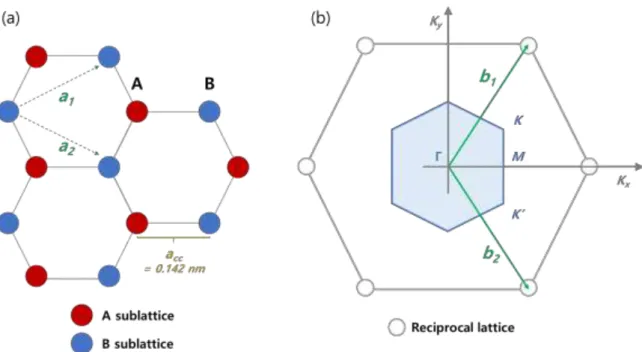
Figure 1.3. shows the typical honeycomb lattice of graphene with unit vectors in real space and the reciprocal lattice space. The distance between two nearest carbon atoms acc is
estimated to be 0.142 nm [25]. As shown in the Figure 1.3.(a), the honeycomb lattice in real space can be expressed with two sub lattices A and B of the triangular Bravais lattices [26]. Based on the Figure 1.3.(a), the unit cell vectors a1 and a2 can be expressed as
( √ ) ( √ ) (1)
where acc = 0.142 nm is the distance between two nearest carbon atoms [25].
Corresponding reciprocal lattice vectors b1 and b2 can then be express as
( √ ) ( √ ) (2)
For deriving electronic band structure of graphene can be we account the reciprocal lattice of the triangular lattice. The shaded region in the Figure 1.3.(b) is the first Brillouin zone (BZ) of graphene where Gamma point (Γ) corresponds to its center while K points on its corners represent Dirac points.
12
Figure 1.3. (a) Schematic of honeycomb lattice of graphene with the unit vectors a1 and a2.
(b) Reciprocal lattice with Brillouin zone (BZ) where b1 and b2 are the reciprocal vectors.
In 1947, the first tight-binding model of graphene was reported by Wallace [27] concerning the nearest and next-nearest neighbor interactions for 2p orbitals. Saito et al. in 1998 reported advanced tight binding approximation by expanding conventional model with the wave function overlap of different atoms [28]. Based on their calculation that takes only the nearest neighbor interactions into account, the energy dispersion relation in graphene can be obtained
( ) √ √ (3)
where denotes the transfer integral between nearest neighbor so that the energy has the values of , and 0 at the high symmetry points, Γ, M and K in the BZ respectively.
Energy dispersion of graphene can be visualized by plotting above equation. Figure 1.4.(a) represents the energy as a function of wave vectors produced by MATLAB with
13
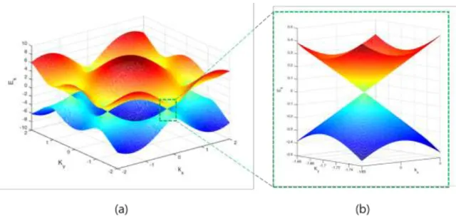
=2.8 eV and the lattice constant, √ . As we can see, conduction band and valence band are touching at Dirac points which is well consistent with the zero energy value calculated at K points. At these Dirac points, intrinsic graphene can be considered as a zero band gap semiconductor with the linear energy dispersion relation (Figure 1.4.(b)). Such linear dispersion relation near these Dirac points provides most of interesting electronic properties of graphene and it can be described as
( ) | | (4)
where is the wave vector and (~106 ms-1) is the Fermi velocity. The effective mass depends on the second derivative of the energy with respect to the wave vector . It becomes zero for this linear dispersion relation. Hence, electrons in graphene have zero effective mass. They behave like massless Dirac fermions with the speed of , at the K and K‟ points in BZ. This explains why they are called the Dirac points.
14 1.2.2.2 Electrical Properties
As the Fermi level in the intrinsic graphene is located at the Dirac point where the density of states becomes zero, theoretically the electrical conductivity of intrinsic graphene has to be very low. On the other hand, depending on the Fermi level changes, graphene can easily be either n-doped or p-doped having quite high electrical conductivity. It can be doped by several ways among which applying an electric field. Figure 1.5. is showing the ambipolar electric field effect in monolayer graphene [29] which is the clear evidence of alternating doping state of graphene by the Fermi level changes.
Figure 1.5. Ambipolar electric field effect in monolayer graphene [29]
Adsorption of water or other gas molecules on its surface can also induce graphene doping. This is one of the most important features of graphene for sensing applications and it will be discussed in details in the following chapter. It is also reported that the structural defects like vacancy in graphene increases the material conductivity, while the remaining functional groups through the synthesis process might work as carrier scattering centers and effectively reduce charge mobility.
Researchers working on graphene have extensively studied and reported its electrical properties. It has extremely high charge mobility (~200,000 cm2/Vs) at room temperature which is about 200 times higher than that of Si. This high charge mobility value is observed for the suspended graphene with the carrier density of about 1012/cm2 and a corresponding
15
resistivity of about 10-6 Ωcm [23] which is even less than that of silver.
However, when graphene sits on a SiO2 substrate, for example, for the device
fabrication applications, its mobility can be strongly limited via the substrate optical phonon scattering and the typical reported values are about 40,000 cm2/Vs at room temperature [30,31] that is 5 times less than that of suspended graphene.
1.2.3 Graphene for device applications
Thanks to its excellent electrical properties combined with optical (~97.7% transparency for visible light) [21], mechanical (Young‟s modulus of 1.0TPa and stiffness of 130 GPa) [22] and thermal properties (6,000 W/mk) [22], graphene has received great attention as one of the most promising candidates for the future development of various nanodevices. In the following, we introduce several graphene based devices that are being studied by many researchers.
1.2.3.1 Graphene based electrode
Since it has high surface to mass ratio and excellent conductivity with relatively low sheet resistance (~300 Ω/sq) [32,33] (Figure 1.6.(a)), graphene becomes a promising candidate for use as an electrode. Due to its transparency (~97.7% for single layer graphene) [21], it is further predicted to be a good candidate for a next transparent conducting film (TCF) replacing indium tin oxide (ITO). ITO has been most actively used as a transparent electrode, mainly in display and solar cell industry. However, because of the limited supply of indium, the cost of ITO is continuously increasing [34]. Furthermore, the transmittance of ITO rapidly drops above visible light wavelength which might limit its use for ultraviolet (UV) sensors and light emitting diode (LED); for this spectral region, graphene transmittance stays stable at around 97.7 % for single layer graphene [35] (Figure 1.6.(b)).
16
Figure 1.6 (a) Sheet resistance and (b) transmittance of transparent conducting films: ITO, single layer graphene and single wall carbon nanotube [35]
1.2.3.2 Graphene based transistor
Due to the excellent electrical properties detailed above, graphene is considered to be the future material which may replace conventional Si based electronics. One example is the graphene based thin film transistor (TFT). Even though the zero band-gap features of graphene limits its use in digital applications, the high carrier mobility enables graphene to be used for high frequency devices [33,36,37]. Graphene based TFT also features high current density (~2x10⁸A/cm2) [38] and high saturation velocity (~5x107cm/s) [39] which become more important measure of the transport properties [40] for miniaturized micro/nano devices. However, the quality control and the scalability of synthesized graphene still remain as an obstacle to overcome.
1.2.3.3 Graphene for Battery
There have been huge improvements of portable electronic devices in recent few years and thereby equivalent improvements in rechargeable solid-state batteries are being demanded. Today, the battery industry is dominated by lithium-ion technology which enable flexible and light weight design with high energy density. Currently carbon materials such as disordered carbon [41,42] and acid treated graphite [43] are widely used in lithium batteries
17
while carbon nanotube (CNT) is being most actively studied as an electrode due to its unique structural property that enables rapid insertion/removal of lithium ions [44,45]. Meanwhile, the major interests of the advanced battery research deal with the fabrication of flexible batteries that could be compatible with wearable electronic devices. CNTs are often considered as a good candidate for such flexible electronics. However, practical application as battery electrodes are limited by the relatively high production cost and the difficulties in producing homogeneous and stable CNT sheets [46,47]. On the contrary, graphene may assure a lower production cost with appropriate synthesis and processing methods. Furthermore, taking account of a number of graphene sheets, the specific storage capacity of graphene may correspond either to 780 mAh/g or to 1,116 mAh/g [48,49,50] depending on different interaction descriptions between graphene and lithium; these values exceed the capacity of graphite (372 mAh/g) [51] and are comparable to that of CNT (1,100 mAh/g) [52].
1.2.3.4 Graphene for photonic devices
Graphene is also an appealing material for photonic devices mainly due to its previously stated exceptional optical and electrical properties. Among many photonic devices, graphene based photodetector is most actively investigated for several reasons. First of all, graphene is a zero band gap material. Hence, photoelectrons can be generated by light absorption over a wide range of optical energy spectrum which is not probable with conventional semiconductors such as Si and InGaAs. The maximum detectable light wavelength for Si and InGaAs ends at ~1,100 nm and 2,600 nm respectively [53] while graphene covers wider ranges of practical light wavelength including ultraviolet, visible, short-wave infrared (SWIR), near-infrared (NIR), mid-infrared (MIR), far-infrared (FIR) and terahertz (THz) spectral regimes as well [54]. Besides, we might also benefit from its ultrafast carrier dynamics [55,56], wavelength-independent absorption [57-59], tunable optical properties by electrostatic doping [60,61] and high carrier mobility that enables ultrafast operation of graphene based photodetectors [62-65]. In addition to the photodetector, many efforts have been devoted to employing graphene for the development on an optical modulator [61,66,67], optical polarization controller [68,69] or mode-locked laser/Thz generator [70,71].
18 1.2.3.5 Graphene for gas sensing applications
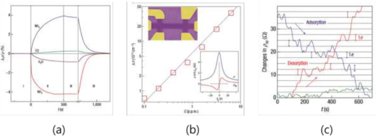
To the best of our knowledge, it is known that the very first reported gas sensor based on graphene was fabricated by F.Schedin et al[72] in 2007. Mechanically exfoliated graphene was used as an active layer of field-effect transistor (FET) and the device was fabricated on the silicon wafer with 300 nm SiO2 layer. The device was made as a hall bar geometry so as
to measure both longitudinal and transverse resistivity under applied magnetic field where one can directly calculate the charge carrier concentration changes. Various gases such as NH3, CO, H2O and NO2 were diluted to 1 ppm and tested. Figure 1.7.(a) shows the result
where NH3 and CO were found to act as electron donners while H2O and NO2 acted as
acceptors. The authors also reported that carrier concentration depends linearly on the relative gas concentration (Figure 1.7.(b)). The quantized sensor response represented by the step-like changes in Hall resistivity near the neutrality point (|n|<1011cm-2) during adsorption and desorption of strongly diluted NO2 (Figure 1.7.(c)) clearly suggests evidence for individual
adsorption and desorption phenomena as well.
Figure 1.7. Sensitivity of graphene to chemical doping (a) changes in resistivity at zero B
upon exposure to various gases. (b) linear dependence between carrier concentration and gas concentration. (c) Single-molecule detection of strongly diluted NO2.
The detection mechanism of most of graphene based gas sensors, as demonstrated by above introduced device, is mainly based on the changes in electrical conductivity of the graphene layer. Adsorption and desorption of target gas molecules can act either as donors or
19
acceptors thus modifying the carrier density or the mobility and resulting in the conductance changes. In addition to this simple and direct measurable detection mechanism, graphene has many other advantages in regards of potential gas sensing applications:
Large theoretical specific surface area (~2600 m2/g) [22] that provides high surface-to-volume ratio where every atom can be considered as surface atom interacting with a single target gas molecule
Exceptional electronic properties of graphene make it possible to have fast response. Besides, being a zero gap semiconductor, graphene can detect even a small change in charge carriers caused by subtle adsorption and desorption process.
Inherently low flicker [73] and Johnson noise [72] that enable graphene based sensors to have very large signal-to-noise ratio at room temperatures.
Conventional thin film electronic engineering and processing techniques are compatible with graphene. Hence, graphene based devices such as four-terminal resistor and FET are relatively easy to fabricate.
By avoiding expensive lithography process, low-cost graphene based gas sensor can be fabricated for certain device configurations such as four-terminal graphene resistor.
Further progress on a synthesis of large-area graphene by chemical vapor deposition (CVD) process may enable mass production of graphene based gas sensor which may be an important issue from industrial and practical point of view [74,75].
Graphene is 2-D material but it shares most of the CNTs technology advantages; most of surface chemical treatments which are already verified with CNTs are applicable to graphene as well.
With all these great advantages for gas sensing applications development, many researchers have already reported various types of graphene based gas sensors in different device configurations including resistive, FET, surface work function (SWF) transistors, surface acoustic wave (SAW) sensor, quartz crystal microbalance (QCM) sensor, micro electromechanical systems (MEMS) and metal oxide hybrid gas sensors and so on. Most of
20
reported solid state gas sensors so far adopt resistor/FET configurations because of its maturity in technological understanding.
For the resistive graphene based gas sensors, device resistance changes induced by adsorbed gas molecules are measured. Simple fabrication and direct measurements are the great advantages [76-78] of this type of sensors. On the other hand, for the graphene based FETs, the measured drain current upon exposure to the target gases can either be affected by the applied gate bias or by the adsorption of gas molecules. In this case, the performances of sensors strongly depend on the on/off ratio where a higher sensitivity requires a higher on/off ratio [79,80]. SWF transistor sensor is another type of transistor based graphene gas sensor. The adsorption of target gas molecules changes its surface dipole moment and its electron affinity and thereby increase the surface work function of graphene [81]. The detection mechanism of SAW sensors is based on the frequency response of graphene layers caused by either mass changes or conductance changes resulting from the adsorption/desorption of target gases [82]. QCM is one of the most popular bulk acoustic wave (BAW) sensors where the frequency response is interpreted mass changes depending on adsorption/desorption of target gas molecules [83]. Recently, advanced MEMS technology are employed in order to make the best use of graphene films as sensing material on micro/nano devices [84] as well. This miniaturization of sensors benefits from many advantages such as high sensitivity with fast response, low temperature operation, low power consumption, and low cost mass production [85]. Meanwhile, there were even some efforts to fabricate hybrid gas sensors that combine the advantages of graphene based gas sensors with those of conventional semiconducting metal oxides [86-89].
For sensing applications, the sensitivity of the device is one of the most important device characteristics. Like all other materials used as active layer for solid state sensors, for graphene based gas sensors, the sensitivity relies very much on the nature of graphene layer. The ideal graphene is a perfect crystalline structure with infinite surface area which has no dangling bonds on its surface that are required for the adsorption of gas molecules. Such a perfect graphene can be obtained via mechanical exfoliation but its size is limited to a few micrometers and the method has low throughput. On the other hand, graphene synthesized by chemical vapor deposition (CVD) process can produce large surface area films which
21
promises high throughput for device applications. However, because of the imperfection of synthesis process, CVD graphene is generally produced with some defects which are considered to be important for gas sensing applications [90,91]. Masel et al [92] in 2012 has reported that the type and geometry of graphene defects affect the sensitivity of a graphene based gas sensor. For example, the Figure 1.8. clearly shows that the device based on defective graphene has higher sensitivity compared to the pristine graphene based device. The gas sensor with pristine graphene has shown almost negligible response while that with intentionally introduced line defects on the graphene surface has shown up to 6% conductance increase. As the line defects extended to finally cut the graphene sheet into ribbons with width in the range of several micrometers, the device response further increases by two times over that of line defects device, or up to 12% conductance increase.
Figure 1.8. Response of the pristine and defective CVD-graphene to 1,2-dicholorobenzene. [92]
In addition to this study, many researchers reported that the sensitivity of graphene can also be effectively enhanced by functionalizing it with polymers, metals or other surface modifiers [93-96]. Likewise, the device sensitivity might change significantly depending on the nature of the graphene layer. However, unexpected an poorly known defects can be produced at any process steps including synthesis, transfer, electrode deposition and so on. Hence, graphene should be carefully characterized from the first synthesis process step to the final device fabrication in order to understand and manage fabricated devices behavior in terms of its sensitivity.
22
The second important device characteristics for sensing applications would be the specificity. The sensitivity of graphene based gas sensor for a certain gas molecule might be comparable to that obtained for a range of different gas species and mixtures. Hence, definitive identification of detected gas molecules is not easy. For example, when the graphene based sensor is exposed to the mixture of NO2 and NH3 gas molecules, the former
increases device conductance while the latter reduces it. Then the combination of these two opposite effects may result in almost zero device response misleadingly representing zero gas molecule detection which is not the case. Moreover, it is also possible to mix different gases in various relative concentrations in order to yield the same net device response. Therefore, it is necessary to develop approaches allowing graphene based devices to detect only the target gas molecules. Probably one of the most effective way to realize this specificity in graphene based gas sensor is to functionalize graphene layer with certain elements that react only with certain gas molecules.
23
1.3 Functionalized graphene
Despite its great potentialities in device applications, as a zero gap and inert material, ideal graphene sometimes loses its competitiveness in the field of semiconductors and sensors. To this respect, graphene is often functionalized with various elements for many purposes such as improvement of sensitivity, specificity, solubility, loading capacity, etc [97-104]. For gas sensing applications, improved sensitivity and specificity may be the main purposes of functionalization. Fortunately, various strategies have already been devised for functionalizing CNTs based devices and these approaches are compatible with graphene as well [105]. Following sections will briefly introduce the two main functionalization ways: covalent and non-covalent functionalization.
1.3.1 Covalent functionalization
The covalent functionalization of pristine graphene surface with organic functional groups has been developed for several purposes. The main purpose is to improve graphene dispersion in common organic solvents [106]. For example, oxygen containing functional groups such as carboxylic(-COOH), hydroxyl(-OH), usually found in graphene oxide (GO) or reduced graphene oxide (RGO), can be covalently bound on the surface of graphene by using strong acids [106]. Graphene can easily be fluorinated and several chemical functional groups such as amino, hydroxyl or alkyl groups can also form covalent bond with carbon atoms by replacing those fluorine atoms [107-109]. Sometimes, covalent functionalization can also be used to serve as an amplification mechanism for further functionalization of sensing probes or as a spacing between graphene and sensing probes [110]. For the covalent functionalization, functional groups are firmly bound by forming covalent bonds and ensure their proper functions on the graphene surface. However, it is well known that the covalent bonds convert sp2 carbon bonds to sp3 carbon bonds. This will than create electron scattering centers that will limit the performances of the devices by altering native electronic structure and physical properties of graphene.
24 1.3.2 Non-covalent functionalization
Non-covalent functionalization is often employed to avoid altering the pristine electronic structures of graphene and thus preserve its intrinsic properties. Functional molecules can be grafted onto graphene by the aid of linkers. One of the most frequently used linkers is the pyrene moiety. It has been reported to have a strong affinity toward graphene surface via strong π-π interaction [111,112]. For example, Xu et al. prepared stable aqueous dispersions of graphene flakes by functionalizing graphene oxide with pyrenebutyric acid [113]. Wang et al., on the other hand, has employed non-covalently functionalized graphene with pyrene butanoic acid succidymidyl ester (PBSA) rather than pristine graphene to improve the power conversion efficiency of organic solar cell devices. The π-π interaction between graphene and PBSA has negligible effect on the optical absorption of visible light of graphene layer. They have reported functionalized graphene improvement up to 1.5 % of the power conversion efficiency compared to that with pristine graphene [114] (Figure 1.9.).
An et al. have also reported versatile hybrid film based on the non-covalently functionalized graphene films with 1-pyrenecarboxylic acid (PCA) [115]. They laminated PCA functionalized graphene film onto flexible and transparent polydimethylsiloxane (PDMS) layer. This hybrid film shows differentiated optical and molecular sensing properties compared with pristine graphene film while its conducting nature remains the same. It blocks 70 to 95 % of UV light and passes more than 65 % of visible light. Besides, the electrical resistance was found to be also changing upon the visible light illumination, the pressure changes, and the exposure to different types of gas molecules. This multi-functionality of the film promises its future applications in various fields. Other bifunctional complexes having a reactive end and an aromatic tail such as thionine, perylene tetracarbonxylic acid and porphyrin derivatives are used as linkers for non-covalent functionalization as well [116].
25
Figure 1.9. (a) Schematic view and energy diagram of the organic solar cell fabricated with graphene. (b-e) I-V characteristics of the solar cell devices based on graphene films in the dark and under illumination: (b) pristine graphene, (c) UV treated graphene, (d) graphene functionalized with PBSA and (e) ITO for the comparison. [114]
On the other hand, graphene can be considered as an ideal substrate for the dispersion of nanoparticles due to its large specific surface area (~2600 m2/g) [22] compared to that of CNTs, amorphous carbon or graphite. Furthermore, graphene is free of metallic or carbon impurities which is not the case for CNTs. Many researchers have already reported
26
graphene films decorated with metal nanoparticles (e.g., Au, Ag, Pt, Rh, Pd) in a variety of applications such as fuel cells, sensors, supercapacitors, and batteries [117-122]. In addition, due to the fact that GO and RGO surface contains oxygen containing functional groups, they are often employed for the nanoparticle decoration as well. This decoration is done in non-covalent way such as reduction process [123,124], electrospray [125] or electrochemical deposition [126].
27
1.4 Conclusions
Since its discovery, graphene has been an appealing and attractive material for many researchers due to its exceptional properties originating from its unique linear energy-momentum dispersion. For example, it is optically transparent (~97.7 % transparency for visible light), mechanically robust (Young‟s modulus of 1.0 TPa and stiffness of 130 GPa) and has high thermal conductivity (6,000 W/mK), high theoretical charge mobility (~200,000 cm2/Vs) at room temperature and low resistivity (10-6 Ωcm).
Thanks to its excellent physical properties, graphene has received great attention as one of the most promising candidates for the future development of various nanodevices. It is a promising alternative as a next TCF replacing ITO. Graphene based TFT is another promising device, but the quality control and the scalability of synthesized graphene still remain as an obstacle to overcome. It is also used in the advanced battery research dealing with flexible electronic devices. Many efforts have been devoted to employing graphene for the development of photonic devices, such as optical modulator, optical polarization controller, mode-locked laser/THz generator and photodetector. Graphene based gas sensor
Despite its great potentialities in device applications, as a zero gap and inert material, ideal graphene sometimes loses its competitiveness in the field of semiconductors and sensors. To this respect, graphene is often functionalized with various elements for many purposes such as improvement of sensitivity, specificity, solubility, loading capacity, etc. Graphene can be either covalently or non-covalently functionalized. However, covalent bonds convert sp2
carbon bonds to sp3 carbon bonds thus limit the performances of the device by altering
electronic structure and physical properties of graphene. On the other hand, non-covalent functionalization is often employed to preserve intrinsic graphene properties while keeping advantages resulting from the functionalization.
Current environmental problems including air pollution via the release of chemical pollutants originating from the modern advanced technology and the global development of industrial activities are threatening human health. To prevent such problems, the development of new sensors that are compact, robust, with versatile applications and a low cost is needed. In this regard, graphene based sensor is one of the best promising candidate that provides
28
various potential advantages: ultra-compact, effective at room temperature, low-power consumption, low cost, high sensitivity, selectivity, low response and recovery time. Furthermore, graphene can be non-covalently functionalized to improve its specificity for selective sensing of the device.
29
References
[1] European Respiratory Society White Book, 2012
[2] Johnson, D.W. and S.E. Lindberg, Atmospheric deposition and forest nutrient cycling. A synthesis of the Integrated Forest Study. 1992: Springer-Verlag.
[3] Susott, R.A., Characterization of the thermal properties of forest fuels by combustible gas analysis. Forest Science, 1982. 28(2): p. 404-420.
[4] Yamazoe, N. and T. Seiyama, Sensing mechanism of oxide semiconductor gas sensors. IEEE CH2127, 1985. 9: p.376-379
[5] Jing Kong, Nathan R. Franklin, Chongwu Zhou, Michael G. Chapline, Shu Peng, Kyeongjae Cho, Hongjie Dai, Nanotube Molecular Wires as Chemical Sensors, Science, 28 jan 2000, Vol. 287, Issue 5453, pp. 622-625.
[6] K.I.Lundstrom, M.S.Shivaraman, C.M.Svensson, and L.Lundkvist, A hydrogensensitive MOS field-effect transistor, Appl. Phys. Lett. 26 (1975) 55-57.
[7] Geyu Lu, Norio Miura, Noboru Yamazoe, High-temperature hydrogen sensor based on stabilized zirconia and a metal oxide electrode, Sensors and Actuators B 35-36 (1996) 130-135
[8] B.Hoffheins, Solid State, Resistive Gas Sensors, in Handbook of Chemical and Biological Sensors, R.F. Taylor and J.S.Schultz, eds., Philadelphia: Institute of Physics, 1996.
[9] W.P.Kang, and C.K.Kim, Novel platinum-tin-oxide-silicon nitride-silicon dioxide-silicon gas sensing component for oxygen and carbon monoxide gases at low temperature, Appl. Phys. Lett. 63 (1993) 421-423.
[10] W.P.Kang, and C.K.Kim, Performance and detectionmechanism of a new class of catalyst(Pd,Pt, or Ag)-adsorptive oxide (SnOx or ZnO)-insulator-semiconductor gas sensors, Sensors and Actuators B 22(1994) 47-55.
[11] S.Shivaraman, Detection of H2S with pd gate MOSFETs, J.Appl. Phys. 47 (1976) 3592-3593.
30
[12] I.Lundstom, S.Shivaraman, L.Stiblert, and C.Svenson, Hydrogen in Smoke detected by the palladium-gat-field-effect transistor”, Rev.Sci.Instrum. 47(1976) 738-740.
[13] Novoselov, K.S., Gim, A.K., Morozov, S.V., Jian, D., Zhang, Y., Dubonos, S.V., Grigorieva, I.V. and Firsov, A.A. Electric field effect in atomically thin carbon films. Science 306, 666-669 (2004)
[14] M.Pumera, A. Ambrosi, A.Bonanni, E.L.K.Chang, H.L.Poh, Graphene for electrochemical sensing and biosensing, Trends in Analytical Chemistry 29(2010) 954-965. [15] Y.H.Wu, T.Yu, Z..Shen, Two-dimensional carbon nanostructures: fundamental properties, synthesis, characterization, and potential applications, Journal of Applied Physics 108 (2010) 071301-0713039.
[16] C.Soldano, A.Mahmood, E.Dujardin, Production, peroperties and potential of graphene, Carbon 48 (2010) 2127-2150.
[17] E.Massera, V.L.Ferrara, M.Miglietta, T.Polichetti, I.Nasti, G.Francia, Gas sensors based on graphene, Chemistry Today 29 (2010) 39-41.
[18] R.Arsat, M.Breedon, M.Shafiei, P.G.Spizziri, S.Gilje, R.B.Kaner, K.Kalantar-zadeh, Chemical Physics Letters 467 (2009) 344-347.
[19] Kroto,H.W., Heath, J.R., O‟Brien, S.C., Curl, R.F. and Smalley, R.E, C60: Buckminsterfullerene, Nature 318, 162-163 (1985)
[20] Iijima, S.Helical, Microtubules of graphitic carbon, Nature 354, 56-58 (1991)
[21] R.R.Nair, P.Blake, A.N.Grigorenko, K.S.Novoselov, T.J.Booth, T.Stauber, N.M.R.Peres, A.K.Geim, Fine Structure Constant Defines Visual Transparency of Graphene, Science 06 Jun 2008, Vol.320, Issue 5881, pp.1308
[22] Zhu,Y., Murali,S., Cai,W., Li,X.,Suk,J.W., Potts, J.R. and Ruoff, R.S., Graphene and Graphene Oxide: Synthesis, Properties, and Applications, Advanced Materials 22, 3906-3924 (2010)
31
J.A.andGeim, A.K., Giant Intrinsic Carrier Mobilities in Graphene and Its Bilayer., Physical Review Letters 100, 016602 (2008)
[24] Moser, J., Barreiro, A. and Bachtold, A. Current-induced cleaning of graphene, Applied Physics Letters 91, 163513-3 (2007).
[25] J-T. Wang, C.Chen, and Y.Kawazoe, New carbon allotropes with helical chains of complementary chirality connected by ethane-type π conjugation., Sci.Rep., vol.3, p.3077, Jan. 2013.
[26] F.Jean-Noel and G.Mark Oliver, Introduction to the Physical Properties of Graphene, 2008.
[27] Wallace, P.R. The Band Theory of Graphite. Physical Review 71, 622-634 (1947).
[28] R.Saito, G.Dresselhaus, and M.S.Dresselhaus, Physical Properties of Carbon Nanotubes (Imperial, London, 1998).
[29] A.K.Geim, K.S.Novoselov, The rise of graphene, Nature Materials, 6, 183-192 (2007) [30] M.F.Cranciun, S.Russo, M.Yamamoto, S.Tarucha, Tuneable electronic properties in graphene, Nano Today 6 (2011) 42-60
[31] C.Daniela, V.D.Marcano, J.M.Kosynkin, J.M.Berlin, A.Sinitskii, Z.Sun, A.Slesarev, L.B.Alemany, W.Lu,M.J.M.Tour, Improved synthesis of graphene oxide, ACS Nano 4 (2010) 4806-4814
[32] Pang, S., et al., Graphene as Transparent Electrode Material for Organic Electronics. Advanced Materials, 2011. 23(25): p.2779-2795.
[33] De, S. and J.N. Coleman, Are There Fundamental Limitations on the Sheet Resistance and Transmittance of Thin Graphene Films? ACS Nano, 2010. 4(5): p. 2713-2720.
[34] Hecht, D.S., Hu, L. and Irvin, G., Emerging Transparent Electrodes Based on Thin Films of Carbon Nanotubes, Graphene, and Metallic Nanostructures. Advanced Materials 23, 1482-1513 (2011)
32
[35] Biswas, C. and Lee, Y.H. Graphene Versus Carbon Nanotubes in Electronic Devices. Advanced Functional Materials 21, 3806-3826 (2011).
[36] Kuzmenko, A.B., van Heumen, E., Carbone, F. and van der Marel, D.Universal Optical Conductance of Graphite. Physical Review Letters 100, 117401 (2008)
[37] Kumar, A. and Zhou, C. The Race To Replace Tin-Doped Indium Oxide: Which Material Will Win? ACS Nano 4, 11-14 (2010)
[38] Yan, X., Cui, X., Li, B. and Li, L.-s. Large, Solution-Processable Graphene Quantum Dots as Light Absorbers for Photovoltaics. Nano Letters 10, 1869-1873 (2010)
[39] Ihm, k. Lim, J.T., Lee, K.-J., Kwon, J. W., Kang, T.-H., Chung, S.,Bae, S., Kim, J.H., Hong, B.H. and Yeom, G.Y., Number of graphene layers as a modulator of the open-circuit voltage of graphene-based solar cell., Applied Physics Letters 97, 032113-3 (2010)
[40] Xu, Y., Long, G.,Huang, L.,Huang, Y.Wan, X., Ma, Y. and Chen, Y., Polymer photovoltaic devices with transparent graphene electrodes produced by spin-casting., Carbon 48, 3308-3311 (2010).
[41] Endo, M. Kim, C. Nishimura, K. Fujino, T. Miyashita, K., Recent development of carbon materials for Li ion batteries, Carbon 2000, 38, 183.
[42] Gnanaraj, J. S. Levi, M. D. Levi, E. Salitra, G. Aurbach, D. Fischer, J. E. Claye, A. J., Comparison between the electrochemical behavior of disordered carbons and graphite electrodes in connection with their structure, J. Electrochem. Soc. 2001, Vol.148, Issue 6, A525-A536.
[43] Wu, Y. P. Jiang, C. Wan, C. Holze, R., Anode materials for lithium ion batteries by oxidative treatment of common natural graphite, Solid State Ionics 2003, 156, 283.
[44] Frackowiak, E. Beguin, F.,Electrochemical storage of energy in carbon nanotubes and nanostructured carbons, Carbon 2002, 40, 1775.
[45] Frackowiak,E. Gautier,S. Gaucher,H. Bonnamy,S. Beguin,F., Electrochemical storage of lithium in multiwalled carbon nanotubes, Carbon 1999, 37, 61.
33
[46] Ng, S. H. Wang, J. Guo, Z. P. Chen, J. Wang, G. X. Liu, H. K. J., Single wall carbon nanotube paper as anode for lithium-ion battery, Electrochimica Acta 51 (2005) 23–28
[47] Caiyun Wang, Dan Li, Chee O. Too, and Gordon G. Wallace, Electrochemical Properties of Graphene Paper Electrodes Used in Lithium Batteries, Chem. Mater. 2009, 21, 2604–2606 [48] J.Hou, Y.Shao, M.W.Ellis, R.B.Moore, B.Yi,, Graphene-based electrochemical energy conversion and storage: fuel cells, supercapacitors and lithium ion batteries, Phys. Chem. Chem. Phys. 13 (2011) 15384-15402.
[49] H.J.Hwang, J.Koo, M.Park, N.Park, Y.Kwon, H.Lee, J.Phys. Chem. C 117 (2013) 6919-6923.
[50] D.Pan, S.Wang, B.Zhao, M.Wu, H.Zhang, Y.Wang, Z.Jiao, Chem. Mater. 21 (2009) 3136-3142.
[51] Y.Liu, V.I.Artyukhov, M.Liu, A.R. Harutyuntan, B.I.Yakobson, J.Phys. Chem. Lett. 4 (2013) 1737-1742.
[52] B.J.Landi, M.J.Ganter, C.D. Cress, R.A. DiLeo, R.P.Raffaelle, Energy Environ. Sci. 2 (2009) 638-654
[53] Novoselov, K.S., et al., A roadmap for graphene. Nature, 2012. 490 (7419): p.192-200 [54] F.H.L.Koppens, T.Mueller, Ph.Avouris, A.C.Ferrari, M.S. Vitiello and M.Polini, Photodetectors based on graphene, other two-dimensional materials and hybrid systems, Nature nanotechnology. Vol9, October 2014
[55] Dawlaty, J.M., Shivaraman, S., Chandrashekhar, M.,Rana, F.&Spencer, M.G., Measurement of ultrafast carrier dynamics in epitaxial graphene. Appl. Phys. Lett. 92, 42116 (2008).
[56] Brida, D. et al. Ultrafast collinear scattering and carrier multiplication in graphene. Nature Commun. 4, 1987 (2013)
[57] Dawlaty, J.M. et al. Measurement of optical absorption spectra of epitaxial graphene from terahertz to visible. Appl. Phys. Lett. 93, 131905 (2008)
34
[58] Nair, R.R. et al. Fine structure consistant defines visual transparency of graphene. Science 320, 1308 (2008)
[59] Kuzmenko, A.B., van Heumen, E., Carbone, F. & van der Marel, D.Universal optical conductance of graphite. Phys. Rev. Lett. 100, 117401 (2008)
[60] Li, Z.Q. et al. Dirac charge dynamics in graphene by infrared spectroscopy. Nature Phys. 4, 532-535 (2008).
[61] Wang, F. et al Gate-variable optical transitions in graphene. Science 320, 206-209 (2008). [62] Meric, I., et al., Current saturation in zero-bandgap, top-gated graphene field-effect transistors. Nat Nano, 2008. 3(11):p.654-659
[63] Xia, F.,et al., Ultrafast graphene photodetector. Nat Nano, 2009. 4(12): p.839-843.
[64] Xia,F., etal., Photocurrent Imaging and Efficient Photon Detection in a Graphene Transistor. Nano Letters, 2009. 9(3): p.1039-1044
[65] Mueller, T.,F.Xia, and P.Avouris, Graphene photodetectors for high-speed optical communications. Nat Photon, 2010. 4(5): p.297-301
[66] Liu, M., et al., A graphene-based broadband optical modulator. Nature, 2011. 474(7349): p.64-67
[67] Sensale-Rodrigues, B., et al., Unique prospects for graphene-based terahertz modulators. Applied Physics Letters, 2011. 99(11): p.113104-3.
[68] Bao, Q., et al., Broadband graphene polarizer. Nat Photon, 2011. 5(7): p. 411-415.
[69] Crassee, I., et al., Giant Faraday rotation in sible- and multilayer graphene. Nat Phys, 2011. 7(1): p. 48-51.
[70] De souza, E.A., et al., Wavelength-division multiplexing with femtosecond pulses. Opt. Lett., 1995. 20(10): p. 1166-1168.
[71] Koch, B.R., et al., Mode locked and distributed feedback silicon evanescent lasers. Laser & Photonics reviews, 2009. 3(4): p.355-369
35
[72] Schedin,F., et al, Detection of individual gas molecules adsorbed on graphene. Nature materials, 2007. 6(9): p.652-655.
[73] Dutta, P. and Horn, P.M., Low-frequency fluctuations in solids: 1/f noise. Rev. Mod. Phy., 1981, 53, 497-516.
[74] Li,X.; Cai, W.; An,J.; Kim, S.; Nah, J.; Yang, D.; Piner, R.; Velamakanni, A.; Jung, I.; Tutuc, E.; et al. Large-area synthesis of high-quality and uniform graphene films on copper foils. Science 2009, 324, 1312-1314.
[75] Bae, S.; Kim, H.; Lee, Y.; Xu, X.; Park, J.-S.; Zheng, Y.; Balakrishnan, J.; Lei, T.; Kim, H.R.; Song, Y.I.; et al. Roll-to-roll production of 30-inch graphene films for transparent electrodes. Nat. Nanotechnol. 2010, 5, 574-578.
[76] V.Dua, S.P. Surwade, S.Ammu, S.R.Agnihotra, S.Jain, K.E.Roberts, S.Park, R.S.Ruoff and S.K. Manohar, Angew.Chem., Int. Ed., 2010, 49, 2154-2157
[77] J.T.Robinson, F.K.Perkins, E.S.Snow, Z.Wei and P.E.Sheehan, Nano Lett., 2008, 8, 3137-3140.
[78] L.Guo, H.B.Jiang, R.Q>Shao, Y.L. Zhang, S.Y.Xie, J.N.Wang, X.B.Li, F.Jiang, Q.D.Chen, T.Zhang and H.B.Sun, Carbon, 2012, 50, 1667-1673.
[79] I.Eisele, T.Doll and M.Burgmair, Sens. Actuators, B., 2011, 78, 19-25
[80] J.B.Chang, S.Mao, Y.Zhang, S.M. Cui, D.A. Steeber and J.H.Chen, Biosens. BIoelectron., 2013, 42, 186-192.
[81] M.Qazi, T.Vogt and G.Koley, Appl. Phys. Lett., 2007, 91, 233101-233103.
[82] R.Arsat, M.Breedon, M.Shafiei, P.G.Spizziri, S.Gilje, R.B.Kaner, K.Kalantar-zadeh and W.Wlodarski, Chem. Phys. Lett., 2009, 467, 344-347.
[83] Y.Yao, X.Chen, H.Guo, Z.Wu, Graphene oxide thin film oated quartz crystal microbalance for humidity detection, Applied Surface Science 257 (2011) 7778-7782.
![Figure 2.2. Experimental procedure for preparation of graphene by liquid phase intercalation and exfoliation of graphite [8]](https://thumb-eu.123doks.com/thumbv2/123doknet/2918011.76226/53.892.151.744.510.700/figure-experimental-procedure-preparation-graphene-intercalation-exfoliation-graphite.webp)
![Figure 2.5. Raman spectra of CVD graphene on Ni substrate depending on different cooling rate [18]](https://thumb-eu.123doks.com/thumbv2/123doknet/2918011.76226/56.892.241.645.127.422/figure-raman-spectra-graphene-substrate-depending-different-cooling.webp)