HAL Id: hal-01430635
https://hal.archives-ouvertes.fr/hal-01430635
Submitted on 10 Jan 2017
HAL is a multi-disciplinary open access
archive for the deposit and dissemination of
sci-entific research documents, whether they are
pub-lished or not. The documents may come from
teaching and research institutions in France or
abroad, or from public or private research centers.
L’archive ouverte pluridisciplinaire HAL, est
destinée au dépôt et à la diffusion de documents
scientifiques de niveau recherche, publiés ou non,
émanant des établissements d’enseignement et de
recherche français ou étrangers, des laboratoires
publics ou privés.
Single-Layer Reflectarray Cell Synthesis Based on Filter
Synthesis Techniques
Alexandre Grossetete, Erwan Fourn, Raphaël Gillard
To cite this version:
Alexandre Grossetete, Erwan Fourn, Raphaël Gillard. Single-Layer Reflectarray Cell Synthesis Based
on Filter Synthesis Techniques. 2016 Loughborough Antennas & Propagation Conference (LAPC),
Nov 2016, Loughborough, United Kingdom. �10.1109/LAPC.2016.7807481�. �hal-01430635�
Single-Layer Reflectarray Cell Synthesis Based on
Filter Synthesis Techniques
A.GROSSETETE, E.FOURN, R.GILLARD
Institute of Electronics and Telecommunications of Rennes Rennes, France
Email: [email protected]
Abstract—This paper presents a method for synthesizing the equivalent circuit of a single-layer reflectarray unit-cell based on filter synthesis techniques. Metallic-ring and slot-ring cells are synthesized respectively by 3rd-order stop and
band-pass Tchebycheff filters. A phase range of 360 at 12.5 GHz is achieved with an maximum average phase error of 16 for a phase dispersion of 60 /GHz in the band of interest 10.5-14.5 GHz.
I. INTRODUCTION
The synthesis of reflectarray consists in controlling indi-vidually the reflected phase on each unit cell to generate the desired phase law on the reflecting surface [1]. This is achieved by fixing the geometrical dimensions of each unit-cell. The current methods used to design reflectarrays are mostly based on full-wave analysis and so they are time consuming. An individual optimization of each unit-cell is hardly conceivable. The objective of this work is to provide a quick sizing method for all cells in order to reduce the calculation time. The proposed solution consists in designing each unit-cell by using its associated equivalent circuit. This method has been used in designing frequency selective surfaces [2] microwave lenses [3] and recently reflectarrays antennas [4], [5].
The method proposed in this paper is based on [2] and [3] but is applied here to the design of single-layer reflectarray metallic-ring or slot-ring cells. In fact, it has been shown in [6] that such complementary cells allow to achieve a large phase range specification. Fig. 1 describes the method. It consists in converting the reflecting phase specification of a dipolar circuit (i.e. the equivalent circuit of a unit cell) into a transmission magnitude specification of a quadripolar circuit. The latter can then be easily synthesized with classical filtering techniques (e.g. Tchebycheff, . . . ) [7] and the geometrical dimensions of the unit-cell deduced. The objective of this paper is to apply this method for configuring the respective equivalent dipolar circuit of metallic-ring and slot-ring cells.
II. EQUIVALENTCIRCUITBASIS
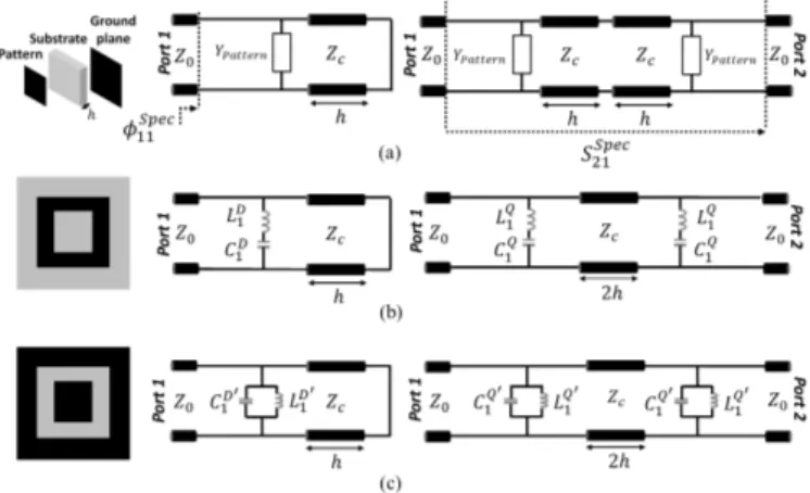
Fig. 2(a)(left) presents the structure of a single layer re-flectarray unit-cell. The structure consists of a metallic layer printed on one side of a single dielectric substrate of thickness hand a metallic ground plane on the other side. Its associated equivalent circuit is represented as a dipolar circuit in Fig. 2(a)(middle). The pattern is represented by a pure imaginary admittance YP attern. The dielectric substrate is modeled by
Fig. 1. General proposed synthesis procedure of a single layer reflectarray unit-cell.
Fig. 2. Single-layer reflectarray unit cell, its dipolar circuit and its associated quadripolar circuit: general case (a), application to metallic-ring cell (b) and slot-ring cell (c).
a transmission line with length h ended by a short circuit which models the metallic ground plane. The objective of the proposed method is to determine YP attern in order to respect
the required reflection phase specification Spec
11 of the dipolar
circuit. Fig. 2(a)(right) presents the symmetrical quadripolar circuit used to make the synthesis compatible with a classical filter synthesis. The reflection phase specification Spec
11 of the
dipolar circuit is then converted into a magnitude transmission specification SSpec
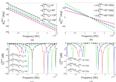
Fig. 3. Variation of the reflection phase specification Spec
11 for different
values of Spec
11 (f0) (a) (for Spec11 = 30 /GHz), Spec 11 (b) (for Spec
11 (f0) = 0 ) and their respectively associated transmission magnitude
specifications |SSpec
21 |dBin (c) and (d).
|SSpec21 (f ))| =
sin
2atan⇣tan( Spec11 (f )
2 ) 2 sin(2 h) ⌘ Spec 11 (f ) 2 ! (1) Fig. 3 presents the reflection phase specifications, Spec
11 , and
their associated transmission magnitude ones |SSpec
21 |dB in two
cases and for a substrate thickness h = 0
4 at f0= 12.5GHz,
the central frequency of our band of interest (10.5-14.5 GHz). First, Spec
11 (f0)varies from 180 to 180 with a constant
phase dispersion Spec
11 = 30 /GHz. Note that the
mag-nitude specification behaves symmetrically according to the sign of Spec
11 (f0). In the following, the results will then be
presented for Spec
11 (f0) 0 only (Fig. 3(a)). Fig. 3(c) shows
that |SSpec
21 |dB has then a third-order band-pass filter behavior
with ripples in the passband and transmission zeros on each side of the passband when Spec
11 = ±180 . The passband
shifts toward high frequencies as Spec
11 (f0) increases (the
shifting is toward low frequencies when Spec
11 (f0)decreases).
This shifting implies a magnitude dissymmetry on the ripple. In fact, if we focus only on the band of interest , the |S21Spec|dB behavior goes from a symmetric band-pass filter
( Spec
11 (f0) = 0 ) to a symmetric band-stop one ( Spec11 (f0) =
180 ) through a set of non-symmetric band-pass or band-stop filters according to the transmission zeros position. Note that we observe the same behavior for Spec
11 (f0) 0 .
Second, Spec
11 (f0)is now fixed (0 in this example) and the
phase dispersion Spec
11 varies from 30 /GHz to 60 /GHz
(Fig. 3(b)). Fig. 3(d) shows that the bandwidth decreases when the phase dispersion increases. The bandwidth decreases as well in the case of a band-stop filter. Note that we observe the same behavior for Spec
11 (f0) 0 .
Fig. 4. Third-order band-stop (a) and band-pass (b) filter prototypes.
Finally, all responses can be approximated either by a third-order band-pass or band-stop Tchebycheff filter according to the band of interest. These prototype filters are used to configure the input and output resonators of the quadripolar circuits with a fixed h. Regarding the unit-cell, a band-stop behavior implies the use of a metallic-ring and a band-pass the use of a slot-ring. In the simplest cases, patches or square apertures can also be used. The two next sections present the synthesis procedure of their respective resonators.
III. SYNTHESIS OF THE SERIES RESONATOR
Fig. 2(b) depicts the top view of a metallic-ring unit-cell, its equivalent dipolar circuit and its associated quadripolar circuit. The metallic-ring is first modeled by a series resonator (LD
1,
CD
1 ) in parallel with a transmission line (length h,
characteris-tic impedance Zc) ended by a short-circuit. The dipolar circuit
is then transformed into a symmetrical quadripolar circuit. Two identical series resonators (LQ
1, C Q
1) are put in parallel
upstream and downstream of a transmission line with length of 2h.
The magnitude behavior of the quadripolar circuit, |S21Spec|dB, is then approximated by a third-order band-stop
filter (Fig. 4(a)) for a given reflection phase specification ( Spec
11 (f0), Spec11 ). The band-stop filter prototype is
syn-thesized to approximate the nearest transmission zero with respect to the band of interest. The first step to configure the filter prototype consists in deducing several parameters from the transmission magnitude specification |SSpec
21 |dB as:
the zero-transmission frequency fSpec
0 ; the cutoff frequency
nearest to the passband fSpec 1 (for
Spec
11 (f0) < 0 ) or f2Spec
(for Spec
11 (f0) > 0 ) and the magnitude ripple LSpecar at the
cutoff frequency. The second step consists in setting the band-stop prototype parameters (central frequency fBS
0 , ripple LBSar , cutoff frequencies fBS 1 and f2BS) as follows: ⇢ fBS 0 = f Spec 0 LBS ar = LSpecar ( fBS 1 = f Spec 1 fBS 2 = fSpec2 0 fBS 1 for Spec 11 (f0) < 0
TABLE I
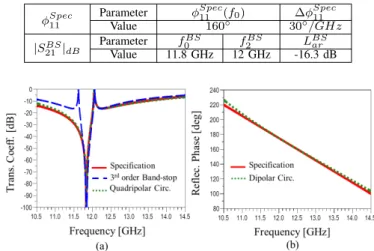
PHASE AND MAGNITUDE PARAMETERS FOR A3rd-ORDER BAND-STOP FILTER APPROXIMATION Spec 11 Parameter Spec 11 (f0) Spec11 Value 160 30 /GHz |SBS 21 |dB Parameter f BS 0 f2BS LBSar Value 11.8 GHz 12 GHz -16.3 dB
Fig. 5. Synthesis of a reflection phase specification Spec
11 presented in Table.
I. Comparison between the transmission magnitudes (a) and reflection phases (b). ( fBS 2 = f Spec 2 fBS 1 = fSpec2 0 fBS 2 for Spec 11 (f0) > 0
The use of classical Tchebycheff band-stop synthesis [7] allows to determine LBS
1 , C1BS, LBS2 and C2BS. We then go
back to the quadripolar circuit with: ⇢
LQ1 = LBS1
C1Q= C1BS.
An example of specifications in phase and magnitude is given in Table. I. Fig. 5(a) presents the response of the corre-sponding third-order band-stop filter, of the realized quadripo-lar circuit and of the initial specification in magnitude. The two latter match very well. Fig. 5(b) shows that the reflection phase of the realized dipolar circuit and the specification also match very well.
However, the band-stop filter approximation reveals some limitations for certain phase range specifications. Fig. 6(a) presents the results of the realized phase for several specifica-tions where Spec
11 (f0)varies from 0 to 180 with a constant
phase dispersion Spec
11 = 30 /GHz. As can be seen, the
phase error between the realized phase and the specification one increases as Spec
11 (f0)decreases from 180 to 0 . This is
actually due to the position of the approximated stop-band with respect to the band of interest. In fact, the transmission zero is shifted toward low frequencies and moved out from the band of interest as Spec
11 (f0) decreases. The phase error depends
also on the phase dispersion Spec
11 . Fig. 7 shows the average
phase errors (solid lines) between the realized phase and the specification one for three phase dispersions Spec
11 in the
band of interest. It can be seen that, for a given Spec
11 (f0), the
average phase error increases as the phase dispersion Spec 11
increases. The average phase error remains under 16 for a
Fig. 6. Comparison between the phase responses of the realized dipolar circuit (dot lines) and the initial specification ones (solid lines) in the case of a third-order (a) band-stop filter approximation and (b) band-pass one .
Fig. 7. Average phase error in the band of interest between the realized phase and the specification one for three dispersion phases Spec
11 =
(30 /GHz, 45 /GHz, 60 /GHz) and in two cases: band-stop approxi-mation and band-pass one.
range of Spec
11 (f0)from 80 to 180 (and symmetrically from
80 to 180 ) for the three phase dispersions.
Eventually, the synthesis of a metallic-ring cell can be achieved by using a third-order band-stop filter synthesis only within this specific phase range. Nevertheless, in order to cover the complementary phase range, the dual cell (using a slot-ring) can be used as we will see now.
IV. SYNTHESIS OF THE PARALLEL RESONATOR
The slot-ring cell is studied in this section. Its topology, dipolar circuit and associated quadripolar circuit are depicted in Fig. 2(c). The slot-ring is modeled by a parallel resonator (LD0
1 ,CD
0
1S) in the dipolar circuit and by two identical parallel
resonators (LQ0
1 ,C Q0
1 ) in its associated quadripolar circuit.
Here, the magnitude behavior of the quadripolar circuit, |S21Spec|dB, is approximated by a third-order band-pass
fil-ter (Fig. 4(b)) for a given reflection phase specification ( Spec
11 (f0), Spec11 ). Unlike the band-stop filter
approxima-tion, the band-pass filter prototype is synthesized to approx-imate the pass-band of |SSpec
21 |dB. The first step here also
consists in deducing several parameters from |SSpec
21 |dB such
as: the magnitude ripple, LSpec
ar , the minimum value in the case
when Spec
11 (f0)6= 0 and the cutoff frequencies (f1Spec,f Spec 2 )
measured at LSpec
ar . The central frequency is then calculated
as follows:
f0Spec= q
f1Specf2Spec.
The second step consists in setting the band-pass prototype parameters (central frequency fBP
0 , cutoff frequencies f1BP
and fBP
2 and ripple LBPar ). These values are then respectively
affected to the prototype parameters (fBP
0 , f1BP, f2BP and
LBP
ar ). The use of classical Tchebycheff band-pass synthesis
[7] allows to determine LBP
1 and C1BP. We then go back to
the quadripolar circuit and affected as well these values to LQ10 and C
Q0
1 . Note that a pre-distortion of the filter response
(small shift in fBP
1 and f2BP) is needed to better match the
expected specifications.
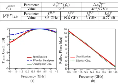
An example of specifications in phase and magnitude is given in Table. II. Fig. 8(a) presents in this case the response of the corresponding third-order band-pass filter, of the re-alized quadripolar circuit and of the initial specification in magnitude. The two latter match very well. Fig. 8(b) shows that the reflection phase of the realized dipolar circuit and the specification also match very well.
However, as in Section. III, the band-pass filter reveals some limitations as well. Fig. 6(b) presents the results of the realized phase for several specifications (see. Section. III). As can be seen, the phase error increases as Spec
11 (f0)increases from 0
to 180 . This is actually due to the location of the pass-band with respect to the band of interest. In fact, it is shifted toward high frequencies and moved out from the band of interest as Spec
11 (f0) increases. Fig. 7(dot lines) shows the average
phase error between the realized phase and the specification one for three phase dispersions Spec
11 in the band of interest.
It can be seen that, for a given Spec
11 (f0), the average phase
error increases as the phase dispersion Spec
11 increases. The
average phase error remains under under 16 but for a range of Spec
11 (f0) from 0 to 80 (and symmetrically from 0 to
80 ) for the three phase dispersions. V. CONCLUSION
In this paper, a method for synthesizing single-layer re-flectarray unit-cell based on filter synthesis techniques was
TABLE II
PHASE AND MAGNITUDE PARAMETERS FOR A3rd-ORDER BAND-PASS FILTER APPROXIMATION Spec 11 Parameter Spec 11 (f0) Spec11 Value 20 45 /GHz |SBP 21 |dB Parameter f BP 1 f2BP f0BP LBPar Value 8.6 GHz 19.8 GHz 13 GHz -0.77 dB
Fig. 8. Synthesis of a reflection phase specification Spec
11 presented in Table.
II. Comparison between the transmission magnitudes (a) and reflection phases (b).
presented. The proposed method allows to convert a reflection phase specification on a dipolar circuit into a transmission magnitude one on a symmetrical quadripolar circuit. The latter can then be easily synthesized with classical filter synthesis techniques. Two complementary cells, a metallic-ring and a slot-ring, were studied in order to achieve a larger phase range specification. These cells were respectively synthesized using a 3rd-order band-stop and band-pass Tchebycheff filter. A
phase range specification of 360 at 12.5 GHz was achieved with an average phase error, in the band of interest 10.5-14.5 GHz, maintained under 16 for a maximum phase dispersion specification of 60 /GHz.
REFERENCES
[1] J. Huang and J. Encinar, Reflectarray Antennas. Wiley Inter-Sciences, 2008.
[2] M. A. Al-Joumayly and N. Behdad, “A generalized method for synthesiz-ing low-profile, band-pass frequency selective surfaces with non-resonant constituting elements,” IEEE Trans. Antennas Propag., vol. 58, no. 12, December 2010.
[3] ——, “Wideband planar microwave lenses using sub-wavelength spatial phase shifters,” IEEE Trans. Antennas Propag., vol. 59, no. 12, December 2011.
[4] A. Edalati and K. Sarabandi, “Reflectarray antenna based on grounded loop-wire miniaturised-element frequency selective surfaces,” IET Mi-crow. Antennas Propag, vol. 8, 2014.
[5] S. M. A. M. H. Abadi, K. Ghaemi, and N. Behdad, “Ultra-wideband, true-time-delay reflectarray antennas using ground-plane-backed, miniaturized-element frequency selective surfaces,” IEEE Trans. Antennas Propag., vol. 63, no. 2, February 2015.
[6] T. Makdissy, R. Gillard, E. Fourn, E. Girard, and H. Legay, “A patch-slot combination approach for large band reflectarrays,” EuRAD, November 2012.
[7] G. Matthaei, E. Jones, and L.Young, Microwave Filters, Impedance-Matching Network, and Coupling Structures. Artech House, Inc., 1980.