HAL Id: hal-01619924
https://hal.archives-ouvertes.fr/hal-01619924
Submitted on 19 Oct 2017
HAL is a multi-disciplinary open access
archive for the deposit and dissemination of
sci-entific research documents, whether they are
pub-lished or not. The documents may come from
teaching and research institutions in France or
abroad, or from public or private research centers.
L’archive ouverte pluridisciplinaire HAL, est
destinée au dépôt et à la diffusion de documents
scientifiques de niveau recherche, publiés ou non,
émanant des établissements d’enseignement et de
recherche français ou étrangers, des laboratoires
publics ou privés.
Power Estimation on FPGAs Based on Signal
Information Propagation Through Digital Operators
Yehya Nasser, Jean-Christophe Prévotet, Maryline Hélard, J Lorandel
To cite this version:
Yehya Nasser, Jean-Christophe Prévotet, Maryline Hélard, J Lorandel. Power Estimation on FPGAs
Based on Signal Information Propagation Through Digital Operators. First International
Confer-ence on Sensors, Networks, Smart and Emerging Technologies (SENSET 2017), Sep 2017, Beyrouth,
Lebanon. �hal-01619924�
Power Estimation on FPGAs Based on Signal
Information Propagation Through Digital Operators
Y. Nasser, J.-C. Pr´evotet, M. H´elard
Institut national des sciences appliqu´ees de Rennes INSA Rennes - IETR
Rennes, France
Email: [email protected]
J. Lorandel
ETIS, UMR 8051, Universit´e Paris Seine Universit´e de Cergy-Pontoise ENSEA, CNRS
Cergy-Pontoise, France
Abstract—Today, communicating devices are widespread and the IoT trend tends to make them incontrovertible in our everyday life. According to some forecast, 50 billions of these devices should be available by 2020. The first consequence is that this massive advent of connecting devices will have a huge impact on the world energy consumption. In this context, it is then mandatory to deal with power as soon as possible in the design process of such systems. This paper presents a new power estimation approach at early design phases which is based on the decomposition of a digital system into a set of basic operators. Each operator has its own model which estimates both switching activity and power consumption. By interconnecting several operators, statistical information is then propagated to enable a global power estimation of a given system. The methodology has been evaluated on a simple use-case. The preliminary results indicate a promising speedup of the design process with less than 8.0% of error compare to classical power estimation tools.
I. INTRODUCTION
Nowadays energy consumption is a major criterion to evalu-ate any electronic system, especially when it comes to systems working at high throughput with restricted energy consumption constraints and these devices will connect billions of services including smart homes, wearable devices, health-care and smart cities, where the major source of power is a battery or an energy harvesting system.
As technology moves forward, new low-power FPGA plat-forms may allow to turn the proposed system into a low power and customizable FPGA-IoT platform[1]. Due to the technological trends towards high-level integration, high op-erating frequencies and low cost, Field Programmable Gate Arrays (FPGAs) constitute one of the best solution for rapid prototyping. These devices have reached such a high level of performance that they constitute an interesting solution to implement IoT functionality. FPGAs are programmable logic devices which can implement any digital function for different fields of application. The major drawback of these devices, compare to their ASICs counterparts, is their relatively high power consumption since they are not optimized for a given application and are far more generic and flexible. It is then even more important to optimize the power consumption in the design flow of such systems and estimate power in various design stages. Power estimation techniques in FPGA can be divided into two categories according to the abstraction level
of the circuit description: low level and high level (system level). At low level, transistors, logic gates and registers are specified and fully described physically, whereas at high level, only a global structure or behavioral view is considered. Generally, this last level lacks from technological details which are crucial to get an accurate information on the dissipated power. Accurate power estimation is achieved at low-level with a significant simulation time that is often prohibitive.
In this paper, a new power estimation technique is presented, which consists of a high-level methodology and proposes the simulation of digital systems based on basic operators. Each operator has been carefully modeled using low-level informa-tion to get accurate results. Combining low-level informainforma-tion and high-level modeling leads to significant speedup of the design process with accurate power estimation.
This paper is organized as follows: Section II presents a small background about the power consumption on FPGAs then related works which describe the existing techniques for power estimation. Section III describes the proposed method-ology. Section IV illustrates the use of our methodology on a case study and provides results. Finally, Section V summarizes the paper.
II. BACKGROUND ANDRELATED WORKS
The total power dissipated has two origins: first the static power, second the dynamic power. Static power is directly related to the transistors’ leakage current. Dynamic power is the power dissipated in a logic design due to switching capaci-tances and short circuit power. Dynamic power is proportional to the switching activity per clock cycle then it is highly data-dependent. The total power consumption expressed in eq. 1
PT otal= PDyn+ PStat= αCVdd2f + VddIleakage (1)
where PDyn is the dynamic power and depends on the
switching activity factor α, the node capacitance C, the supply voltage Vdd, and the frequency f . The static power PStat
is estimated as Vdd Ileakage, where Ileakage represents the
leakage currents. C and Ileakage are technology dependent.
All the presented techniques in the state of the art are methods to estimate the dynamic power consumption which is design dependent.
Today, probabilistic and statistical techniques are the two main types of techniques used for power estimation. Proba-bilistic methodology is based on input probability of a signal pattern to estimate the internal transitions in a digital block. Then, probabilities are propagated from the inputs through the circuit to get the output probability used for the next component [2], [3]. The main drawback in probabilistic meth-ods is that they do not take into account glitches activities and propagation delays. However, these factors have a signif-icant impact on power. Statistical techniques, as presented in [4], are based on a randomly generated input patterns and consist in monitoring power dissipation through a specific power tool. With this approach, accurate results require a huge number of input patterns to cover different scenarios. A significant simulation time is usually deplored and constitutes a critical limitation for these techniques. In the work of [5], a methodology was proposed, based on real measurements, which allows to model power consumption with architectural and algorithmic parameters. Design reuse is a key advantage of this method. In [6], a power estimation technique at RTL level is proposed. It enables the power estimation of a macro (e.g. adder) or an IP directly from the study of the inputs/outputs statistical properties. Their models deliver an average error ranging from 9% to 15%.
III. METHODOLOGY
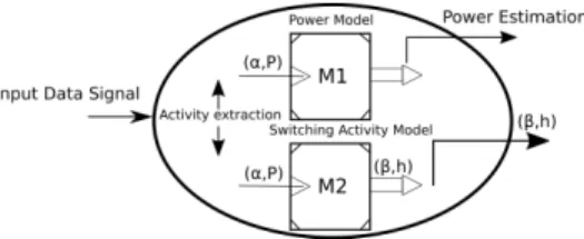
In this work, we will only focus on dynamic power, since it is the type of power that can be optimized during the design. We also made the assumption that any hardware system can be represented by a set of basic operators that exchange data with each other. Each operator may be fully characterized in terms of statistical input/output relationship and power consumption after FPGA implementation. We also provide each component model with two sub-models M 1 and M 2 that are described in Fig. 1. M 1 is used to estimate the dynamic
Fig. 1. Operator Model
power from the signal activity of the operator’s inputs and from the percentage high parameter. It provides an average of the energy consumed during a period of 1s. The signal activity of the inputs is expressed in terms of millions of transitions per second (Mtr/sec) whereas percentage high only represents the time ratio during which the signal is HIGH in a clock period. M 2 enables to estimate the signal activity of the outputs (as well as the percentage high) and is useful when designers want to propagate activity among all operators in order to obtain the power estimation for the full design. The proposed methodology is composed of 2 steps. The first step
is an operator characterization in which each operator is fully implemented in the FPGA. After implementation, a low-level power analyzer is used to estimate the average dynamic power that is consumed by the operator. In this step, We obtain M 1 after timing simulations with randomly generated input metrics i.e. switching activity rate and percentage high. Both (α, p) are the input metrics of the two models while power dissipation and (β, h) are the output metrics for M 1 and M 2 respectively. In the second step, the system is built by connecting different operators. The functionality as well as the power models are described in SystemC in order to ease the interoperability between components. A simple example on the methodology can be described here: for a system composed of N operators, the total power consumption can be derived. Let us assume that the switching activity rate is αi, and that piis the % high at the
input of opi. Therefore (βi,hi) constitutes the output feature
vector of the operator. α1 and p1 respectively correspond to
the switching activity and percentage high at the input of the op1 given by the input stimuli. M1,i and M2,i are the two
models for the opi, then by propagating these information to
the next operators, the total power expressed as in eq. 2.
PGlobal= M1,1(α1, p1) + N −1
X
i=2
M1,i(βi−1, hi−1). (2)
IV. CASE STUDY
As an illustration of the methodology, we have chosen to consider two basic functions i.e a basic multiplier accumulator (MAC) operator, and a parallel to serial converter (P2S) as basic operators.
A. MAC and P2S Operators
The MAC operator is a basic element used in a wide range of applications for digital signal processing. It consists in multiplying two operands and accumulate the result in a dedicated register. Fig. 2 describes an architecture overview of the operator. Note that, this is a simple and generic representation of a MAC unit.
Fig. 2. MAC Architecture
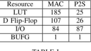
The implementation details in terms of resources are pre-sented in Table I. This table shows the resources of the implemented MAC on FPGA in which the DSP blocks are not used. Note that the target FPGA is a Virtex-7 FPGA: xc7z045ffg900-2.
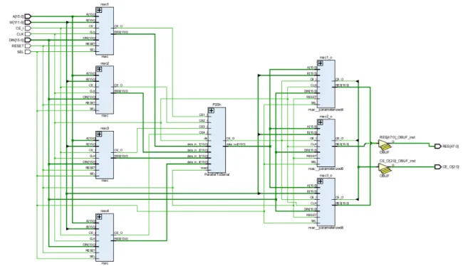
In addition to the MAC operator, a parallel to serial (P2S) operator is described in Fig. 3. This operator aims at receiving 4 inputs (coded into 16 bits) in parallel and to transmit each of these inputs in a serial way to the next block. This module is driven by a clock.
Resource MAC P2S LUT 185 25 D Flip-Flop 107 26 I/O 84 87 BUFG 1 1 TABLE I
REQUIREDRESOURCES FOR BOTHMACANDP2SUNITS ATRT LEVEL
(XC7Z045FFG900-2 FPGA)
Fig. 3. Parallel to Serial Architecture
In order to build both M 1 and M 2 models for the MAC or for the P2S, a first characterization step has been performed. The operator has been implemented on the FPGA target and resources results have been provided. A clock frequency of 200 MHz has been applied to the component.
B. System Build : the Neural Network Example
As an example, A Multi-Layer Perceptron Neural Net-work (MLP) has been studied. The structure of this netNet-work is depicted in Fig. 4. In the forward phase, the hidden layer weight matrix is multiplied by the input vector X = (x1, x2, x3, . . . , xn)
T
to compute the hidden layer output:
yh,j = f Ni X i=1 wh,jixi− θ ! (3)
where wh,ji is the weight connecting input i to unit j in
the hidden neuron layer. θ is an offset termed bias that is also connected to each neuron. In this example, we have chosen not to model the f activation function that would usually require the use of an additional operator based on a simple memory. We assume that this simplification does not hinder the methodology principles and results.
Fig. 4. Structure of a Multi-Layer Perceptron
In our approach, the hardware implementation of neural net-works can be performed using the MAC and the P2S operators. A complete architectural view of a hardware implementation of such network is described in Fig. 5. The example deals with the implementation of a (8 × 4 × 3) MLP. The A inputs consist of 16 bits that are connected to a first MAC layer in order to compute the results of the hidden layer. The w inputs
are used as second inputs of the MAC operators and provide the weights. At the output of the first MAC layer, the results correspond to the outputs of the hidden layer. These results are then sent to the P2S module that serialized them and provide them to the next MAC layer that is used to compute the 3 outputs of the neural network.
A full implementation of the neural network has been performed on a the xc7z045ffg900-2 FPGA target and Table II shows the implementation results in terms of used resources.
Resource Utilization LUT 1313 D Flip-Flops 775 I/O 199 BUFG 1 TABLE II
RESOURCE OFNEURALNETWORK ATRT LEVEL
In order to obtain an estimation of the power consumed by the neural network, we have built a complete model that consists in connecting both M 1 and M 2 models of each involved operator. The complete resulting model is depicted in Fig. 6.
A high level simulation is then performed by giving the same test-bench as in the ”real” implemented neural network. Power estimation is performed in each phase of propagation by storing the values of the power for each operator.
In the next section, detailed results are given that compare the power estimated values from our models with the power values of the global neural network taken from the Xilinx Power Analyzer tool.
C. Results and Discussions
A low-level power estimation tool has been used to esti-mate the power consumption of the complete neural network. The dynamic power consumption of the full design is 239.0 mW. Table III shows the dynamic power consumption of the different operators instances that are used to model the neural network as shown in the Fig. 6. The dynamic power consumption is recorded after each parameters propagation in the proposed model. By summing up the recorded power values, we obtain a total dynamic power estimation of the model as expressed in eq. 4.
Instance Name Operators Dynamic Power (mW)
A Op1 49.0 B Op1 49.0 C Op1 49.0 D Op1 49.0 E Op2 1.0 F Op1 8.0 G Op1 8.0 H Op1 8.0 TABLE III
DYNAMICPOWERESTIMATION OFOPERATORS
Fig. 5. Neural Network architecture at RT Level
Fig. 6. Neural Network Model at High Level
In order to measure the accuracy, the percentage of error (in terms of power estimation) compare to the real implementation at RT level, we have Pref power that results from the real
implementation of the neural network, and Pmethodis the total
power that has been obtained using our models. The obtained results for this implementation show that Pref = 239.0 mW ,
Pmethod = 221.0 mw which corresponds to an estimation
error of only 7.5 %. Note that, the real implementation takes into account all technological details and has a complete knowledge of the placement and routing of the components that are implemented. In fact 8% of error is due to the lack of all the technological information. This result was expected but it seems very promising that dealing with signal activity rates and % of logic high only is enough to obtain a good accuracy and to speedup the design process.
V. CONCLUSION
In this paper, we have proposed a new approach for the FPGA dynamic power estimation, at system level. It is
achieved by the decomposition of a digital system into a set of basic operators. By propagating and summing up the esti-mated power computed for each operator, we obtain a global power estimation. The presented method allows designers to early perform power estimation in the design flow. We have shown that our method provides significant results, since the estimation error is less than 8%. We have then demonstrated that taking the signal activity and percentage HIGH parameters are sufficient enough to obtain a correct accuracy at high level. As future work, we will improve our models based on real power measurements, on various hardware platforms.
REFERENCES
[1] T. Gomes, S. Pinto, T. Gomes, A. Tavares, and J. Cabral, “Towards an fpga-based edge device for the internet of things,” in 2015 IEEE 20th Conference on Emerging Technologies Factory Automation (ETFA), Sept 2015, pp. 1–4.
[2] J. Monteiro, S. Devadas, A. Ghosh, K. Keutzer, and J. White, “Estima-tion of average switching activity in combina“Estima-tional logic circuits using symbolic simulation,” IEEE Transactions on Computer-Aided Design of Integrated Circuits and Systems, vol. 16, no. 1, pp. 121–127, Jan 1997. [3] F. N. Najm, R. Burch, P. Yang, and I. N. Hajj, “Probabilistic simulation
for reliability analysis of cmos vlsi circuits,” IEEE Transactions on Computer-Aided Design of Integrated Circuits and Systems, vol. 9, no. 4, pp. 439–450, Apr 1990.
[4] C. M. Huizer, “Power dissipation analysis of cmos vlsi circuits by means of switch-level simulation,” in Solid-State Circuits Conference, 1990. ESSCIRC ’90. Sixteenth European, vol. 1, Sept 1990, pp. 61–64. [5] D. Elleouet, N. Julien, and D. Houzet, “A high level soc power estimation
based on ip modeling,” in Proceedings 20th IEEE International Parallel Distributed Processing Symposium, April 2006, pp. 4 pp.–.
[6] Y. A. Durrani and T. Riesgo, “Power estimation for intellectual property-based digital systems at the architectural level,” Journal of King Saud University - Computer and Information Sciences, vol. 26, no. 3, pp. 287 – 295, 2014. [Online]. Available: http://www.sciencedirect.com/science/article/pii/S1319157814000068