SILVER NANOWIRE NETWORKS
:
PHYSICAL PROPERTIES AND POTENTIAL INTEGRATION IN SOLAR CELLSHighlights:
Keywords: silver; nanowires; transparent conductive electrodes; photovoltaics; percolation A comparison of different film deposition techniques is made and indicates that the properties of the network are independent of the fabrication method.
Analysis of the electrical behavior as a function of nanowire density is made and compared with theoretical results as well as monte carlo simulations.
Thermal annealing is shown to reduce the sheet resistance from 1000 ohms/sq to 8 ohms/sq. This reduction is achieved by local sintering of the nanowire junctions.
Ag nanowires networks exhibiting a large variation in diffuse transmission are demonstrated, which is important for integration of Ag NW networks into solar cells.
Experimental optimization of Ag nanowire electrodes was undertaken and a peak in the electro-optical properties is observed at approximately 100 mg/m².
Monte carlo simulations are combined with experimental work and percolation theory to explore the electrical behaviour of Ag nanowires networks as a function of density.
A discussion of the potential for integration of Ag Nanowire networks into solar cells is undertaken, summarising some of the examples already in the literature and highlighting key challenges that this emerging material will face as well as the advantages that it offers.
1 2 3 4 5 6 7 8 9 10 11 12 13 14 15 16 17 18 19 20 21 22 23 24 25 26 27 28 29 30 31 32 33 34 35 36 37 38 39 40 41 42 43 44 45 46 47 48 49 50 51 52 53 54 55 56 57 58 59 60 61
SILVER NANOWIRE NETWORKS
:
PHYSICAL PROPERTIES AND POTENTIAL INTEGRATION IN SOLAR CELLSD. P. Langleya,b, G. Giustia, M. Lagrangea, R. Collinsa, C. Jiméneza, Y. Bréchetc , D. Belleta
a)
Laboratoire des Matériaux et du Génie Physique, CNRS-Grenoble INP 3 Parvis Louis Néel, 38016 Grenoble, FRANCE
b)
Laboratoire de Physique des Solides, Interfaces et Nanostructures, Département de Physique, Université de Liège, Allée du 6 Août 17, 4000 Liège, BELGIUM
c)
Laboratoire de Science et Ingénierie des Matériaux et des Procédés CNRS - Grenoble INP, 1130 rue de la piscine
38042 Saint-Martin d’Hères, FRANCE
Corresponding Author: Daniel Langley [email protected] Laboratoire des Matériaux et du Génie Physique, CNRS-Grenoble INP 3 Parvis Louis Néel, 38016 Grenoble, FRANCE
Keywords: silver; nanowires; transparent conductive electrodes; photovoltaics; percolation Abstract
With the growing interest in flexible electronics and the increased utilization of Indium Tin Oxide electrodes for display and photovoltaic applications the need for new materials is emerging.
In this work we present the electro-optical properties of Ag nanowire networks as an alternative transparent conductive material. A comparison of different film deposition techniques is made and indicates that the properties of the network are independent of the fabrication method. Analysis of the electrical behaviour as a function of nanowire density is made and compared with theoretical results as well as Monte Carlo simulations.
Thermal annealing is shown to reduce the sheet resistance from 1000 Ω/sq to 8 Ω/sq, this reduction is achieved by local sintering of the nanowire junctions.
Experimental optimization of Ag nanowire electrodes was undertaken and a peak in the electro-optical properties is observed at approximately 100 mg/m². Finally a discussion of the potential integration of Ag nanowire networks into solar cells is undertaken, we observe that these electrodes show promise as an emerging transparent conductive material, especially for flexible applications.
1- Introduction:
Thin films which exhibit at the same time high electrical conductivity and optical transparency are crucial for many modern electronic devices such e-papers, organic light-emitting diodes (OLEDs), liquid-crystal displays (LCDs), and solar cells. Many articles in the literature currently highlight the growing need to identify and develop new methods and materials for fabrication of transparent conductive materials. There are many reasons for this need and they have been discussed in depth by Kumar et al.[1] and Ellmer.[2]
In the case of solar cells, the transparent electrode usually works as the anode for extracting separated charge carriers from the absorbing area. While transparent conductive oxides (TCOs) are usually well adapted for solar cells, they suffer from significant limitations such as costly fabrication process, scarcity (especially concerning Indium based TCOs like
*Manuscript
1 2 3 4 5 6 7 8 9 10 11 12 13 14 15 16 17 18 19 20 21 22 23 24 25 26 27 28 29 30 31 32 33 34 35 36 37 38 39 40 41 42 43 44 45 46 47 48 49 50 51 52 53 54 55 56 57 58 59 60
Indium Tin Oxide (ITO)) and brittleness. Hence a variety of other materials have been intensively investigated recently.
Kumar et al. highlight three main emerging materials that may provide a useful replacement for transparent conductive oxides (TCOs): Graphene, Carbon Nanotubes and Metallic nanowire networks. Ag NWs already exhibit very good physical properties, but still some issued inhibit the large-scale application of Ag NW electrode as for instance the need of a heating step or the low adhesion of the network onto the substrate. Clearly a better understanding of fundamental properties of Ag NW networks is needed as well thorough investigations of the effects of several parameters such as Ag NW morphology, or the influences of either the experimental conditions and post-deposition treatments (thermal annealing, mechanical pressure, embedding etc.). While the electro-optical properties are of prime importance, other properties are also crucial: electro-mechanical properties (often investigated under bending fatigue), stability (either thermal, chemical), diffuse component of the transmitted light (Haze factor)… This emerging material has only been studied recently and deserves thorough investigations to better its physical properties and facilitate its integration into devices. Alongside all the physical properties, cost will be very important and Ag NW networks can exhibit advantages due to the small required quantity of silver and low-cost deposition techniques.
This article focuses on the physical properties of metallic nanowire networks, specifically silver, and whether this material will provide the necessary balance to meet the needs of photovoltaic applications. In order to obtain a metallic nanowire based transparent electrode which can be efficiently incorporated into a solar cell one can play with several parameters such as the chemical composition and morphology of the metallic nanowires (NW), the density of the NW network and the use of post processing such as mechanical pressing[3,4], chemical treatments[5] and thermal annealing[3,6]. We report here the influence of the density and annealing on the physical properties of Ag NW networks pertinent to their potential integration into a solar cell.
2- Experimental section:
Ag NWs dispersed in isopropyl alcohol were acquired from Seashell Technology.[7] The average dimensions of the nanowires were 0.105 µm for the diameter and 37.5 µm for the length resulting in an aspect ratio of about 360. Films of different density were fabricated from suspensions of different concentrations. Random AgNW networks were generated by different techniques including spin-coating, drop casting, rod coating and spray injection (as described in Ref. [8]) on low alkaline earth boro-aluminosilicate glass (Corning C1737-S111).
Field-emission scanning electron microscopy (FESEM) imaging was recorded with a FEI Quanta 250 to investigate the network morphology.
In-situ thermal annealing under atmosphere combined with real time electrical resistance acquisition using the two-point probe method and with a constant voltage of 1V was performed to gain insight into the thermal behavior of the Ag NW networks. Silver paint strips acted as electrical contacts and the total sample size was 12.5 by 12.5 mm. Thus, the resistance values reported in this study represent an average over the surface previously mentioned.
The optical transmittance was recorded by using a Lambda 950 Perkin Elmer spectrophotometer. No substrate subtractions were performed on any of the film reported in this study. In addition, optical transmission values are quoted at λ=550 nm. The haze factor, quantifying the amount of light scattering, was calculated from the total (T(total)) and direct (T(direct)) transmittances by (T(total)-T(direct))/T(total).
1 2 3 4 5 6 7 8 9 10 11 12 13 14 15 16 17 18 19 20 21 22 23 24 25 26 27 28 29 30 31 32 33 34 35 36 37 38 39 40 41 42 43 44 45 46 47 48 49 50 51 52 53 54 55 56 57 58 59 60 61
Four point probe measurements were performed using a Keithley 2400 sourcemeter with a Lucas Labs Pro4-440N probe station.
3- Results and discussions
Electro-optical properties:
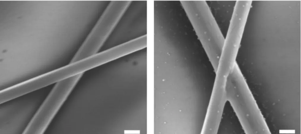
Of the properties that are desirable for Transparent Conductive Materials (TCMs) the obvious selection criteria are the transmission of light and the electrical resistance. Considering this, it is appropriate to make an initial comparison of AgNW networks electro-optical properties with those of TCOs. All electro-electro-optical properties that are discussed are measured on AgNW networks after a thermal annealing step which was found to significantly decrease the resistance without having an impact on their transmittance. The changes of resistance are due to several factors that will not be discussed in depth here but in majority are caused by local sintering at the junctions between the nanowires (as shown by Figure 1). The local sintering occurs as a result of atomic migration to reduce the surface energy at points of high curvature. Figure 1 exhibits Scanning Electron Microscopy observation of two different junctions between two nanowires before and after annealing for two hours at 200°C in air. Although this is not the same junction before and after annealing these images represent typical morphologies. Local sintering at the junction is present after annealing, which leads to a decrease of sheet electrical resistance from 1000 to 8 sq.
Figure 1: SEM images of AgNW junctions before (left) and after (right) annealing, the sheet resistance of this network reduced from 1000sq to 8sq. Scale bars indicate 100 nm.
The reduction of resistance via thermal annealing allows the production of highly conductive layers. Modifying the annealing profile enables networks with Rs<20 /sq to be
created with 2 minutes at 250°C or if there is a temperature restriction the same can be achieved with a longer annealing at lower temperatures. At 200°C the network resistance continues to drop for 2 hours though the majority of the change occurs in the first 5 minutes.
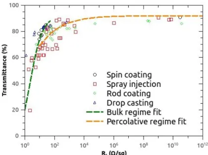
The resistance and transmittance of AgNW networks are dependent on the wire length and diameter as well as the density of the network.[9] The nanowire diameter plays a key role in the scattering properties of the network as highlighted by Preston et al. [10]. It is common to plot the Transmittance as a function of sheet resistance[11]. Figure 2 shows that the general behavior of transmittance is somewhat independent of deposition method.
1 2 3 4 5 6 7 8 9 10 11 12 13 14 15 16 17 18 19 20 21 22 23 24 25 26 27 28 29 30 31 32 33 34 35 36 37 38 39 40 41 42 43 44 45 46 47 48 49 50 51 52 53 54 55 56 57 58 59 60
Figure 2: a) Optical transmittance at 550 nm (including the substrate contribution) versus the sheet resistance after annealing, for different deposition techniques: spin coating, rod coating, drop casting and spray injection The green line represent fits to the bulk regime while the red line represent fits to the percolative regime (see Ref. [4] for more details on the equations used).
A comparison of AgNW networks, silver flakes, carbon nanotubes and graphene was also made by De et al.[11] Their results concern NW networks created by vacuum filtration of a colloidal solution of AgNW onto a membrane to form the network, which is then transferred to a PET substrate. The experimental results of the current contribution are presented in Figure 2 for AgNW networks generated by the various techniques mentioned in the legend of the figure. The comparison of these results with those of De et al. [11] suggests that there is only a slight dependence of electro-optical properties of AgNW networks on the deposition method used. The majority of the behavior is dominated by the geometry of the wires. In strong agreement with the work of De et al.[11], the data fits well in both regimes: the percolation regime for sparse networks and bulk regime for dense networks. As discussed below an optimal density has to be considered to reach a tradeoff in order to get high optical transmittance T and low sheet resistance RS. Generally speaking a good quality transparent
electrode for solar applications corresponds roughly to: T ≈ 90% and RS ≈10 sq. When
considering the substrate contribution, as in Figure 2, such requirements would lead to T ≈ 80%. As depicted by Figure 2, Ag NWs already meet the requirements for being an efficient transparent electrode for solar cells applications.
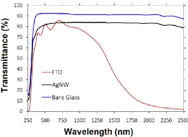
Figure 3 shows a comparison of the transmission spectra for bare glass, AgNW network and Fluorine doped Tin Oxide (FTO), and illustrates the important difference in the transmission spectrum of AgNW when compared to standard TCOs. There are very similar transmission values from 250-1250 nm at which point a significantly higher rate of transmission is observed for the AgNW network in the region 1250–2500 nm. This stems from the plasmon absorption of TCOs: above a certain wavelength P (which depends upon
the carrier density) the electromagnetic wave is damped thanks to the collective excitation of the carrier gas.[2] Increasing the carrier density (by doping) in most TCOs results in a decrease of P leading to a trade off in transparency to gain conductivity. This again
1 2 3 4 5 6 7 8 9 10 11 12 13 14 15 16 17 18 19 20 21 22 23 24 25 26 27 28 29 30 31 32 33 34 35 36 37 38 39 40 41 42 43 44 45 46 47 48 49 50 51 52 53 54 55 56 57 58 59 60 61
illustrates the need to determine an optimal carrier concentration which balances conductivity and transmission. This provides an immediate advantage for Ag NW networks integration for solar cells employing low band gap active regions or tandem cell architecture. As the infra red component of the solar spectrum can be transmitted into the cell it can be used for energy production. The origin of the absorbance of the TCO is a result of the material being a continuous thin film. Unlike TCOs which absorb light for >P the NW networks provide a
large amount of empty space between wires that allow light to pass between the wires without being absorbed.
Figure 3. Total transmission spectra of a glass substrate (blue), an Ag NWs network (black) and fluorine doped tin oxide (FTO) (red). The associated sheet electrical resistance for Ag NW network and FTO are 9.5 Ω/sq, and 7.4 Ω/sq, respectively.
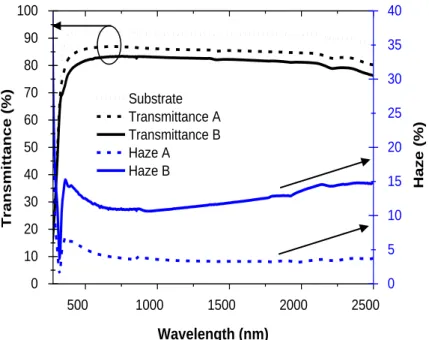
The slightly higher average transmittance of the AgNW film in the 250-1250 nm range indicates that silver nanowires provide a promising alternative to some TCOs in terms of electro-optical properties. Furthermore, recent studies have shown that increasing the haze factor (ratio of diffuse light to total transmitted light) of a given transparent electrode can help to improve the efficiency of a solar cell.[12] Light scattering increases the path length of light through the absorber layer of a solar cell and consequently increases the current generated in the solar cell.[13] The haze factor of an Ag NW network is dependent upon several key factors: length and diameter of the wires used, NW density and fabrication method. It is possible to achieve a significant increase in the haze factor with only a small tradeoff in optical transmission. As shown in Figure 4 it is possible to achieve a 3 fold increase in the average haze factor and only takes 2-3% from the optical transmission. This tradeoff is also balanced to a certain extent in that the electrical resistance of electrode B is 9.5 Ω/sq as compared to 17.3 Ω/sq for electrode A.
1 2 3 4 5 6 7 8 9 10 11 12 13 14 15 16 17 18 19 20 21 22 23 24 25 26 27 28 29 30 31 32 33 34 35 36 37 38 39 40 41 42 43 44 45 46 47 48 49 50 51 52 53 54 55 56 57 58 59 60
Figure 4: Transmittance spectra (upper curves, dotted line is the bare glass substrate, dashed and solid lines are AgNW networks of different density: A) 57mg/m2 and B) 117mg/m2) and the related haze spectra of the same samples (lower curves).
As stated, the haze factor of a AgNW network is determined by NW density amongst other properties of the network. Intuitively, it would seem that decreasing the NW density per unit area, n, should lead to higher optical transparency. It is by no means a direct relationship, as complex scattering and graduated refractive indices convolute the relationship of density to transmission.[10] In a simple model though, it is possible to calculate the approximate transmission and this follows to some extent the intuitive idea, decreasing density results in higher optical transparency. However, the electrical resistance of the NW networks is also density dependent. Again the trade off emerges with a three way balance that needs to be struck to produce the optimal network. The relationship of the network resistance to NW density can be defined as a percolation problem. Several works in the past have devoted effort to understanding the problem of 2D conductive stick percolation. For instance Pike and Seager[14] and Li and Zhang[15] produced some excellent theoretical results that defined the problem in its infancy and have led to further understanding of the problem. Application of percolation theory so far has mainly been restricted to theoretical works and it is a good opportunity to observe whether the theory supports the experimental data for Ag NW networks. Coleman’s group has already applied percolation theory to Transmission data.[16] We focus below more on the electrical properties.
Reducing the number of NWs per unit area creates a sparser network that may fail to form enough conducting paths across the network. For low density, i.e. in the percolation regime, the properties of the network differ from the bulk material values. In this percolating regime the electrical conductivity dc depends on the NW density n and follows a power
scaling law:
tC dc nn
eq.(1)
where nc is the percolation threshold and t is the universal conductivity exponent
(equal to 1.29) [17], [18]. Eq.(1) is valid when n is larger, but close, to nc. The percolation
threshold of a system can be defined by the density of the sticks at which there is a 50% chance that a network with that density will have a percolating cluster that spans through the
500 1000 1500 2000 2500 0 10 20 30 40 50 60 70 80 90 100 Substrate Transmittance A Transmittance B Haze A Haze B Wavelength (nm) Trans mit tance (%) 0 5 10 15 20 25 30 35 40 Ha ze (% )
1 2 3 4 5 6 7 8 9 10 11 12 13 14 15 16 17 18 19 20 21 22 23 24 25 26 27 28 29 30 31 32 33 34 35 36 37 38 39 40 41 42 43 44 45 46 47 48 49 50 51 52 53 54 55 56 57 58 59 60 61
considered system. For large systems with nanowires of length l, it has been found that the critical number density nc as defined by Li and Zhang[15]:
2 00002 . 0 63726 . 5 l nc eq.(2)
Equation 2 clearly states that longer nanowires are associated with a lower percolation NW density. However eq(2) is only valid in the consideration of large scale systems, while for the purpose of photovoltaics and many other applications this requirement is not always met.
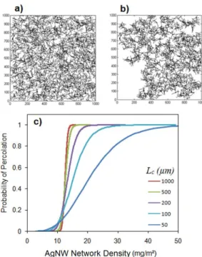
Figure 5: a) Simulated image of the 1000x1000 m2 network, b) same network with wires that are not part of the percolating cluster removed, c) Graph showing the probability of percolation versus the Ag NW network density for various characteristic lengths of percolation (LC). Decreasing the length of percolation results in an increase in the density
required to reach the percolation threshold.
The density of nanowires required to make a percolating network has a minimum value as defined by eq(2). However this value is only accurate for large systems where the ratio of the system size to nanowires length is greater than 30.[15] In the network shown in figure 5 a) and b) it is clear that there are some regions of the network will not contribute to the conduction pathway or in a solar cell to the collection of photo generated electrons. This will result in reduced collection efficiency for nanowire based electrodes.
In order to determine the density required to produce a network which has a higher percentage of the network contributing to the percolating cluster a characteristic length can be defined. Defining this length Lc as the minimum distance over which the probability of
percolation at the given density nc is equal to 50% we can then simulate the required densities
for various values of Lc. Fig. 5 c) is a result of Monte Carlo simulations performed using the
fast Monte Carlo method of Newman and Ziff [19] and displays the effect of decreasing Lc
which corresponds to an increase in nc. This result is rather intuitive since a high collection
efficiency should be associated to percolation clusters occurring on a shorter scale which is associated with a higher Ag NW network density.
1 2 3 4 5 6 7 8 9 10 11 12 13 14 15 16 17 18 19 20 21 22 23 24 25 26 27 28 29 30 31 32 33 34 35 36 37 38 39 40 41 42 43 44 45 46 47 48 49 50 51 52 53 54 55 56 57 58 59 60
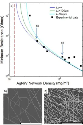
For exploring the influence of the network density one should investigate the dependence of both the electrical resistance and optical transparency (usually considered at a wavelength of 550 nm). The electrical resistance of Ag NW networks versus density is reported in Figure 6.
The vertical dotted line indicates the value of nc as defined in eq.(2). The electrical
resistance corresponds to the minimum electrical resistance measured in-situ during a thermal annealing with a ramp of 15K/min. As discussed above, thermal annealing causes a decrease of the resistance, by reducing the junction resistance between adjacent nanowires. However longer annealing or annealing at higher temperature can cause the morphological change of Ag NWs (leading eventually to sphereodization) which then prevents the network from percolating. Therefore a minimum of sheet resistance is observed during a thermal annealing ramp.
The blue line in Figure 6 corresponds to a fit using both eq.(1) and (2) which consider percolation over an infinite size system. A good agreement is observed, showing that the percolation regime is valid for the whole network density range investigated. As already mentioned, any experimental values are certainly not necessarily associated with infinite size system but with finite system size over which the percolation is observed. Experimentally we observe the percolation and electrical behavior in effectively infinite systems, it is expected therefore that the electronic behavior will match that of the theoretical infinite system. In fact as shown in Figure 6 a finite value of Lc=50µm constitutes a better agreement with
experimental data. This does not suggest that the critical density is in some way restricted in these experiments, but indicates that the network density is in fact sufficiently dense as to provide percolation to a large proportion of the network.
Figure 6: a) Experimental resistance values as a function of network density. The blue line on the graph represents a curve fitted to the data using eq.(1) and eq.(2), associated to an infinite system. The other curves are associated with two different Lc values (Lc=100 µm and
1 2 3 4 5 6 7 8 9 10 11 12 13 14 15 16 17 18 19 20 21 22 23 24 25 26 27 28 29 30 31 32 33 34 35 36 37 38 39 40 41 42 43 44 45 46 47 48 49 50 51 52 53 54 55 56 57 58 59 60 61
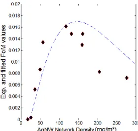
The optical transmittance can also be investigated versus the NW density and the Lambert-Beer law is usually employed as a first approximation [11]. The data of the present study is in good agreement with this approach and is used to simulate the properties of the Ag NW networks when calculating the figure of merit of the obtained transparent electrode.
A commonly used figure-of-merit for transparent conducting electrodes is defined by Haacke [20]: sh H R T10 eq. (3)
Where T is the optical transmittance and Rsh is the electrical sheet resistance. The
experimental values of are reported in Figure 7. An optimal density is observed close to a NW mass density of 120 mg/m2 which is associated to a sheet resistance of 9.5 sq and a total transmittance of 82.9% without removing the losses due to the substrate. Subtraction of the substrate leads to a total transmittance of about 90%. The dotted line of figure 7 corresponds to the calculated figure-of-merit values using eq.(1), eq.(2) and eq.(3) as well as the Lambert-Beer law. A reasonable agreement is obtained between the calculated and experimental values, especially considering the simplicity of the model used. This clearly indicates that the optimal Ag NW density which considers to the tradeoff between high optical transparency and low electrical resistance is close to about 100 mg/m2. This would correspond to the same amount of silver (for a given area) as a thin silver film of 10 nm thick as compared to 200-300 nm for usual TCOs. The observed optimal Ag NW network density observed in Fig.7 is in rather good agreement with the results obtained by De et al. [De ACS 2009] who found optimal performances for a density of 47 mg/m2 but with different Ag NW morphological parameter and with another deposition technique. Finally the obtained value (16x10-3) is comparable to some TCOs except for the best ITO thin films.[2]
Figure 7: Experimental (symbols) and calculated (dotted line) values of the figure of merit defined by eq.(3) versus the Ag NW network density.
Potential for incorporation into solar cells
Many groups have already started to incorporate silver nanowires as front electrodes for solar applications.[21-24] As mentioned, high haze factors result in light scattering into the device and increases the effective absorption cross section. The ability of AgNW networks to produce high haze networks while maintaining sufficient electro-optical properties shows the real potential to integrate them into solar cells. Gaynor et al.[23]
1 2 3 4 5 6 7 8 9 10 11 12 13 14 15 16 17 18 19 20 21 22 23 24 25 26 27 28 29 30 31 32 33 34 35 36 37 38 39 40 41 42 43 44 45 46 47 48 49 50 51 52 53 54 55 56 57 58 59 60
demonstrated an increase of approximately 10% in conversion efficiency of bulk organic hetero-junction solar cells, by using a AgNW composite electrode as compared to an ITO standard (ɳ =3.4% using ITO on plastic and ɳ =3.8% for Ag nanowire composite). Taking advantage of the metal nanowire network transparency in the infra-red region of the spectrum Chen et al. [22] created polymer solar cells that were semi-transparent in the visible region and had an ɳ ≈4%. These cells have an average transmission of about 61% in the 450-650 nm wavelength range.[22] This type of solar cell could for instance be used as an energy producing window tinting. Another advantage of AgNW networks as front electrodes for photovoltaic applications is that they allow production of flexible solar cells,[21] which is difficult to achieve with TCOs due to their brittleness. Within the field of photovoltaics there are many different device architectures which have restrictions associated with them, for some such as Dye Sensitized Solar Cells and CdTe, the transparent electrode must be deposited first with high temperature processes to follow. CIGS solar cells on the other hand generally require that the TCM is added last and has to be deposited at low temperature to prevent diffusion of the active layers into one another. Depending in which application the AgNW electrodes are to be employed the processing steps required will differ. Kim et al. [25] demonstrated the incorporation of ZnO/AgNW/ZnO multilayer electrode into CIGSSe solar cells and also demonstrated that ZnO encapsulation improves the thermal stability of AgNWs. Improved thermal stability by encapsulation has also be shown by several other groups,[8, 26, 27] and there are several low temperature routes to highly conductive AgNW networks,[3-5] hence there are many options to support the application of AgNWs to a broad variety of solar cell architectures.
In considering the incorporation of AgNW networks into solar cells we must also consider the fact that the network presents a discontinuous film. This means that as a function of position relative to the network the probability of a photo-generated electron being collected will vary. This is especially important when considering the mobility of electrons in the active region of the cell. For cells where electrons and excitons can support a long diffusion length to the collecting electrode, AgNW networks provide an interesting and viable solution as a front electrode. When the diffusion length is below 1µm such as in organic solar cells, AgNW networks alone are insufficient. However as shown by Kim et al. the incorporation of AgNW network embedded in a conductive matrix can aid in the collection efficiency.[25] In this case the AgNW network is used to provide the majority of the electrical performance of the electrode and the matrix material allows continuous conductivity. In this manner, materials which have a low mobility such as PEDOT:PSS may be enhanced.
Let us also note that roughness can be an issue: if some nanowires are not well aligned along the substrate some short-circuits could then occur. The use of high mechanical pressure has been shown to overcome such problems.[4] As a final remark it is worth mentioning that embedding Ag NWs within a transparent oxide such as ZnO or TiO2 could
be interesting, for instance the Ag NWs stability (either chemical or thermal) could be improved and properties such as work function could be tuned. This might help as well with the integration of Ag NWs into a solar cell, since band alignment plays a crucial role for the solar cell efficiency.
Conclusions
Random Ag networks demonstrate electro-optical properties close to that of TCO materials. They depend both on the morphology of the metallic nanowires (NW) and the density of the NW network. Post processing treatments also play an important role in the
1 2 3 4 5 6 7 8 9 10 11 12 13 14 15 16 17 18 19 20 21 22 23 24 25 26 27 28 29 30 31 32 33 34 35 36 37 38 39 40 41 42 43 44 45 46 47 48 49 50 51 52 53 54 55 56 57 58 59 60 61
resulting electro-optical properties. Several of these treatments are investigated in the literature suggesting that the gap with TCOs could be bridged in the near future. Furthermore, as reported in the present study of such random networks, simulation is a valuable tool to gain more insight into the electro-optical properties. From Monte-Carlo simulations, it was found that decreasing the characteristic length of percolation resulted in increasing the density of nanowires required to reach the percolation threshold. From this work, it is clear that AgNW networks currently provide sufficient electro-optical properties to be incorporated into solar cells. Although not yet matching the best ITO films in terms of optimal sheet resistance and transmittance, AgNWs provide sufficient properties and are expected to continue to improve. They are amenable to low deposition temperatures, solution processing, flexibility and variable haze of the resulting electrode. These aspects suggest that this material could become more important in emerging applications, particularly in the field of photovoltaics in which indium-free transparent electrodes should emerge in a near future.
Acknowledgements:
We thank E. Bellet-Amalric and M. Anikin for their help in thin films characterization, D. Nguyen for fruitful discussions. This work has been supported by Grenoble INP through the SEI grant and Erasmus Mundus through the IDS FunMat Program.
References:
[1] A. Kumar and C. Zhou, “The Race To Replace Tin-Doped Indium Oxide: Which Material Will Win?,” ACS Nano, vol. 4, no. 1, pp. 11–14, 2010.
[2] K. Ellmer, “Past achievements and future challenges in the development of optically transparent electrodes,” Nat. Photonics, vol. 6, no. 12, pp. 809–817, 2012.
[3] L. Hu, H. S. Kim, J.-Y. Lee, P. Peumans, and Y. Cui, “Scalable Coating and Properties of Transparent, Flexible, Silver Nanowire Electrodes,” ACS Nano, vol. 4, no. 5, pp. 2955– 2963, 2010.
[4] T. Tokuno, M. Nogi, J. Jiu, T. Sugahara, and K. Suganuma, “Transparent Electrodes Fabricated via the Self-Assembly of Silver Nanowires Using a Bubble Template,”
Langmuir, vol. 28, no. 25, pp. 9298–9302, 2012.
[5] C. H. Liu and X. Yu, “Silver nanowire-based transparent, flexible, and conductive thin film,” Nanoscale Res. Lett., vol. 6, no. 75, pp. 1–8, 2011.
[6] J.-Y. Lee, S. T. Connor, Y. Cui, and P. Peumans, “Solution-Processed Metal Nanowire Mesh Transparent Electrodes,” Nano Lett., vol. 8, no. 2, pp. 689–692, Feb. 2008. [7] “http://www.seashelltech.com/index.shtml,” Accessed 06 July 2013.
[8] G. Giusti, D. Langley, C. Jiménez, E. Puyoo, A. Muthukumar, E. Appert, V. Consonni, and D. Bellet, “Fabrication of Transparent Conductive Thin Film Electrodes Based on Ag Nanowire on Transparent Substrates Using the Spray Method for Photovoltaic
Applications,” MRS Online Proc. Libr., vol. 1439, pp. 51–56, 2012.
[9] S. Sorel, P. E. Lyons, S. De, J. C. Dickerson, and J. N. Coleman, “The dependence of the optoelectrical properties of silver nanowire networks on nanowire length and diameter,”
Nanotechnology, vol. 23, no. 18, p. 185201, May 2012.
[10] C. Preston, Y. Xu, X. Han, J. N. Munday, and L. Hu, “Optical haze of transparent and conductive silver nanowire films,” Nano Res., p. In Press, May 2013.
[11] S. De, P. J. King, P. E. Lyons, U. Khan, and J. N. Coleman, “Size Effects and the Problem with Percolation in Nanostructured Transparent Conductors,” ACS Nano, vol. 4, no. 12, pp. 7064–7072, 2010.
1 2 3 4 5 6 7 8 9 10 11 12 13 14 15 16 17 18 19 20 21 22 23 24 25 26 27 28 29 30 31 32 33 34 35 36 37 38 39 40 41 42 43 44 45 46 47 48 49 50 51 52 53 54 55 56 57 58 59 60
[12] T. Chih-Hung, H. Sui-Ying, H. Tsung-Wei, T. Yu-Tang, C. Yan-Fang, Y. H. Jhang, L. Hsieh, W. Chung-Chih, C. Yen-Shan, C. Chieh-Wei, and L. Chung-Chun, “Influences of textures in fluorine-doped tin oxide on characteristics of dye-sensitized solar cells,”
Org. Electron., vol. 12, no. 12, pp. 2003–2011, Dec. 2011.
[13] D. S. Hecht, L. Hu, and G. Irvin, “Emerging transparent electrodes based on thin films of carbon nanotubes, graphene, and metallic nanostructures,” Adv. Mater., vol. 23, no. 13, pp. 1482–1513, 2011.
[14] G. E. Pike and C. H. Seager, “Percolation and conductivity: A computer study. I,”
Phys. Rev. B, vol. 10, no. 4, pp. 1421–1434, 1974.
[15] J. Li and S.-L. Zhang, “Finite-size scaling in stick percolation,” Phys. Rev. E, vol. 80, no. 4, pp. 040104–040104–4, Oct. 2009.
[16] S. De, T. M. Higgins, P. E. Lyons, E. M. Doherty, P. N. Nirmalraj, W. J. Blau, J. J. Boland, and J. N. Coleman, “Silver Nanowire Networks as Flexible, Transparent,
Conducting Films: Extremely High DC to Optical Conductivity Ratios,” ACS Nano, vol. 3, no. 7, pp. 1767–1774, 2009.
[17] M. Žeželj and I. Stanković, “From percolating to dense random stick networks: Conductivity model investigation,” Phys. Rev. B, vol. 86, no. 13, pp. 134202–134202–6, Oct. 2012.
[18] D. Stauffer and A. Aharony, Introduction to Percolation Theory, 2nd revised ed. London: Taylor and Francis, 2003.
[19] M. E. J. Newman and R. M. Ziff, “Fast Monte Carlo algorithm for site or bond percolation,” Phys. Rev. E, vol. 64, no. 1, pp. 016706–016706–16, Jun. 2001.
[20] G. Haacke, “New figure of merit for transparent conductors,” J. Appl. Phys., vol. 47, no. 9, pp. 4086–4089, 1976.
[21] L. Yang, T. Zhang, H. Zhou, S. C. Price, B. J. Wiley, and W. You, “Solution-Processed Flexible Polymer Solar Cells with Silver Nanowire Electrodes,” ACS Appl
Mater Interfaces, vol. 3, no. 10, pp. 4075–4084, 2011.
[22] C.-C. Chen, L. Dou, R. Zhu, C.-H. Chung, T.-B. Song, Y. B. Zheng, S. Hawks, G. Li, P. S. Weiss, and Y. Yang, “Visibly Transparent Polymer Solar Cells Produced by
Solution Processing,” ACS Nano, vol. 6, no. 8, pp. 7185–7190, Aug. 2012.
[23] W. Gaynor, J.-Y. Lee, and P. Peumans, “Fully Solution-Processed Inverted Polymer Solar Cells with Laminated Nanowire Electrodes,” ACS Nano, vol. 4, no. 1, pp. 30–34, Jan. 2010.
[24] F. S. F. Morgenstern, D. Kabra, S. Massip, T. J. K. Brenner, P. E. Lyons, J. N. Coleman, and R. H. Friend, “Ag-nanowire films coated with ZnO nanoparticles as a transparent electrode for solar cells,” Appl. Phys. Lett., vol. 99, no. 18, pp. 183307– 183307–3, 2011.
[25] A. Kim, Y. Won, K. Woo, C.-H. Kim, and J. Moon, “Highly Transparent Low
Resistance ZnO/Ag Nanowire/ZnO Composite Electrode for Thin Film Solar Cells,” ACS
Nano, vol. 7, no. 2, pp. 1081–1091, Feb. 2013.
[26] A. Mayoral, L. F. Allard, D. Ferrer, R. Esparza, and M. Jose-Yacaman, “On the behavior of Ag nanowires under high temperature: in situ characterization by aberration-corrected STEM,” J Mater Chem, vol. 21, no. 3, pp. 893–898, 2010.
[27] P. Ramasamy, D.-M. Seo, S.-H. Kim, and J. Kim, “Effects of TiO2 shells on optical and thermal properties of silver nanowires,” J. Mater. Chem., vol. 22, no. 23, pp. 11651– 11657, May 2012.
Figure1
Figure2
Figure 3
0 10 20 30 40 50 60 70 80 90 100 Substrate T ransmittance A T ransmittance B Haze A Haze B T r a n s m i t t a n c e ( % ) 0 5 10 15 20 25 30 35 40 H a ze ( % ) Figure4
Figure5
Figure6
Figure7