HAL Id: hal-00872304
https://hal.archives-ouvertes.fr/hal-00872304
Submitted on 11 Oct 2013
HAL is a multi-disciplinary open access
archive for the deposit and dissemination of
sci-entific research documents, whether they are
pub-lished or not. The documents may come from
teaching and research institutions in France or
abroad, or from public or private research centers.
L’archive ouverte pluridisciplinaire HAL, est
destinée au dépôt et à la diffusion de documents
scientifiques de niveau recherche, publiés ou non,
émanant des établissements d’enseignement et de
recherche français ou étrangers, des laboratoires
publics ou privés.
Auto-Scale Factor algorithm for MIMO channel
hardware simulator: Toward higher and stable SNR
Bachir Habib, Gheorghe Zaharia, Ghaïs El Zein
To cite this version:
Bachir Habib, Gheorghe Zaharia, Ghaïs El Zein. Auto-Scale Factor algorithm for MIMO channel
hardware simulator: Toward higher and stable SNR. International Journal of Research in Wireless
Systems (IJRWS), 2013, 2 (29), pp.31-43. �10.2320-3617�. �hal-00872304�
International Journal of Research in Wireless Systems (IJRWS), Volume 2, Issue 29, (2013) 1
hardware simulator: Toward higher and stable SNR
Bachir Habib, Gheorghe Zaharia, Ghais El Zein
Institute of Electronics and Telecommunications of Rennes, IETR, UMR CNRS 6164, France [email protected]
ABSTRACT
A hardware simulator facilitates the test and validation cycles by replicating channel artefacts in a controllable and repeatable laboratory environment. In this paper, a new Auto-Scale Factor (ASF) based architecture of the digital block of the hardware simulator for MIMO radio propagation channel is introduced. A detailed study shows that this architecture increases the Signal-to-Noise Ratio (SNR) of the output signals when the input signals or the impulse responses of the channel (h) are attenuated. The architecture is implemented on a Xilinx Virtex-IV FPGA. the occupation on the FPGA and the accuracy of this architecture are analyzed.
KEYWORDS:
CONCLUSION
To decrease the error at the output of the hardware simulator, an ASF-based architecture is used. A detailed study shows that for high attenuation of the impulse responses and the input signal, the SNR of the output signals increases significantly. The average global SNR is increased by 37 dB for -/+ 7 dB variation of h in time. Moreover, it can attend 100 dB for an attenuation up to 15 dB of the impulse responses. Simulations will be made using a Virtex-VII [1] platform will allow us to simulate up to 8×8 MIMO channels and higher. A graphical user interface will be designed to allow the user to reconfigure the channel parameters. Also, cognitive hardware simulator for heterogeneous environments will be realized.
AUTO-SCALE FACTOR ALGORYTHM FOR MIMO CHANNEL HARDWARE SIMULATOR: TOWARD HIGHER AND STABLE SNR
International Journal of Research in Wireless Systems (IJRWS), Volume 2, Issue 29 (2013) 2 N=14 bits 01010011001100
16 bits
I. INTRODUCTION
The architecture of the digital block of the hardware simulator is mapped onto a Field Programmable Gate Array (FPGA) Virtex-IV [1] that has a great flexibility in algorithm design [2]. The channel models can be obtained from standard models, as the TGn 802.11n [3] and the 3GPP-LTE models [4], or from measurements conducted with the MIMO channel sounder designed and realized at IETR [5]. In the MIMO context, little experimental results have been obtained regarding time-variations, partly due to several limitations of the channel sounding equipment [6]. However, theoretical models of time-varying channels can be obtained using Rayleigh fading and Kronecker correlation-based model [7].
At IETR, several architectures of the digital block of a hardware simulator have been studied [8]. Typically, radio propagation channels are simulated using Finite Impulse Response (FIR) filters, as in [8, 9]. The Fast Fourier Transform (FFT) modules with algebraic product can also be used, as in [8, 10]. However, these considered frequency architectures operate correctly for signals not exceeding the FFT size. Thus, new frequency architecture avoiding this limitation has been presented and tested [11, 12]. Moreover, [12, 13] show that the time domain architecture is better in terms of occupation on FPGA, output error and latency.
In this paper, an improved time domain architecture based on an ASF (Auto-Scale Factor) is proposed. The main contribution of this architecture is presented as follow: To decrease the error at the simulator output signals, it is
better to consider a large number of bits in the architecture for the input signal x and for h. In the context of mobile radio, x and h cannot be predicted and they can undergo fading and be strongly attenuated. If the signal is low, it will not be quantified on a sufficient number of bits. Thus, the error of the output signals of the channel simulator will increase widely. The proposed solution consists on multiplying x and h by an ASF (Auto-Scale Factor) that increases the output signals and makes it possible to quantify them on a higher number of bits in order to decrease the error at the output. Moreover, the received signal is divided by the correct ASF to obtain the correct output.
Some MIMO hardware simulators are proposed by industrial companies. The leader of hardware channel simulators are Spirent [14] and Elektrobit (Propsim F32) [15]. These simulators are standalone units that provide the fading output signal/signals for SISO/MIMO systems in the form of digital samples. However, they present an accuracy of -/+ 1 dB at the output signals [13, 14]. With the ASF-based architecture the error of the output signals of the simulator is decreased and the accuracy is improved to -/+ 0.000155 dB. Moreover, the industrial hardware simulators may not offer to the user enough
flexibility when configuring the wireless channel parameters to test the system under different environmental conditions. A low cost channel simulator, as presented in this paper, is therefore required to provide the user the flexibility to measure the performance of the wireless system under real environmental conditions.
II. CHANNEL DESCRIPTION
The well known TGn channel residential model B [3] is used for the test with WLAN 802.11ac signals. To obtain a time-variant channel, Rayleigh fading method with the Kronecker correlation-based model is used [7]. For an environmental speed of 1.2 km/h and a central frequency of
5 GHz, the Doppler frequency fd is 6 Hz and the refresh
frequency fref = 15 Hz between two successive profiles.
The new architecture is tested with 10000 successive profiles (which enable the simulation on 11 minutes) of time-varying channel.
III. ASF-BASED DIGITAL BLOCK ARCHITECTURE DESIGN
The new 2×2 MIMO ASF-based architecture is presented in Fig 1. The two signals x1(t) and x2(t) are the input signals of the
2×2 MIMO channel, and the two signals y1(t) and y2(t) are the
output signals.
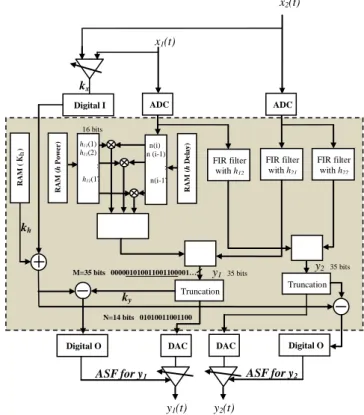
Fig. 1. Principle scheme using ASF.
y1 35 bits y2 35 bits y1(t) y2(t) x1(t) ky ASFfor y1 kh M=35 bits 000001010011001100001… Truncation FIR filter with h12 R A M ( h P ow e r ) h11(1) h11(2) : h11(17) n(i) n (i-1) : n(i-17) R A M ( h D e lay) kx ADC R A M ( kh ) FIR filter with h21 FIR filter with h22 DAC Digital O Truncation ASFfor y2 Digital O Digital I DAC x2(t) ADC
International Journal of Research in Wireless Systems (IJRWS), Volume 2, Issue 29 (2013) 3 The coloured large block is the programmable digital part
(Virtex-IV) of the hardware simulator. “I” stands for Input and “O” for Output.
The maximum voltage supported by the Analogue-Digital Convertor (ADC) is 1 V. If x1 < 0.25 V, it is multiplied by
where is the integer verifying:
(1)
with (2)
where is the smallest integer greater than (or equal to) .
In the same way, If x2 < 0.25 V, it is multiplied by
where is the integer verifying:
(3)
with (4)
The input signal cannot exceed 1 V. Thus, we define by:
(5)
In fact, we cannot provide the digital input by and
because the ASF calculated and provided to the digital output will be unknown.
If hmax = max (|h|) < 0.5, it is be multiplied by where:
(6)
and (7)
is determined for every MIMO profile and it is saved in a RAM block in the FPGA. A gain controlled amplifier is placed
before the ADC to control and send it to the FPGA. Also,
controlling the power of x at a sampling period smaller than
the sampling period of the FPGA is not easy. Thus, is
provided for a package of x samples.
In the case of a brutal truncation, ASFbxh = , and
using just the ASF on h, ASFbh = . Moreover, a better
solution is the sliding truncation (used in Figure 1) that selects the most significant bits. This truncation scans the bits until it detects a “1” bit, then it considers the 14 bits just form the first “0” bit that stands before it. In fact the ADC and the Digital-Analogue convertor (DAC) have a resolution of 14 bits. In this case, if the output signals are presented on more than
14 bits, the sliding factor has to be considered to obtain
the correct output signal. Thus, ASF = , and
using just the ASF on h, ASFsh = . The resulting ASF is
sent to a gain controlled amplifier to restore the true value of the output signals, as presented in Figure 1.
The FPGA Virtex-IV has a limited number of digital outputs, thus the quantification of ASF is discussed in Section V.
IV. HARDWARE IMPLEMENTATION
Four FIR filters are used to implement a 2×2 MIMO channel. For TGn channel model B, each FIR filter has 9 DSP blocks (multipliers) which is equal to the number of taps of the impulse response. The Virtex-IV SX35 (described in [11]) prototyping board utilisation summary is given in Table I with the circuit used to reload the channel coefficients.
We have developed our own FIR filter instead of using Xilinx MAC filter to make it possible to reload the filter coefficients.
TABLE I.
VIRTEX-IV UTILISATION FOR MIMO 2×2 ASF-BASED
ARCHITECTURE
Logic Utilisation Used Available Utilisation Slice Flip Flops 1,615 30,720 5 %
4 input LUTs 2,556 30,720 8 % Occupied Slices 2,090 15,360 13 % Bonded IOBs 40 448 8 % BUFG/BUFGCTRLs 1 32 3 % FIFO16/RAMB16s 37 192 19 % DSP48s 36 192 18 %
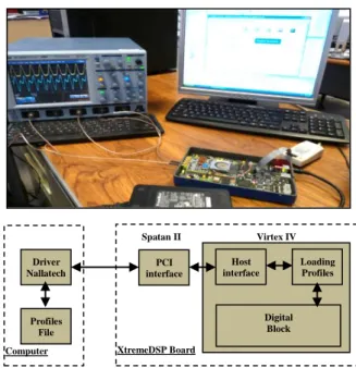
Figure 2 shows the connection between the computer and the FPGA board to reload the coefficients.
Fig. 2. Connection between the computer and the XtremeDSP board. Spatan II Virtex IV XtremeDSP Board Computer Driver Nallatech Profiles File PCI interface Digital Block Host interface Loading Profiles
AUTO-SCALE FACTOR ALGORYTHM FOR MIMO CHANNEL HARDWARE SIMULATOR: TOWARD HIGHER AND STABLE SNR
International Journal of Research in Wireless Systems (IJRWS), Volume 2, Issue 29 (2013) 4 For the test, 10000 successive profiles of a 2×2 MIMO
time-varying channel are considered. The refreshing frequency fref is chosen to be 15 Hz for v = 1.2 km/h. The
refreshing period is tref = 66.66 ms during which we must
refresh all of the four profiles, i.e. 9 taps × 4 FIR filters = 36 words of 16 bits = 72 bytes to transmit a MIMO profile, which is 72/tref = 1.08 kBps.
The PCI bus is chosen to load the profiles of the impulse responses. It has a speed of 30 MB/s. While a MIMO profile is used, the following MIMO profile is loaded and will be used after the refresh period.
The time domain architecture presented in [8] and [10] produces an occupation of 11 % to 13 % of slices on the FPGA for one SISO channel. However, the ASF-based architecture presents an occupation of 3 % for one SISO channel and 13 % for 2×2 MIMO channel.
V. ARCHITECTURE ACCURACY
In order to determine the accuracy, a comparison is made between theory/ Xilinx output signals. The input signals are considered the same for simplification: x(t) = x1(t) = x2(t). x is
considered Gaussian and it is quantified on 14 bits. It presents the two 2×2 MIMO channel inputs:
where fs = 165 MHz is the sampling frequency, Ts = 1/fs is the
sampling period, Wt = 250Ts, mx = 3 Wt/4 and = mx/4. The
ADC/DAC convertors have a full scale of [-Vm,Vm], with Vm = 1
V. We consider xm= Vm / 4 < Vm / 2 to test the ASF-based
architecture.
The theoretic output signals are:
To analyze the difference between the output signals, the relative error is computed for each output sample to by:
and the relative SNR by:
SNR = 20
Figure 3 presents a snapshot of the theory and the Xilinx output signals. yth1, yth2, yASF1 and yASF2 presents y1(t), y2(t),
Xilinx output 1 using ASF and Xilinx output 2 using ASF, respectively.
Fig. 3. Snapshot of the output signals.
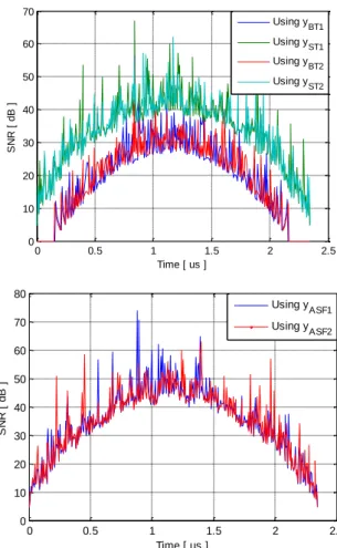
Figure 4 presents the relative SNR without using ASF and using ASF of the snapshot taken in Figure 2. BT stands for Brutal Truncation and ST for Sliding window Truncation.
Fig. 4. Output relative SNR without using ASF (left) and using ASF (right).
0 0.5 1 1.5 2 2.5 0 0.5 1 1.5 2 2.5 3 3.5 4 Time [ us ] y [ V ] yth1 yth2 yASF1 yASF2 0 0.5 1 1.5 2 2.5 0 10 20 30 40 50 60 70 Time [ us ] S N R [ d B ] Using yBT1 Using yST1 Using yBT2 Using yST2 0 0.5 1 1.5 2 2.5 0 10 20 30 40 50 60 70 80 Time [ us ] S N R [ d B ] Using y ASF1 Using y ASF2
International Journal of Research in Wireless Systems (IJRWS), Volume 2, Issue 29 (2013) 5 Figure 4 shows the benefit of using ST. Moreover, using
ASF provides a higher SNR. To present the results more clearly, the global values of the relative error and the SNR are necessary to evaluate the accuracy of the architectures. They are computed respectively by:
, (13)
where E = YXilinx - Yth is the error vector. The global SNR for all
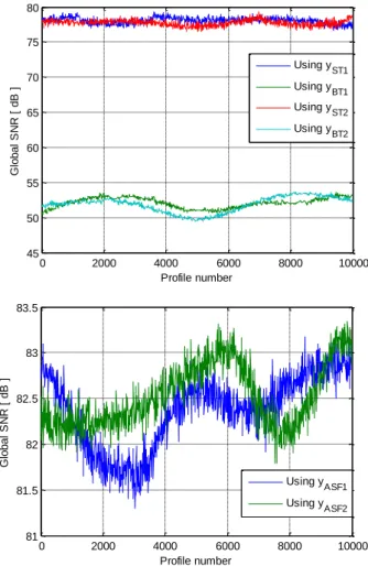
the MIMO profiles are presented in Fig 5.
Fig. 5. Global relative SNR for all the MIMO profiles without using ASF (left) and using ASF (right).
In Fig 5, the BT provides a global SNR that ranges between 49 and 54 dB. The ST provides a higher global SNR that ranges between 77 and 79 dB. However, using the ASF-based architecture, the global SNR ranges between 81 and 84 dB.
These values depend on the range of the attenuation of h that varies in time. In our case, it varies between -/+ 7 dB. In fact, the ASF-based architecture has more benefit if the attenuation of h increases.
Therefore, Fig 6 presents the effect of the ASF on the global output SNR versus the attenuation of h. Moreover, it
presents the variation of the parameters and versus
the attenuation of h.
a-
b-
Fig. 6. ASF effects versus the attenuation of h: a- The global SNR, b- ASF parameters.
A FPGA Virtex-IV provides 34 pin (external digital I/O) Adjacent Bus Header on the motherboard of the FPGA. This will provides 28 direct bi-directional connections to the main user FPGA. The remainder of the pins are No-Connects (NC)
pins. Thus, provided to the input of the FPGA and the two
ASF provided to the output y1 and y2 are quantified on 9 bits.
For high attenuation, the ASF increase the global SNR significantly. For ASFsh = – , it will be quantified on 18
bits instead of 9. In fact, in this case, the 9 bits specified for can be used. Thus, as shown in Fig 6, for an attenuation of
h higher than 15 dB, it is better to eliminate to obtain a higher and more stable output SNR. However, for an
attenuation of h lower than 15 dB, it is better to use and
attend an SNR of 100 dB. Also, the result shows the benefit of
the sliding truncation (ASFsh) on the brutal truncation (ASFbh).
0 2000 4000 6000 8000 10000 45 50 55 60 65 70 75 80 Profile number G lo b a l S N R [ d B ] Using y ST1 Using yBT1 Using y ST2 Using y BT2 0 2000 4000 6000 8000 10000 81 81.5 82 82.5 83 83.5 Profile number G lo b a l S N R [ d B ] Using y ASF1 Using y ASF2 0 5 10 15 20 25 30 0 10 20 30 40 50 60 70 80 90 100 h attenuation [ dB ] G lo b a l S N R [ d B ] ASF for y 1 ASF for y 2 ASF sh for y1 ASF sh for y2 ASF bh for y1 ASF bh for y2
W ithout ASF for y
1
W ithout ASF for y
2 0 5 10 15 20 25 30 0 2 4 6 8 h attenuation [ dB ] A S F p a ra m e te rs v a ri a ti o n k y1 before ASF k y2 before ASF k y1 using ASF k y2 using ASF k h
AUTO-SCALE FACTOR ALGORYTHM FOR MIMO CHANNEL HARDWARE SIMULATOR: TOWARD HIGHER AND STABLE SNR
International Journal of Research in Wireless Systems (IJRWS), Volume 2, Issue 29 (2013) 6 Table 2 shows the error/SNR mean global values for all
profiles using ST or BT with the ASF-based architecture and with a simple time domain architecture (without ASF).
TABLE II.
MEAN GLOBAL RELATIVE ERROR ( ) AND SNR .
With ASF Without ASF
(%) (dB) (%) (dB) y1 ST 0.0072 83.01 0.0132 77.65 BT 0.2661 51.67 0.4724 46.62 y2 ST 0.0072 82.88 0.0130 77.79 BT 0.2570 51.95 0.5064 46.01
The mean global SNR values show the benefit of using an ASF-based architecture. The SNR is increased by 5 dB compared to a time domain architecture using just ST, and by 37 dB compared to the simple time domain architecture using BT.
ACKNOWLEDGMENT
The authors would like to thank CEDRE for its financial support of this work.
REFERENCES
1. “Xilinx: FPGA, CPLD and EPP solutions”, www.xilinx.com. 2. P. Murphy, F. Lou, A. Sabharwal and P. Frantz, “An FPGA based
rapid prototyping platform for MIMO systems”, Asilomar Conf. on Signals, Systems and Computers, ACSSC, vol. 1, pp. 900-904, 9-12 Nov. 2003.
3. Erceg, V., Shumacher, L., Kyritsi, P., et al.: “TGn Channel Models”, IEEE 802.11- 03/940r4, May 10, 2004.
4. “Advanced design system – LTE channel model - R4-070872 3GPP TR 36.803 v0.3.0”, Agilent Technologies, 2008.
5. H. Farhat, R. Cosquer, G. Grunfelder, L. Le Coq and G. El Zein, “A dual band MIMO channel sounder at 2.2 and 3.5 GHz”, IMTC, Victoria, BC, Canada, May 2008.
6. P. Almers, E. Bonek et al., “Survery of channel and Radio propagation models for wireless MIMO systems”, EURASIP Journal on Wireless Communications and Networking, Article ID 19070, 2007.
7. L. Schumacher, K. I. Pedersen and P.E. Mogensen, “From antenna spacings to theoretical capacities – guidelines for simulating MIMO systems”, in Proc. PIMRC Conf., vol. 2, pp. 587-592, Sep. 2002.
8. S. Picol, G. Zaharia, D. Houzet and G. El Zein, “Hardware simulator for MIMO radio channels: design and features of the digital block”, IEEE VTC Fall, Calgary, Canada, Sep. 2008. 9. S. FouladiFard, A. Alimohammad, B. Cockburn and C. Schlegel,
“A single FPGA filter-based multipath fading emulator”, Globecom, Honolulu, Nov. 2009.
10. H. Eslami, S.V. Tran and A.M. Eltawil, “Design and implementation of a scalable channel Emulator for wideband MIMO systems”, IEEE Trans. on Vehicular Technology, vol. 58, no. 9, pp. 4698-4708, Nov. 2009.
11. B. Habib, G. Zaharia and G. El Zein, “MIMO hardware simulator: new digital block design in frequency domain for streaming signals”, Journal of Wireless Networking and Comm., vol. 2, no. 4, pp. 55-65, 2012.
12. B. Habib, H. Farhat, G. Zaharia and G. El Zein, “Hardware Simulator Design for MIMO Propagation Channel on Shipboard at 2.2 GHz”, Wireless Personal Communications, Springer, DOI 10.1007/s11277-012-0954-2, 2012.
13. B. Habib, G. Zaharia and G. El Zein, “Digital block design of MIMO hardware simulator for LTE applications”, ICC, Ottawa, Canada, 2012.
14. “Wireless Channel Emulator”, Spirent Communications, 2006. 15. Telecommunications solutions, testing solutions, and
automated systems for the wireless industry”, Elektrobit, 1999.
International Journal of Research in Wireless Systems (IJRWS), Volume 2, Issue 29 (2013) 7
Bachir Habib is currently a PhD student on telecommunication at IETR/INSA Rennes, France. He is a PhD student’s representative at Matisse. His research
interests include Hardware Simulators design for radio propagation environments. He is a session chair at ICC 2012. He received the Master degree in telecommunication from the National Institute of Applied Sciences of Rennes, France.
Gheorghe Zaharia received the B.S. degree in electronics and telecommunications from the Polytechnic Institute of Iasi, Romania, in 1981 and the D.E.A. and
Ph.D. degrees in telecommunications, signal processing and electronics from the “Institut National des Sciences Appliquées » (INSA) of Rennes, France, in 1991 and 1997, respectively.
From 1983 to 1990 he was a Lecturer at the Technical University of Iasi. Between 1983 and 1985 he studied mathematics at the University “Al. I. Cuza” of Iasi. Since 1997, he is Associate Professor in the Department “Communications Systems and Networks”, the former “Electronics and Communications Systems” Department, INSA, Rennes. His teaching and research interests mainly concern the study of radio waves propagation, communications systems, information theory, and coding. Gheorghe Zaharia is Senior Member IEEE and member of the Romanian Society of Medical Bioengineering.
Ghais El Zein received the M.S. degree in Electronics, the Ph.D. degree in Telecommunications and Signal Processing, and the H.D.R. “Habilitation à Diriger des
Recherches” degree in Electronics from the University of Rennes 1 - France, in 1983, 1988 and 1998, respectively. From 1985 to 1987, he was a Lecturer, and from 1990 to 1999, an Associate Professor, in the Department of Electronics and Communications Systems Engineering, of the “Institut National des Sciences Appliquées de Rennes” (INSA) - France, where he is currently a Professor. His teaching and research interests mainly concern the study of radiowave propagation phenomena and the evaluation of their effects on communication systems. From 2001 to 2009, he served as deputy director of the Institute of Electronics and Telecommunications of Rennes (IETR - UMR CNRS 6164). Since 2009, he is the Head of Radio Propagation Team. He is a member of URSI-F and member of the Monitoring and Assessment Committee (CSE) of the “Images et Réseaux” cluster. Since 2011, he is responsible for the Master I-MARS