HIGH-LEVEL MODELLING OF OPTICAL INTEGRATED NETWORKS-BASED SYSTEMS WITH THE PROVISION OF A LOW LATENCY CONTROLLER
FELIPE GOHRING DE MAGALHÃES
DÉPARTEMENT DE GÉNIE INFORMATIQUE ET GÉNIE LOGICIEL ÉCOLE POLYTECHNIQUE DE MONTRÉAL
THÈSE PRÉSENTÉE EN VUE DE L’OBTENTION DU DIPLÔME DE PHILOSOPHIÆ DOCTOR
(GÉNIE INFORMATIQUE) MAI 2017
c
ÉCOLE POLYTECHNIQUE DE MONTRÉAL
Cette thèse intitulée:
HIGH-LEVEL MODELLING OF OPTICAL INTEGRATED NETWORKS-BASED SYSTEMS WITH THE PROVISION OF A LOW LATENCY CONTROLLER
présentée par: GOHRING DE MAGALHÃES Felipe en vue de l’obtention du diplôme de: Philosophiæ Doctor a été dûment acceptée par le jury d’examen constitué de:
Mme BOUCHENEB Hanifa, Doctorat, présidente
Mme NICOLESCU Gabriela, Doctorat, membre et directrice de recherche M. HESSEL Fabiano, Ph.D., membre et codirecteur de recherche
Mme LIBOIRON-LADOUCEUR Odile, Ph.D., membre et codirectrice de recherche M. BELTRAME Giovanni, Ph.D., membre
DEDICATORY
ACKNOWLEDGMENTS
First, I would like to thank my wife Val, for the support and friendship. Thanks for staying awake in working late hours and drinking chimarrão with me, so we could stay awake. Thank you for the period abroad in the cold Montreal, your presence made everything easier. Thank you for everything.
A special thanks to my advisors, Professor Fabiano, Professor Gabriela and Professor Odile, for the guidance and patience (specially the patience!). Without your instructions I would never have gone this far.
Thanks to all the friends made along the way, in Brazil and Canada. The discussions brought different views and enriched this project.
RÉSUMÉ
La tendance du marché dans la conception des architectures multiprocesseurs de la prochaine génération consiste à intégrer de plus en plus de cœurs dans la même puce. Cette concentra-tion des cœurs dans la même puce exige l’amélioraconcentra-tion des politiques d’intercommunicaconcentra-tion. L’une des solutions proposées dans ce contexte consiste à utiliser les réseaux sur puce vu qu’ils présentent une amélioration considérable en termes de la bande passante, l’évolutivité et de l’extensibilité. Néanmoins, vu la croissance exponentielle en nombres de cœurs sur puce, les interconnexions électriques dans les réseaux sur puce peuvent devenir un goulet d’étranglement dans la performance du système. Par conséquent, des nouvelles techniques et technologies doivent être adoptées pour remédier à ces problèmes.
Les réseaux optiques intégrés (OIN venant de l’anglais Optical Integrated Networks) sont actuellement considérés comme l’un des paradigmes les plus prometteurs dans ce contexte. Les OINs offrent une plus grande bande passante, une plus faible consommation d’énergie et moins de latence lors de l’échange des données. Plusieurs travaux récents démontrent la faisabilité des OIN avec les technologies de fabrication disponibles et compatibles avec CMOS. Cependant, les concepteurs des OINs font face à plusieurs défis :
• Actuellement, les contrôleurs représentent le principal goulot d’étranglement de la com-munication et présentent l’un des facteurs minimisant l’efficacité des OINs. Alors, la proposition des nouvelles solutions de contrôle à faible latence est de plus en plus pri-mordiale pour en tirer profit.
• Le manque d’outils de modélisation et de validation des OINs. La plupart des travaux se concentrent sur la conception des dispositifs et l’amélioration des performances des composants de base, tout en laissant le système sans assistance.
Dans ce contexte, afin de faciliter le déploiement de systèmes basés sur les OINs, cette thèse se focalise sur les trois contributions majeures suivantes: (1) le développement d’un ensemble de méthodes précises de modélisation qui va permettre par la suite de réaliser une plateforme de simulation au niveau du système ; (2) la définition et le développement d’une approche de contrôle efficace pour les systèmes basés sur les OINs; (3) l’évaluation de l’approche de contrôle proposée.
ABSTRACT
Design trends for next-generation Multi-Processor Systems point to the integration of a large number of processing cores, requiring high-performance interconnects. One solution being applied to improve the communication infrastructure in such systems is the usage of Networks-on-Chip as they present considerable improvement in the bandwidth and scaleabil-ity. Still as the number of integrated cores continues to increase and the system scales, the metallic interconnects in Networks-on-Chip can become a performance bottleneck. As a result, a new strategy must be adopted in order for those issues to be remedied.
Optical Integrated Networks (OINs) are currently considered to be one of the most promising paradigm in this design context: they present higher bandwidth, lower power consumption and lower latency to broadcast information. Also, the latest work demonstrates the feasibility of OINs with their fabrication technologies being available and CMOS compatible.
However, OINs’ designers face several challenges:
• Currently, controllers represent the main communication bottleneck and are one of the factors limiting the usage of OINs. Therefore, new controlling solutions with low latency are required.
• Designers lack tools to model and validate OINs. Most research nowadays is focused on designing devices and improving basic components performance, leaving system unattended.
In this context, in order to ease the deployment of OIN-based systems, this PhD project focuses on three main contributions: (1) the development of accurate system-level modelling study to realize a system-level simulation platform; (2) the definition and development of an efficient control approach for OIN-based systems, and; (3) the system-level evaluation of the proposed control approach using the defined modelling.
TABLE OF CONTENTS
DEDICATORY . . . iii
ACKNOWLEDGMENTS . . . iv
RÉSUMÉ . . . v
ABSTRACT . . . vi
TABLE OF CONTENTS . . . vii
LIST OF TABLES . . . x
LIST OF FIGURES . . . xi
LIST OF ACRONYMS AND ABBREVIATIONS . . . xiv
LIST OF ANNEXES . . . xvi
CHAPTER 1 INTRODUCTION . . . 1
1.1 Context and Motivations . . . 1
1.2 Objectives & Contributions . . . 3
1.3 Document Organization . . . 3
CHAPTER 2 BASIC CONCEPTS . . . 5
2.1 Basic Concepts Related to Optical Interconnects . . . 5
2.1.1 Mach-Zehnder Interferometer . . . 8
2.1.2 Micro-Ring Resonator . . . 10
2.1.3 Optical Integrated Networks . . . 11
2.2 Control Unit . . . 15
2.2.1 Time Sharing . . . 15
2.2.2 Dynamically Paths Setting . . . 17
2.2.3 Wavelength Division . . . 18
2.3 High-level Modelling Strategies and Description Languages . . . 18
CHAPTER 3 RELATED WORK . . . 22
3.1.1 Industrial Tools . . . 22 3.1.2 Academic Tools . . . 23 3.2 Controlling Schemes . . . 25 CHAPTER 4 METHODOLOGY . . . 31 4.1 Methodology Overview . . . 31 4.2 High-level Modelling . . . 33
4.3 Control Unit Design . . . 35
4.4 Validation Architectures . . . 41
4.4.1 Switches . . . 41
4.4.2 Topologies . . . 43
CHAPTER 5 CONTROL UNIT - THE LUCC . . . 45
5.1 Path Analyzer and LUT Creation - The PALC . . . 48
5.2 Conflict Resolution Block - The CRB . . . 53
5.3 Dynamic Setup Block . . . 55
5.4 Discussion . . . 57
CHAPTER 6 CONTROL UNIT - THE HYCO . . . 59
6.1 Conflict Resolution Unit . . . 61
6.2 Bloom Filter . . . 63
6.3 Access Control Unit (ACU) . . . 68
6.4 Distributed Configuration Unit (DCU) . . . 68
6.5 Discussion . . . 70
6.5.1 HyCo and LUCC Comparison . . . 71
CHAPTER 7 SIMULATION PLATFORM - THE SF-SIM . . . 72
7.1 Discussion . . . 76
CHAPTER 8 RESULTS . . . 78
8.1 LUCC Execution Results . . . 78
8.1.1 LUCC Simulation . . . 80
8.1.2 LUCC Prototyping in Xilinx FPGA . . . 82
8.1.3 LUCC Prototyping in Altera FPGA . . . 82
8.2 Co-Design of the Control Unit and the Optical Switch . . . 83
8.3 Models Integration . . . 89
8.4 HyCo Execution Results . . . 94
8.6 Controllers Comparison . . . 97 CHAPTER 9 CONCLUSION . . . 100 9.1 Final Remarks . . . 100 9.2 Future Work . . . 101 REFERENCES . . . 102 ANNEXES . . . 112
LIST OF TABLES
Table 3.1 Tools Comparison . . . 25
Table 3.2 Controlling solutions comparison . . . 29
Table 4.1 Adjacency matrix examples. The left matrix represents the SF 8×8 network, while the right matrix represents the Spidergon 8×8 network. 36 Table 5.1 LUT Growing Size. . . 55
Table 6.1 Bloom filter bit array initial state. . . 63
Table 6.2 Updated Bloom filter bit array with positions 12 and 6 marked to ’1’. 63 Table 6.3 Updated Bloom filter bit array with positions 1 and 10 marked to ’1’. 64 Table 6.4 Bloom filter bit array testing example for input = 225. . . 64
Table 6.5 Bloom filter bit array testing example for input = 161. . . 65
Table 8.1 Configuration parameters for the 2×2 switch. . . 91
Table 8.2 Simulation times for different topologies. . . 94
Table 8.3 Simulation accuracy comparison. . . 94
Table 8.4 Synthesis values for the Virtex V 330T Xilinx FPGA . . . 96
Table 8.5 Synthesis values for the Stratix IV Altera FPGA . . . 97
Table 8.6 Synthesis values for the 65nm STMicro Library . . . 97
LIST OF FIGURES
Figure 2.1 Waveguides Examples. . . 6
Figure 2.2 Insertion loss Overview. . . 7
Figure 2.3 Crosstalk example of a ring resonator. . . 8
Figure 2.4 Shift phase example. . . 9
Figure 2.5 Mach-Zehnder Interferometer. . . 9
Figure 2.6 2×2 MZI-based integrated switch. . . 10
Figure 2.7 Example of a filter using MR. . . 11
Figure 2.8 1x2 Basic switch using one MR. . . 12
Figure 2.9 SERDES block exemplification. . . 14
Figure 2.10 Organizational Example of OIN-based System. . . 14
Figure 2.11 Resource Sharing System Example. . . 16
Figure 2.12 System overview using a centralized time-sharing-based control unit. . 16
Figure 2.13 System Overview Using a Distributed Circuit-switching-based Control Unit . . . 17
Figure 2.14 System Overview Using a Centralized frequency-division-based Control Unit. . . 18
Figure 2.15 Design Abstraction Levels . . . 20
Figure 4.1 OIN-based system modelling iterative methodology. . . 33
Figure 4.2 Controller Design Overview. . . 35
Figure 4.3 Controller Design Overview. . . 36
Figure 4.4 LUT growing size exemplification. . . 38
Figure 4.5 Graph representation of a 2×2 MZI-based optical switch. . . 39
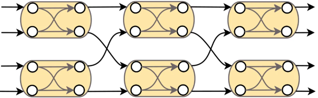
Figure 4.6 Graph representation of a 4×4 MZI-based Beneš optical switch. . . . 39
Figure 4.7 Internal architecture of a 4×4 MZI-based Spanke-Beneš optical switch. 40 Figure 4.8 Internal architecture of a 4×4 MZI-based strictly non-blocking optical switch. . . 40
Figure 4.9 Internal architecture of an 8×8 Beneš network based on employing several 2×2 and 4×4 optical switches . . . 41
Figure 4.10 2×2 Validation Switch. . . 42
Figure 4.11 4×4 validation topologies. . . 42
Figure 4.12 5×5 Validation Switch. . . 43
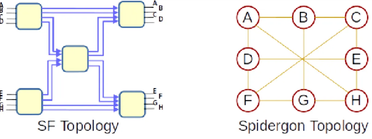
Figure 4.13 8x8 SF Network . . . 44
Figure 5.2 iSLIP throughput X iterations number. . . 47
Figure 5.3 LUCC decision flow chart. . . 48
Figure 5.4 8×8 Beneš topology numbered graph representation. . . 50
Figure 5.5 Graph view of 8×8 SF Network. . . 57
Figure 6.1 HyCo overview. . . 59
Figure 6.2 Hybrid Controller execution flow. . . 60
Figure 6.3 Conflict detection and Round-Robin execution flow. . . 62
Figure 6.4 Bloom filter block execution example. . . 67
Figure 6.5 Access control unit simplified execution exemplification. . . 69
Figure 6.6 DCU Distribution approach. . . 70
Figure 7.1 Simulation platform. . . 72
Figure 7.2 2×2 modelled switch. . . 73
Figure 7.3 2×2 MZI-based Switch simulation. . . 73
Figure 7.4 4×4 MZI-based Beneš switch. . . 74
Figure 7.5 4×4 MZI-based Switch simulation . . . 74
Figure 7.6 8×8 SF Network Simulation . . . 75
Figure 7.7 SF-Sim Configuration Window. . . 76
Figure 7.8 4×4 Example topology on DIA tool. . . 77
Figure 8.1 Traffic patterns exemplification. . . 79
Figure 8.2 LUCC Simulation for 4×4 Beneš topology. . . 81
Figure 8.3 LUCC Simulation for 8×8 SF topology. . . 81
Figure 8.4 LUCC Xilinx FPGA execution. . . 82
Figure 8.5 LUCC on Altera FPGA execution. . . 83
Figure 8.6 Microscopic picture of the 4×4 MZI-based switch. . . 84
Figure 8.7 Schematic of the lab setup for the opto-electrical co-design. . . 84
Figure 8.8 Measured 10 Gb/s PRBS31 signal switched by the 2×2 MZI switch. . 85
Figure 8.9 Lab-setup overview . . . 86
Figure 8.10 FPGA and Optical Switch Readings. . . 87
Figure 8.11 Complete System Lab Setup Overview. . . 88
Figure 8.12 Online Readings of Prototyped Optical Switch and FPGA Execution. 89 Figure 8.13 Extracted data from second set of lab experiments . . . 90
Figure 8.14 4×4 Spanke-Beneš Simulation Scenarios. . . 91
Figure 8.15 4×4 Spanke-Beneš simulation. . . 92
Figure 8.16 System Simulation Setup. . . 93
Figure 8.17 System simulation output. . . 93
Figure 8.19 Latency comparison between controllers and state-of-the-art. . . 98
Figure A.1 2×2 Switch Block Overview. . . 113
Figure A.2 2×2 Switch Output Selection Logic . . . 114
Figure A.3 Logical Block Of Described 2×2 MZI-based Switch . . . 115
Figure A.4 SF-Sim GUI Configuration Window. . . 117
Figure A.5 SF-Sim GUI MZI Configuration Window. . . 118
Figure A.6 SF-Sim GUI DIA Configuration Window. . . 119
Figure A.7 SF-Sim GUI DIA Workbench. . . 120
Figure A.8 SF-Sim GUI DIA Workbench Presenting Connected Nodes. . . 120
Figure A.9 SF-Sim GUI DIA Workbench I/O Nodes Placement. . . 121
Figure A.10 SF-Sim GUI DIA Workbench I/O Nodes Colouring. . . 121
LIST OF ACRONYMS AND ABBREVIATIONS
ADL Architecture Description Language
CMOS Complementary Metal-Oxide-Semiconductor CMP Chip Multiprocessor
CRB Conflict Resolution Block DSB Dynamic Setup Block eNOC Electrical Network-on-chip FIFO First-in-first-out
FLB FPGA logical blocks FSM Finite-state-machine Gbps Gigabits per second GUI Graphical User Interface
HDL Hardware Description Languages HYCO Hybrid Controller
I/O Input-and-Output IoT Internet of Things IP Intelectual Property
LUCC LUT-based Centralized Controller LUT Look-Up Table
MR Micro-ring Resonator
MZI Mach-Zehnder Interferometer NI Network-Interface
OINs Optical Integrated Networks ONOC Optical Network-on-Chip P2P Point-to-Point
PICS Photonic Integrated Circuits
RR Round-Robin
RTL Register transfer level SERDES Serializer/Deserializer SF-Sim Straight-forward Simulator SF StraightForward
SNR Signal-to-noise Ratio SOI Silicon-on-Insulator SPF Shortest Path First
TDM Time Division Multiplexing UML Unified Modelling Language
VHDL VHSIC Hardware Description Language WBA Weight Based Arbiter
WDM Wavelength-division multiplexing XUP Xilinx University Program
LIST OF ANNEXES
CHAPTER 1 INTRODUCTION
This chapter includes an overview of the motivations, objectives, and the proposed contri-butions in the field of optical integrated networks modelling and controlling. The context of optical networks and the research challenges that inspired this thesis are introduced and deployed solutions to address the challenges are shortly commented. Lastly, the document organization is presented.
1.1 Context and Motivations
Nowadays systems present a rising number of features, leading to a significant growth in the applications’ design complexity. Mostly, these systems have their implementation based on multiple processing elements integrated on the same die and running at a lower clock frequency due to energy consumption constraints [1].
Since the introduction of Chip Multiprocessor (CMP), one of the design main concerns lies in how the communication among internal components is performed. Bus-based systems present a well-known solution with a reasonable bandwidth and great ease of implementation. As the number of components rises, the complexity of bus design increases and their application becomes challenging [2]. Moreover, the communication can become a bottleneck in the system performance of traditional bus-based systems, which can compromise its operation [3]. Aiming to solve this issue, Electrical Network-on-Chip (eNoC) is one of the most popular solutions that have been proposed.
Systems based on eNoCs tend to provide better communication performance [4] when com-pared to traditional bus-based systems. In this case, the communication management is performed by routers that forward packets through the network. Each network node con-sists of a router and a connected component which could be, for example, a processor or a memory. Besides the gain in the communication capability, eNoCs usually present improved energy reliability and efficiency as well as high re-usability [5]. However, as the number of possible integrated cores on a single chip continues to increase, metallic interconnects in eNoCs will become a bottleneck due to their high power consumption, limited bandwidth, long latency and poor scaleability, leading ITRS [6] to point out the need for a new tech-nology to overcome such restrictions. Another drawback of employing eNoCs is related to their architectural organization. As eNoCs rely on point-to-point communication links, their usage might be limited as the system scales, resulting in higher contention for long-distance
communications among cores and consequently performance degradation through imposing a higher power consumption. In this design context, Optical Integrated Networks (OINs) and the 3D die stacking1 are currently considered to be the two most promising new paradigms [7–11].
OINs are already a reality for long-distance communications [12] and their usage for short-distance communications, such as inter-chip communications, has already been proven to be applicable [13, 14]. Recently, published work presented photonic architectures with low power consumption, low insertion loss and low power penalty [15, 16]. These work bring forward OINs as attractive candidates for high demanding communicating architectures. Optical Network-on-chip (ONoC) emerges as a possible solution to overcome the aforemen-tioned eNoCs issues as it presents a higher bandwidth when compared to common electrical eNoCs implementations with low power consumption [17]. Also, another advantage of em-ploying ONoCs lies on their own physical implementation. With eNoCs, communications are usually local (Point-to-Point - P2P), reducing their design complexity but not allowing good scaleability for shared resources. On the other hand, ONoCs present a potential support for broadcasting messages, making them suitable for the new multiprocessors paradigms [18]. The performance and efficiency of such architectures are constrained by their controllers. The control part has an important impact on the OIN overall performance and a better solution is yet to be found [19]. Previous works demonstrated architectures with either long setup time or that have become too complex, thus challenging practical deployment [20, 21]. Consequently, while low latency controllers have been demonstrated [22, 23], further improvement in their response time is still required to realize practical deployment of OINs. Further, most proposed controllers are deeply attached to the network for which they are designed. Although this fact may lead to an increase in the performance of the controller, this goes against the trend for the next generation of communication systems, in which it is believed that each network layer (application, control and physical) will be independent from each other [24, 25]. Designing a system based on OINs is a very complex task that need to be automated using efficient tools. While the device level presents indeed a dense support in terms of automation tools for the development of optical devices, this is not true for the system level. In fact, when compared with high-level electrical design tools, system level support is nearly nonexistent [6]. Acknowledging the importance of this aspect, it is important to highlight that it is not possible to design an entire system with nowadays commercial tools, as it would be a complex 13D die stacking is an integrated circuit manufacturing technique in which two or more silicon wafers are
placed one over the other and interconnected vertically using through silicon via (TSVs) in such a way that they behave as a single device. This technique is key in the OINs dissemination as it allows the integration of a variety of technologies prototyped onto the same chip.
task and would need more advanced tools. So, a research gap is open for the development of methods and tools to aid in the design of OIN-based systems.
Aforementioned issues raise two important questions to be addressed by researchers: (i) how to better explore system-level design of OIN-based systems , and; (ii) how to control OIN-based systems without adding prohibitive overhead to the system.
1.2 Objectives & Contributions
The main objectives of this thesis are:
1. Introducing an efficient solution to help designers better explore the design space for sys-tems integrating optical networks by finding the most promising solutions. This is achieved by providing a modelling strategy that is (i) complete, comprising all important characteris-tics of such systems; (ii) flexible, so it can describe any type of system; (iii) accurate, so the results extracted using it are close to real system implementations, and; (iv) not complex, so the modelling of systems does not impose a prohibitive an overhead during their deployment. 2. Developing efficient control solutions for OINs. The definition of a general solution for controlling OINs with a low-latency solution, that is flexible, in this way being able to deal with most kinds of optical networks and has a low overhead in time, thus not adding many extra clock cycles to compute requests and set dynamic configurations.
By fulfilling these objectives, we realize three main contributions:
1. The definition of accurate system-level modelling method enabling the development of a system-level simulation platform;
2. The definition and development of efficient control approaches for OIN-based systems, and;
3. The system-level evaluation of the proposed control approaches using the defined mod-elling methods.
1.3 Document Organization
This document is organized as follows. Next chapter presents basic concepts about photonic devices and networks as well as control techniques usually applied on such networks. Chapter 3 brings a state-of-the-art revision, positioning our approach with existing works. Chapter 4 gives first the global overview of the approach we defined for system-level design of OINs
and presents the proposed accurate system-level modelling methods. Following, Chapter 5 introduces the centralized control unit, employing Look-Up tables (LUT) in order to speed-up the control unit. Chapter 6 presents the hybrid controller developed, which relies on a centralized core and distributed units to reduce the control latency. Chapter 7 brings the simulation platform developed using introduced description models. Following, chapter 8 presents obtained results for both deployed controllers, the simulator accuracy as well as the models integration outcome. Finally, chapter 9 draws the conclusion of this document, along with the possible future work in the field.
CHAPTER 2 BASIC CONCEPTS
This chapter presents general concepts about optical components and systems, their control schemes as well as modelling techniques required to describe them. Section 2.1 covers topics such as waveguides, insertion loss and optical filters, from integration with complementary metal-oxide-semiconductor (CMOS) technology perspective. Section 2.2 discusses controlling solutions for OIN-based systems. Finally, section 2.3 brings an introduction to modelling and description concepts on the scope of multi-processed systems.
2.1 Basic Concepts Related to Optical Interconnects
Optical interconnects are well known for their capacity to transfer data with high transmission rates. On the opposite of their electrical counterpart, optical interconnects use light over an optical via to transmit information instead of wires. In order to take advantage of the maturity of the CMOS manufacturing technology, Silicon is the material of choice in order to deploy integrated optics [26]. One approach used is Silicon-on-Insulator (SOI). The SOI substrate is made of a thin silicon top layer separated from the silicon substrate by a buried oxide layer. The strong refractive index contrast between the core and the cladding material of the waveguide allows the realization of very compact components [27]. Other approaches are also possible, such as doped silica [28], silicon nitride [29] or silicon oxynitride on oxide [30]. Also, it is possible to separate the manufacturing of the electrical and optical circuits. In this case, the devices are made on different wafers, but still relying on the same materials mentioned before and then later bonded. In this thesis, we employ SOI fabrication technology as reference.
All optical devices are composed of some basic structures:
• A via is the path where the lights travel on, being the equivalent of wires in electrical devices;
• An interface is used to input data on the via or read/receive data to/from the via, and;
• Active and passive components are responsible for the control of the data flow on the device working like a filter. Passive components are static, while active components can be dynamic. Both types are detailed in Subsection 2.1.3.
An optical via is called a waveguide and is the path on which the light travels, usually with a rectangular structure. Nowadays, designs are projected with a waveguide width greater or equal to 450 nm and, as the size changes, different wavelengths might be transmitted on it. Different wavelengths might be used at the same time on the same waveguide transmitting data in parallel, provided that the waveguide supports these wavelengths. It is important to highlight that simultaneous connections are one of the main advantages of optical intercon-nections when compared to electrical-based ones.
As previously mentioned, waveguides are the paths on which light travels, and they should be as straight as possible to allow better transmission quality. However, it is nearly impossible to have a system composed exclusively by straight lines, being necessary to bend the waveguides in order for the light to change its direction. This is a crucial design step, as light might be completely lost in a very abrupt bend. Also, despite the fact that this may introduce a given signal loss, waveguides might cross each other without causing a non-functional state of the system, like it would in electrical crossing.
Figure 2.1 shows the three main types of waveguides: (a): straight waveguide, transmitting from one side to the other, exclusively; (b): crossing waveguides, where two inputs and two outputs can coexist, and; (c): waveguide bending, changing the transmission direction.
Figure 2.1 Waveguides examples (a) straight waveguide, (b) crossing waveguides and (c) waveguide bending.
When using optical components, one important aspect to be considered is the system in-sertion loss, which directly affects the power required for an input to reach its output. So, the higher the insertion loss, the higher is the power needed on the input. Each component introduces a given loss on the input signal, represented in Figure 2.2.
Figure 2.2 Insertion loss overview.
Additionally, total optical loss can be expressed as the sum of internal losses, in decibels (dB)
1
LossT OT AL = Lossinput+ Lossbending+ Lossw+ Lossoutput (2.1)
where Lossinput is the loss of the input signal when it couples into the waveguide, Lossbending
is the bending loss, Lossw is the waveguide loss, and Lossoutput is the loss of the output [31].
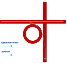
Another important effect to be studied and understood is the crosstalk. This happens when part of the signal couples on different waveguides, and it is not desired to happen. Figure 2.3 presents an example of crosstalk in a ring resonator, where it is possible to see the signal being transmitted from left to right, with the undesired fact that part of it is being coupled on the ring and going to the output on the bottom. This kind of issue introduces noise on the communication, which reduces the transmission quality and may jeopardize the reliability of the output signal. This is a risky situation because, sometimes, so much noise is inserted on the channel that is not possible to distinguish if the output signal is real data or only noise. Most designs focus on reducing both the insertion loss and crosstalk in order to obtain a more efficient architecture, with a better Signal-to-noise Ratio (SNR) [32]. SNR is a value that compares the relation of a noise signal to the desired signal over a component. This means that higher the ratio is, higher the transmitted signal quality is.
It is not possible to build an entire system relying solely on waveguides, as it would be nec-essary to create dedicated links for all possible communication paths, which is not feasible. 1Decibel indicates the proportion of a physical quantity in relation to an entry point. In other words,
decibels express a power ratio, not an amount. The simple equation which defines a decibel is: A = 10 ∗
log10P 2P 1(dB), where P1 is the power being measured, and P1 is the reference to which P2 is being compared.
The conversion from decibels measure back to power ratio is given by:P 2P 1 = 10( A10). For instance, the ratio of 1 kW to 1W, in decibels is: GdB = 10 ∗ log10(10001 ) = 30 dB.
Figure 2.3 Crosstalk example of a ring resonator, showing a portion of the signal being transmitted by the undesired waveguide.
This creates the need for more elaborated components, such as the Mach-Zehnder Inter-ferometer and Micro-Ring Resonator. These components incorporate extra functionalities, enabling the flow control in the network, working as network switches. Both components are presented in detail hereafter.
2.1.1 Mach-Zehnder Interferometer
A Mach-Zehnder Interferometer (MZI) is a device used to control the amplitude of an optical wave by dividing it in two, applying a given delay and then merging the two beans of light into one again. The physical implementation of such functionality works as it follows: the inserted wave is split in two, maintaining the same phase and amplitude for both resultant waves. One wave is transmitted over a straight waveguide and keeps its phase and amplitude. The second wave is somehow delayed, which inserts a phase change. Wave phase can be defined as the position of a wave point in one specific time. When a phase change happens, it means that the wave moved in time. Figure 2.4 illustrates this event, where two sinusoidal waves are presented. As it is possible to see, one sinusoidal wave is slightly forward in the X axis, which represents time. This can be defined as a phase change. By the time both waves are merged, the two waves can interfere constructively or destructively at the output. Depending on the interference, the introduced phase change affects the amplitude of the resultant wave [33].
For the shift phase, two approaches might be used: one active and one passive (the concepts of active and passive devices are covered in Subsection 2.1.3). Figure 2.5 presents the basic structure of one MZI, where it is possible to see the presence of two parallel waveguides, one
Amplitude
Time
Figure 2.4 Shift phase example, showing a sine wave changing its phase, thus moving in time.
with a delay portion and one as a straight line. In the image, it is possible to see an input signal being split in two, so they can travel each on their own waveguide, being later merged into one signal, on the output.
Figure 2.5 Mach-Zehnder Interferometer example structure.
For the delay that introduces the phase shift to be applied to the wave, we can use either an active or a passive device, as previously mentioned. For the active device an electrical arm is attached to the waveguide and a given current is applied to it. Depending on the applied current a different phase shift is induced. For the passive counterpart the phase shift is fixed at design time and may never change, being achieved by adding a series of waveguide bends in order to change the phase.
In order to build a MZI-based switch, two inputs and two outputs are employed. The light is split in the two arms of the input coupler of the interferometer, and they are later recombined in the output coupler of the interferometer. The switching between the ports is achieved by an electro-optic effect within the structure. Voltage, applied to the electrodes deposited on the integrated MZI, alters the electric field distribution within the substrate, which consequently changes its refractive index. By changing the effective refractive indices of one of the arms, it is possible to generate the phase difference between the optical signals in two arms of MZI. Based on the generated phase difference, the light switches from one output port to the other.
The following equations are used in order to determine the normalized power in each output port, where ∆φ is the difference of two phase changes [34].
Pout1 = sin2( ∆φ 2 ); (2.2) Pout2 = cos2( ∆φ 2 ); (2.3)
Figure 2.6 illustrates the 2×2 MZI-based integrated switch, where the input and output ports, the splitters and the integrated electrodes are presented.
Figure 2.6 2×2 MZI-based integrated switch structure.
2.1.2 Micro-Ring Resonator
A Micro-ring Resonator (MR) is an optical filter applied to select a desired wavelength from a given input and redirect it to an output [35]. On opposite to the presented MZI, MRs are wavelength selective. The MRs work based on three principles: optical coupling, total internal reflection, and constructive interference.
Total internal reflection is an effect in which the light travelling within a waveguide remains in the waveguide. It happens when the light hits the boundary of the waveguide and does not refract over the boundary. Constructive interference is when two waves interfere on each other and the resultant wave is the sum of the two interfering waves. Optical coupling is the effect of light travelling from one media to another. Particularly in MRs, it is the effect of the light travelling from the waveguide to the ring and from the ring to the waveguide. Three characteristics affect the optical coupling: the distance between the ring and the waveguide, the length of the coupling region and the refractive indexes2 of the waveguide and the ring. To 2The refractive index of a component is a constant that indicates how much the light will bend, or refract,
in that medium. It is defined by n = vc, where c is the speed of light, in vacuum and v is the phase velocity. For instance, the refractive index of silicon is 3.42, meaning that light travels 3.42 times faster in a vacuum
optimize the coupling, usually the distance between the ring and the waveguide is narrowed. Figure 2.7 shows the structure of a simple MR used as a filter. In the figure it is possible to notice the presence of two waveguides and one ring between them. On the top waveguide, there is one input signal that might be transmitted directly, leaving by the through port, or it can be coupled into the ring and redirected to the drop port, on the lower waveguide.
Figure 2.7 Example of a filter using MR.
The decision if a wavelength is coupled or not into the ring is defined by some MR’s physical characteristics, like the round trip length and the transmitted wavelength. For instance, assuming wavelengths λ1 and λ2 are transmitted, if λ1 satisfies the resonant condition, such
as
nef fL = mλ1, (2.4)
the wavelength λ1 is coupled. As a result, the wavelength λ1 will couple to the ring while
wavelength λ2 will not. Here, nef f is the effective index of the input waveguide, L is the
length of the optical round trip length and m is the mode number.
Such a capacity to select a given wavelength to be coupled into the ring makes this kind of structure useful on the communications domain, since this behaviour is the same presented by a switch. The implications of this capacity are tremendous considering that MRs are very cheap structures in terms of footprint and power consumption, which makes them a natural solution for integrated optical communications.
2.1.3 Optical Integrated Networks
Optical integrated networks take advantage of the previously presented components to achieve high bandwidth while maintaining low power consumption levels. It is possible to design
basic-switch blocks using MZIs and/or MRs to route optical signals, and group these switches to create a network. Several works were published showing this kind of structure and great improvement on both throughput and bandwidth, with lower latency and power consumption [36–40].
Figure 2.8 shows the structure of a basic MR-based switch used to select if an input (IN) will either communicate with one output (OUT_0) or the other (OUT_1). This selection is performed by using different wavelengths; when OUT_0 is to be reached, wavelength λ0
is used. On the other hand, when OUT_1 is to be reached, wavelength λ1 is used. It is
important to highlight that it is possible to use both wavelengths at the same time, thus transmitting information in parallel.
Figure 2.8 1x2 Basic switch using one MR, showing the selection behaviour for two trans-mitted wavelengths.
By simply replicating this structure, it is possible to design an entire OIN with no contention. In fact, most of proposed architectures [36] rely on similar structures to the one presented in Figure 2.8.
When defining an OIN architecture, the designer might choose between active components and passive components, or decide for a combination of them. Summarizing, these compo-nents differ only by the fact that passive compocompo-nents are static while active compocompo-nents are not.
Passive components are reactive devices by definition, which have their behaviours defined during design time. We can use a 1-input × 2-outputs MR as an example. In this case, during
design time, we define which wavelength(s) will be coupled into the micro-ring and follow a different direction, and which will not, following directly to the default output. This kind of device presents a low design complexity, with low footprint and low power consumption. Still, for scenarios with dynamic characteristics, this type of structure might not be the most suitable, as it would be mandatory to use as many devices as necessary to capture every single configuration needed on the system.
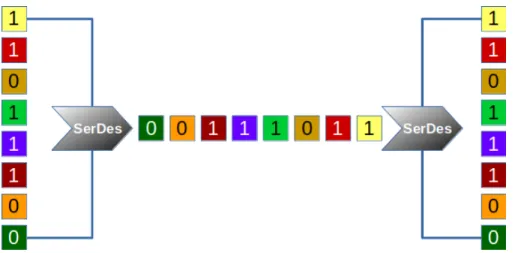
On the other hand, active components are designed in such a way that its routing character-istics may change during runtime, by adding an electrical control system to it. One example of the behaviour of active devices might be given by using the same MR as before, but now assuming it as an active component. Instead of a constant coupling in the same wavelength, it is possible to change the effective index by applying a given current on the MR, thus selecting another wavelength. As expected, active components are more area and power demanding, as they have a more complex structure and make usage of power to change their behaviours. Other components are also usually present when using OINs: signal converters, fast transcei-vers and Serializer(s)/Deserializer(s) (SERDES). Signal converters are used, as the name suggests, to convert signals between domains. The Intellectual Property (IP3) blocks, which generate network traffic are usually digital. So, digital data must be converted to optical signals to be inserted in the network and in the same way, the optical network output has to be converted to digital signal to be processed by IPs. Still, when using OINs, the designer can define whether the network will send messages bit-by-bit or word-by-word. In cases where the sending is performed bit-by-bit, it is necessary to use a SERDES, a device applied to the serialization and de-serialization of a message. On the sender side, this device receives a word and returns it, bit-by-bit. On the receiver part, the SERDES receives a word, bit-by-bit and returns it as one entire word. Figure 2.9 illustrates an example of a SERDES block. The input message is an 8-bit word array. The figure represents the serialization, where each bit is shown one after the other and lastly the deserialization, where all bits are grouped as an 8-bit word array again. Finally, fast transceivers are used to adjust the data rate injection and reception, as the IP blocks operating frequency might be different than the frequency needed on the network.
3An IP block can be defined as any computational unit: a processor, a memory or a DSP, for example.
Figure 2.9 SERDES block exemplification showing an 8-bit word being serialized and later deserialized.
Figure 2.10 shows an organizational example of a system using an OIN with the aforemen-tioned components. In the figure, the internal structure of the OIN is not detailed, rather highlighting only the connections with the IPs. The figure also illustrates the connections among components.
Figure 2.10 Organizational example of OIN-based system illustrating the data flow, passing by the IP, the SERDES, the transceiver, the signal converter and network switch.
2.2 Control Unit
When talking about OINs, the design of the controller of the system is as important as choos-ing the right topology. Unlike eNoCs, optical networks do not rely on buffers to temporarily store data at every switch. If that were the case, it would be necessary to convert all data to digital signals and then re-convert back to the optical signals, leading to high and undesired costs. Thus, the controller algorithm is usually based on one of the following techniques:
• Time sharing, where time windows are set for each IP to transmit its information. On each time window, a set of IPs is granted to send their data, while the others are stalled until the time window ends;
• Dynamically paths setting, which presents a behaviour similar to the one found in circuit-switching eNoCs. The path is defined at the beginning of the transmission. In this context, the controller should compute all the input requests and choose all paths, either by assigning wavelengths on passive-based networks or by tuning the components of active-based networks, and;
• Wavelength division, uses the parallel communication capabilities of optical devices to transmit separate signals. This technique divides the total available bandwidth into a series of non-overlapping sub-bands, assigning a different wavelength for each trans-mitting IP. Usually this technique is employed for passive networks, but not exclusively.
2.2.1 Time Sharing
There are cases where the topologies are built using components that have exclusive access, i.e., allows a single transmission at a time. When this happens, the control unit must manage the requests and granting in a manner that no request waits forever. Figure 2.11 presents a scenario composed of seven communicating blocks that share a single communication medium and a centralized controller. In this case, it is possible to notice conflicting situations that may occur when more than one communicating block tries to access the shared media at the same time.
To prevent this kind of situation, a common approach is to use a time sharing/division multiplexing (TDM) algorithm [41], which divides the time into several recurrent windows (slots), being one for each IP. The time slots might have the same duration depending on the priority attributed to the IPs. Also, the amount of information transmitted over the media on each slot may either be the same for all the IPs or vary according to their priorities.
Figure 2.11 Resource sharing system example, where one simple bus is shared between dif-ferent communicating IPs. The controller (left box), receives requests and grants access to one IP at a time.
The simplest implementation for this kind of situation is based on the Round-Robin Algo-rithm [42]. It implements a first-in-first-out (FIFO) queue, which stores in each position a single IP ID. For every new time slice, the ID found on the next output of the FIFO has its access granted. This kind of control imposes a fair time overhead on the system, being usually deployed on a single, centralized control unit, being more suitable for a lower design complexity, such as low radix systems.
Figure 2.12 shows an organizational example of using an OIN with a centralized control unit. In the figure both the control and network are integrated as one black box.
2.2.2 Dynamically Paths Setting
Another possibility when controlling OINs concerns a circuit-switching (CS) technique. It is a suitable technique used in dynamic network configurations, where an electrical layer has access to all network nodes and configures those needed for each communication to perform correctly. The main appeal of the circuit switching is its utilization on the 3D stacked integrated-on-chip systems, in which each layer of the chip holds one parcel of the entire architecture [43].
In circuit-switching, each optical network node is directly connected to one electrical net-work node. The latter is then physically placed above/under the optical node, using intra-connections such as Through-Silicon Vias (TSVs) [44, 45] to share information between each other. The IPs are connected to electrical nodes and requests travel along all the electrical path, thus closing their way from the origin until their destination. By the time the path is closed, the message starts to be sent through the optical path.
Figure 2.13 shows an overview of the stacked networks and their connections. In the figure, the network nodes are illustrated as blocks, where each block is a network router. Figure 2.13(a) presents the top system view. Figure 2.13(b) shows a lateral systems view, where it is possible to see the connections between the electrical and optical nodes. Figure 2.13(c) illustrates the optical network layer. Finally, figure 2.13.(d) indicates the electrical layer showing the IPs connected to the routers.
Figure 2.13 System overview using a distributed circuit-switching-based control unit; (a) presents the upper view of the system, where the optical layer is placed above the electrical layer; (b) shows the system view from the side. The layers connections are presented as arrows, and communicating nodes as rectangles; (c) illustrates the optical layer, its switches and connections; (d) presents the electrical layer, its switches, IPs and connections.
interesting for systems where large messages are exploited. This occurs since the high cost to close the path can then be compensated by the gain to transmit the message.
2.2.3 Wavelength Division
The last technique applied to control units for OINs is the Wavelength Division Multiplexing (WDM) [46]. This technique is very similar to the TDM. However, instead of using different time slices, WDM employs different wavelengths. When using WDM, the available bandwidth of the channel is divided into sub-channels. For each sub-channel a given wavelength is attributed [47].
Figure 2.14 depicts an example of the usage of a WDM-based controller interacting with four requesting IPs which requires access to the network simultaneously. For each one of them, the controller attributes one different wavelength (λ). This way, the four IPs can transmit data in parallel.
Figure 2.14 System overview using a centralized wavelength-division-based control unit.
This technique allows wavelengths overlapping to be used for two different scenarios: (i) different IPs requesting access simultaneously, as presented in Figure 2.14, and; (ii) for the cases when only one IP is requesting access and all wavelengths are free. In both cases, the controller might attribute more than one wavelength to the same IP, so its transmission might occur in a parallel stream.
2.3 High-level Modelling Strategies and Description Languages
Large system developers usually struggle to precisely identify all aspects that comprise their design, such as the number of components4 and proper abstraction implementation. In
current digital systems, such as multiprocessor embedded systems, it is possible to find from hundreds to thousands different components working together, communicating with each other and depending on each other’s responses.
Therefore, for a designer to effectively capture and manage all these aspects, higher abstrac-tion levels are mandatory. In this way, a model might be defined as a simplified vision of anything real and, in order to decrease the system design complexity, different models are used. For instance, a computation system can be defined as a set of digital ports, as a series of logical transactions or as a single I/O block.
Diverse challenges arise when modelling current systems. Among those, we highlight model complexity, simulation runtimes and analysis complexity, model abstraction, complex inter-dependencies, and parallel components.
The Unified Modelling Language (UML) [48, 49] is a general-purpose modelling language designed to be used as a standard description modelling language. It relies on visual blocks to describe all system architectural contents: transactions, components, timing, data flow, etc. Most visual high-level modelling tools use the standardized patterns (UML blocks and their connections) adopted in UML.
In the case of the Petri nets [50], directed graphs are used to model distributed systems, and the system is described as a series of places, transitions and directed arcs. Each place represent a component or logic block. All these places are connected by arcs. For the flow in the net, transitions are used, which represent the movement from one place to the other, passing through transitions. The system flow of a Petri net always follows the same behaviour, where one arc moves towards another passing by one transition.
Another model type is the Kahn Network [51], in which sequential processes communicate through FIFOs. Its main characteristic is the synchronization imposed by the FIFOs, which makes this kind of model suitable for distributed, communicating systems.
Besides specific models, different languages are defined for specifications as well. Although their usage is not restricted to one specific functionality, their focus is usually well defined. Architecture Description Languages (ADL) [52] are designed to describe and represent system architectures. ADLs might be used to describe both software and hardware. For software, ADLs cover features such as processes and threads. For hardware description, ADL describes components, such as processors, devices and buses. Also, the connection between the com-ponents is described in ADL. For instance, a processor can be described in ADL as a simple device that receives requests and returns a value.
known as Avionics Architecture Description Language. It is largely used in the modelling of real time embedded systems, to describe either hardware or software components.
Hardware Description Languages (HDL) focus on describing the characteristics of hardware components. It is possible to describe logical ports, components such as processors and memories and even systems. The main appeal of HDLs lies in the fact that they hold a close relation to the physical layer. Still, it is possible to use HDLs in a way that such physi-cal aspects are abstracted and only the behaviour is captured. This makes HDLs powerful description languages to be used when designing systems. By using these languages, at-tributes like time, components concurrent execution and connecting signals can be modelled. The most common languages in this group are VHDL [54] and Verilog [55]. Programming languages are a different group of specification languages, where the focus is on software deployment. Usually, they act as an interface between the hardware and the user. Common examples of this group are C++ [56] and Java [57].
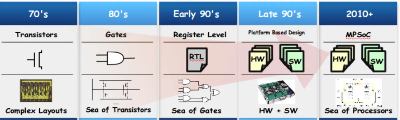
Throughout the years, the modelling abstraction level has been upgraded and the introduc-tion of digital designs has led to the need for reducing design complexity by increasing the system-level view. Figure 2.15 presents the evolution of the abstraction level used on the deployment of digital systems. Starting from the transistor - the fundamental design unit - the abstraction level started to rise. First, a digital system was represented as a set of logical ports, then registers, and finally as hardware and software models. In the figure, four rows are presented: the timeline, the device abstraction, the modelling level and the system overview.
Figure 2.15 Design Abstraction Levels
It is possible to see that the level of modelling method cope with the complexity of the state-of-the-art systems. As new functionalities are added to systems, the modelling strategy has to be updated as well. At first, systems were simpler than nowadays, which made it possible
to describe them one transistor at a time. Later, systems evolved from groups of transistors to big sets of logical ports, which lead to the utilization of Register transfer level (RTL) languages. Nowadays, systems incorporate different elements, as hardware components and software logic. For designers to capture all different aspects involved in the description of such systems, higher-level modelling strategies are adopted. The concepts of high-level modelling, like ADLs and UML are employed for these systems. In the next systems’ generation, not only different elements will be present, but also different technologies, where systems will be heterogeneous. Future systems will be composed of digital hardware, such as processors; magnetic components, as magnetic RAMs; logic models, as software; optical components, such as OINs. This makes mandatory the update of current design methods. The update may be achieved by the definition of new modelling languages, where such aspects can be described. Another possibility is the re-utilization of nowadays modelling languages, by employing them in different contexts. While developing new languages for the description of future systems would make them perfectly suited to the context, the re-utilization is appealing, as it takes advantage of mature approaches.
CHAPTER 3 RELATED WORK
This chapter summarizes the most important related works in the field of OINs modelling and simulation as well as controllers for OIN-based systems. Section 3.1 introduces a set of tools and methods to simulate, model and evaluate optical systems. Their description will be divided into two sub-sections: one presenting a discussion about industrial tools and one focusing on academic tools. Moreover, Section 3.2 presents a discussion of state-of-the-art controlling solutions for OIN-based systems, where recent and relevant publications on the field are discussed and their methods are explained.
3.1 Modelling, Simulation and Evaluation
The design of optical devices is a complex task, requiring different variables to be consid-ered. Optical devices are sensitive to dynamic variations, such as temperature and even a small deviation can change the device behaviour, making it mandatory to capture all those small peculiarities. This way, different approaches and tools were made available by either industrial or academic research. These tools can focus on the entire design flow or specific aspects, such as power loss. In this chapter we will focus on tools considering the design from a system-level perspective.
3.1.1 Industrial Tools
Facilitating the employment of optical devices, several companies provide tools and method-ologies for engineers to use. Those tools usually cover the entire design flow, from the very beginning, when each device is modelled and the integration of developed devices. These kind of tools depends on numerical methods and solvers to compute all variables that compose the system, which are usually complex and processing demanding.
One example of industrial state-of-the-art company is Lumerical Tools [58], which provides an environment for the deployment of optical devices, from the initial level till the integration level. It has four applications that might be run solo or in an integrated way, following a design plan. Designers can start their device from scratch using MODE, adopted to model the device and make initial verification, like group index. The second application in the design flow is FDTD, which is a 3D Maxwell solver that analyzes the light interactions on different wavelengths scales. Following, Lumerical presents INTERCONNECT, a photonic integrated circuit design environment that enables the design, simulation and analysis of
photonic integrated circuits. INTERCONNECT is able to perform analysis either on the frequency domain or in the time domain. Last of four Lumerical Tools is the DEVICE Tool which is used to integrate photonic and CMOS devices.
VPIPhotonics provides a set of tools for the design of Photonics devices with the difference that most of their tools focus on long-distance communication systems. The provided tool for Photonic Devices design and optimization is the VPIcomponentMaker Photonic Circuits [59], a tool with a focus on photonic integrated circuits (PICs), electric circuits, and optoelectronic devices.
Optiwave [60] is a design suit for the deployment of photonic devices. It offers a great list of applications to ease the project of such systems, making it possible to even integrate their tools with available electrical tools, like Matlab [61]. Optiwave also provides SPICE tools for integration with CMOS devices.
Some other tools might be cited as well, like OptSim [62] and Optilux [63], which also provide support for the development of Optical Devices. These tools present features such as numerical solvers for the analysis of physical aspects of modelled devices.
Aforementioned tools are accurate and provide feedback, relying on precise models to repre-sent the system. By using them, designers can entrust that obtained results are very close to the fabricated devices. However, as implemented models depend on complicated equations and analytical models, their computation time is large, jeopardizing their effectiveness for large systems, limiting their usage to small systems. Although it is important to acknowledge the high complexity to attain the level of accuracy of such tools, the fact that they do not contemplate the entire system design puts at risk the time-to-market.
3.1.2 Academic Tools
In order to support system-level design, initial tools were made available by academy. These tools are meant for academic purposes and are firstly focused on proving new methods and theories. Also, such tools are usually designed for one specific purpose, like analyzing crosstalk [64, 65], thus not allowing an entire system deployment. In this way, with very specific purposes are not covered in this review.
Among system-level tools, it is possible to split them in two groups: extensions on already existing simulations tools and the ones implemented from scratch.
PhoenixSim [66] is an example of a simulator extension. It is built based on the
OMNeT++ [67] framework, a well-known network simulation platform that allows users to extend its functionalities. PhoenixSim may be used for designing and analyzing the
per-formance of photonic interconnection networks, generating reports for propagation delay, insertion loss, extinction ratio, spectral resonant profiles, area occupation, and energy dissi-pation.
GRAPHITE [68] is a distributed simulator for multi-core systems. The focus of this tool is to reduce the simulation time, by splitting the computation overhead among different CPUs in a network, thus giving a fast feedback on different validation scenarios.
An accurate and promising tool was introduced by [69], named DSENT. This tool presents models to simultaneously simulate electrical and optical devices and providing different re-ports, such as area usage and power consumption. The developed models are precise and rely on information extracted from physical libraries for different technologies, such as 45 nm, 32 nm, 22 nm, 14 nm and 11 nm.
Some other tools used as bases for the design of system simulators are Booksim [70] and NoCSim [71], both projected to validate eNoCs but, thanks to similarity between approaches, can be extended to validate ONoCs as well.
The main issue with these tools is that they are still deeply attached to a component view, making their usage difficult for dynamic scenarios, with applications running and real-time changes occurring. Also, most tools are designed to exploit one specific design constraint, such as power loss, thus leaving the support for all other aspects unattended. While their focus was on solving one specific metric, it is important to highlight that all the design context must be covered.
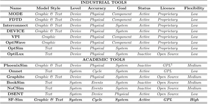
In this work, the Straight-forward Simulator (SF-Sim) is introduced. The fundamental dif-ference of the aforementioned tools and the SF-Sim lies on the fact that the proposed tool gives engineers an accurate feedback, maintaining obtained results close to the ones obtained in real systems. At the same time, the SF-Sim enables the design flexibility of a system-level perspective. Designers have the opportunity to create systems from scratch by using pre-defined components in a library or by adding new ones using the developed methodology. Table 3.1 presents the comparison between previous tools and the one proposed in our project, emphasizing the following points:
• Model Style: description model provided by the tool. Might be textual, graphical, etc;
• Level: abstraction level of the tool;
• Accuracy: the given accuracy, such as: cycle, physical, events, etc. For instance, if the tools run at a clock-base, it is defined as cycle accurate and if it runs as series of
events, such as application transactions, it is defined as events;
• Goal: focus of the tool. If a tool lets users design an entire system, but is meant for devices only, the design goal will be defined as Device;
• Status: if the tool development and user support is either active or inactive; • Licence: the type of licence required for users to have access to the tool, and;
• Flexibility: the flexibility to describe models using the tool, from a system-level per-spective. In other words, the degree of easiness to describe a system, using available modelling strategy. This comparison is performed based on the functionalities pre-sented by the tools as well as in hands-on experience. For instance, some tools present a deep support to evaluate preloaded optical networks. Still, if needed, the designer cannot add new topologies or systems, thus diminishing the flexibility of the tool.
Table 3.1 Tools Comparison
INDUSTRIAL TOOLS
Name Model Style Level Accuracy Goal Status Licence Flexibility
MODE Graphic & Text Device Physical Component Active Proprietary Low
FDTD Graphic & Text Device Physical Component Active Proprietary Low
Interconnect Graphic & Text Device Physical System Active Proprietary Low
DEVICE Graphic & Text Device Physical System Active Proprietary Low
VPI Graphic Device Physical Component Active Proprietary Low
OptiWave Graphic Device Physical Component Active Proprietary Low
OptSim Text Device Physical System Active Proprietary Low
OptiLux Text Device Physical System Inactive Open Source Low
ACADEMIC TOOLS
PhoenixSim Graphic & Text Device Physical System Inactive GPL1 Medium
Omnet Text System Cycle System Active GPL Low
Graphite Graphic & Text Device Physical System Active Open Source Medium
BookSim Text System Events System Inactive Open Source Medium
NoCSim Text System Events System Inactive Open Source Medium
DSENT Text System Device Physical Active Open Source Low
SF-Sim Graphic & Text System Cycle System Active GPL High
1 - General Public License (GPL).
3.2 Controlling Schemes
Most state-of-the-art works opt for designing a network controller that is suited for a specific topology or type of architecture, thus optimizing at most its performance. This way, most of proposed controllers are presented along a specific topology or router structure.
In [72], the authors present the design of a 5x5 MR-based router, which uses a mixed active-passive design approach. It is designed to active-passively route the optical signal travelling in one direction and actively route the optical signal making a turn. The authors claim that this router is designed in such a way that it is scalable to be used as a basic block for large networks. The control unit used for the proposed router is a circuit-switched-based one, where XY algorithm is applied on the electrical layer and closes the paths for the optical layer. The main drawback of this approach lies in the fact that circuit-switching techniques are time demanding and as the network’s size grows their response time might get prohibitive. In [73], a new architecture for photonic networks-on-chip is presented, along with its control-ling scheme. The overall power consumption of the system is claimed to be reduced by using a dynamic resources provisioning. Each electrical router, on the electrical layer, is connected to a processor with private L1/L2 caches, and routers and processors are located above the corresponding optical switches. The electrical router and the optical switch communicate through TSVs1 and optical/electrical signal converters on the control die. Each electrical
router contains four I/O interfaces. The controlling layer works along with the Network In-terface (NI). The NI role is to activate/deactivate laser sources in order to save power, after the controller triggers the beginning/end of transmissions. Once again, the technique used to define either if an IP will have access to the network or not is by using circuit-switching. Also, to guarantee message delivery, a given time is used before turning the laser source off, where the time is defined according to the number of hops the message will pass by and is dynamically calculated by the controller. The latency of such method was calculated to be around 3.5ns in an 8×8 network where resonators and peripherals run at 5GHz. The ar-chitecture was validated on a simulator built over Simics/GEMS framework [74]. The main comment that might be addressed for the solution proposed by the authors is that the usage of circuit-switching for path allocation is very expensive in resource allocation and, even for a fairly small network size (eight IP nodes), the control latency is high (for a 5GHz frequency operation, the period is equal 0.2 ns, meaning that it takes around 17 clock cycles for every request to be computed).
The work presented in [75] brings the design of an ONoC which is an extension of previous works, like the λ-Router [76], but reducing resource utilization. The technique used by the authors to reduce the resources utilization is similar to clustering, where the switches are grouped in small blocks, thus dividing the network in small versions of itself. The number of used resources in which a message may pass is reduced because as it goes in one direction all nodes in previous directions will never be visited. The control unit is based on wavelength
routing, where each I/O is assigned to one specific wavelength and might communicate at any time, without arbitration. Although this kind of structure solves any kind of contention, the overhead imposed by this solution is high, as for every I/O port, ’n’ buffers must be used, being n = number of IPs. Still, each I/O requires a specific wavelength, which is difficult to implement from an optical perspective. This is due to physical limitations, which curb the number of possible wavelengths to be used. This way, in a system with a big number of I/Os, not enough wavelengths would be available.
Authors of [47] introduce a routing technique based on wavelength selection integrated with spatial routing. The main contribution authors claim is that classic circuit-switching tech-niques are too time and resources demanding and based on that they present an extension of such methods. Their technique is based on the unused spectrum that exists between the resonances of a broadband ring switch by interleaving additional wavelength channels in the unused spectral space. That way, instead of having simple wavelength selection a wavelength division multiplexing (WDM) selection is used, where each group is an isolate case. The Circuit-switching technique is used along WDM and each router is composed of a junction of a receiver bank and a modulator bank. The design was tested with the electrical layer running at a frequency of 2.5GHz. The results for timing improvement of the introduced technique shows a reduced latency. Still, even for small messages passing (100-kbit messages, for instance), using a 100Gbps (gigabits per second) transmission rate, the checked latency reported is around 100 ns, which is high, taking into account the fact that this controller is fully tailored for the architecture it is designed for. Consequently, it is not possible to apply it to different network topologies.
An electrical-optical mixed approach is brought by [77], where a butterfly-based topology is introduced and each node is composed of an optical switch and an electrical switch. Optical switches are composed of MRs and are in charge of transmitting data on a circuit-switching fashioned way, while electrical switches are in charge of closing the path by using package-switching techniques. The main contribution of this solution is the fact that, after a set of trials, if the control unit is not able to close the optical path, the message will be transmitted using the electrical layer directly. As for the other cases where circuit-switching is used, the tuning time necessary to close the optical path is the main issue.
An asynchronous and variable-length packet switching is presented in [78]. This technique uses a two layered approach to dynamically set the message path over the network. Every IP is attributed to one exclusive label, which corresponds with each output fiber, for sending out switch fabric reconfiguration. While the message travels over the optical path, when it comes across a new network node, the message gets delayed while its label is computed by