HAL Id: tel-00976618
https://tel.archives-ouvertes.fr/tel-00976618
Submitted on 29 Apr 2014
HAL is a multi-disciplinary open access
archive for the deposit and dissemination of sci-entific research documents, whether they are pub-lished or not. The documents may come from teaching and research institutions in France or abroad, or from public or private research centers.
L’archive ouverte pluridisciplinaire HAL, est destinée au dépôt et à la diffusion de documents scientifiques de niveau recherche, publiés ou non, émanant des établissements d’enseignement et de recherche français ou étrangers, des laboratoires publics ou privés.
Non-collinear magnetoeletronics in single wall carbon
nanotubes
Alina Dora Crisan
To cite this version:
Alina Dora Crisan. Non-collinear magnetoeletronics in single wall carbon nanotubes. Other [cond-mat.other]. Université Paris Sud - Paris XI, 2013. English. �NNT : 2013PA112327�. �tel-00976618�
UNIVERSIT´
E PARIS-SUD
`
Ecole Doctorale:
107
Laboratoire de Physique des Solides, Paris-Sud
Laboratoire Pierre Aigrain, ENS Paris
TH`
ESE DE DOCTORAT
Soutenue le
17.12.2013
Pr´
esent´
ee par:
Alina Dora CRISAN
Non-collinear
Magnetoeletronics in
Single Wall Carbon Nanotubes
Co-directeur de th`
ese:
Dr. T akis Kontos
Co-directeur de th`
ese:
Dr. Andr´e Thiaville
Composition du jury:
To my family. For the unequivocal support they gave me, no matter what craziness i chose to do.
To Alex. With you by my side, i am ready for a second one.
Acnowledgements
It would not have been possible to complete this doctoral work without the help and support of the kind people around me, to only some of whom it is possible to give particular mention here. The special conditions of this thesis made of the past three and a half years both challenging and enriching ones.
First of all, i would like to thank my two supervisors, Andr Thiaville and Takis Kontos whom, in my perception of things, acted like the two sides of a coin but ex-actly because of this contrast, they made a very good team. Their knowledge, patience and ambition has been an invaluable help during these three and a half years. I wish i had at the beginning of this journey the wisdom of today, to better use all their gifts.
I am most grateful, more than i could express here, to the two persons that helped me enormously with the sample fabrication proceeses: Raphael Weil and Michael Ros-ticher. They, both, have been truly patient and understanding with me. All the results i had during this thesis are due in great part to them. Also, i would like to acknowledge the support i received from the two post-docs i directly worked with: Keisuke Yamada and Shubadeep Datta, who made much easier my permanent "ballet" between two labs and two different research subjects. The same feeling i have for Jean-Yves Chauleau and Cheryl Feuillet-Palma who first introduced me to the subjects i developed in this manuscript.
I must say nanometric scale devices are though to work with. For this reason, i cannot forget the help received from Mathieu Delbecq and Jeremie Viennot with the sample preparation part. Even more, knowing, i am not the easiest person to work with. Also, i have greatly benefited from the generous support of Luc Fruchter and Frédéric Bouquet during my electrical measurements done in Orsay. They, both, en-tered this project in a moment i was loosing hope on one part of this work.
Audrey Cottet, thank you for all the theoretical work you have done, it helped so much in the understanding of the experimental results, giving that "edge" that all ex-perimental work needs. And because i mentioned exex-perimental results, here i need to mention and express my gratitude also to Olivier Andrieu, who saved the day, in more
Maybe the best part of my thesis represented the oportunity to meet many interest-ing people. The back and forth between two labs that was needed in the last few years gave me the oportunity to interact with twice as many persons than other students do. I would like, here, to express my apreciation to all the members of both teams i worked with for their guidance and all the pleasant moments spent together. Gwendal Fewe, Bernard Plaçais and Jean-Marc Berroir, thank you very much for your warm encouragements, given in key moments of this thesis. Alexandra Mougin, Jacques Miltat, Stanislas Rohart, Jean-Pierre Jamet, Vincent Jeudy, Grgory Malinowski and Jacques Ferr i am grateful for the helping hand given with various experiments i had to perform and for the efforts to integrate me in the group. Of great help was the excelent colaboration with Charys Quai and Sylvie Gautier for the metalisations done in Orsay.
Looking behind, i realise that i was truly fortunate people wise. During this thesis i gained some very good friends wit hwhom i shared many pleasant moments. Thank u, Andreas Betz (and lovely Clara) for your tonic company and continuous moral support, Erwan Bocquillon, Jon Gorchon, Jacob Torejon, Quentin Wilmart, Francois Permen-tier, Vincent Freulon and many others for the beautiful memories you have given me. A special, grateful, wink to Clementine Carbillet, your presence and the discussions we had during our usual runs really made a difference in tough moments.
And last but not least, i want to include on this list also to the people outside the labs that believed in me and encouraged me during this thesis. Here i need to mention my family who encouraged me from afar and my friends that sometimes traveled long distances to be next to me or that shared many hours and cups of tea with me. I will open this list with Alex, my best friend and my flatmate during all this time and then i will continue with Ieva, Lars, Cristina and Adrian, Anxi, Becky and Andreas, Jeremy, Riad, Dita, Alina, Ioana, Szonja, Olimpia, Alan, Catalin, Ibtissem, Ramona ... and i would better stop here even if i could go on like this for another half a page.
Contents
1 Introduction 6
1.1 Main results . . . 8
1.1.1 PdNi anisotropy . . . 8
1.1.2 Non-collinear magneto-electronics/Spin dependent transport in quantum dots . . . 10
1.1.3 Coulomb blockade transport regime . . . 11
1.1.4 Fabry-Perot transport regime . . . 14
2 Non-collinear magneto-electronics/Spin dependent transport in quan-tum dots 16 2.1 Spin transfer torque . . . 16
2.1.1 The evolution of magneto-electronics . . . 16
2.1.2 The spin field effect transistor . . . 21
2.1.3 Transport characteristics in nanotubes/nanoconductors . . . 23
2.1.4 Electron tunneling . . . 24
2.1.5 Julliere’s model . . . 26
2.1.6 Magnetic tunnel junctions (MTJ) . . . 28
2.2 Transport regimes . . . 34
2.2.1 Quantum spin valves in weak-coupling regime . . . 37
2.2.2 Magneto-Coulomb effect . . . 39
2.3 Recent experimental work on spin polarized transport . . . 43
2.3.1 Effective fields . . . 47
3 Experimental setup 52 3.1 Sample preparation . . . 52
3.1.1 The substrate . . . 53
3.1.2 The lithographic process . . . 54
3.1.3 The resist . . . 54
3.1.4 The electronic lithography . . . 55
3.1.5 Development . . . 56
3.1.6 Thin film deposition . . . 56
3.1.7 CNT growth . . . 58
3.1.8 PdNi Hall crosses . . . 61
3.1.9 Observations on the sample fabrication process . . . 63
4 Magnetic anisotropy in PdNi nanostripes 68
4.1 General considerations on PdNi anisotropy . . . 68
4.1.1 General considerations on anisotropy . . . 68
4.1.2 Particularity of the PdNi nanostripes anisotropy . . . 70
4.1.3 Normal Hall effect and the extraordinary Hall Effect . . . 73
4.2 Experimental results . . . 75
4.2.1 Role of chemical composition . . . 78
4.2.2 Capping layer effect . . . 81
4.2.3 Thickness effects on PdNi . . . 82
4.2.4 Nanometric samples . . . 84
4.3 Conclusion . . . 85
5 Non-collinear magneto-electronics in nanoscale conditions 86 5.1 Coulomb blockade regime . . . 86
5.1.1 Spin transport in the linear regime . . . 90
5.1.2 Out of equilibrium spin-signal . . . 92
5.1.3 Conclusion . . . 98
5.2 Fabry-Perot transport regime . . . 99
5.2.1 Spin transport in the linear regime . . . 100
5.2.2 Spin transport in non-linear regime . . . 100
5.2.3 Conclusion . . . 101
List of Figures
1.1 Schematic view of a CNT based quantum dot; SEM image of a typical sample. . . 7 1.2 Image of a typical PdNi, Hall cross, taken with an optical microscope. . 8 1.3 Color scale differential conductance spectroscopy of a device displaying
Coulomb blockade transport regime. . . 11 1.4 Gate response of magneto-resistance in coulomb blockade regime. . . . 12 1.5 Spin signal as a function of the magnetic field, B, and the source-drain
VSD. . . 13
1.6 Heuristic illustration of the phenomenological behavior of the QD-based device. . . 14 1.7 Color scale differential conductance spectroscopy and magnetoresistance
curve in linear regime for a Fabry-Perot transport regime. . . 15 2.1 The structure of the density of states of the conduction band in a
fer-romagnet and the state density of the free electrons in a non-magnetic material . . . 17 2.2 Heuristic picture of spin and charge transport into a
ferromagnetic/non-magnetic system. . . 18 2.3 Heuristic picture of spin charge transport and spin current detection in
a ferromagnetic/non-magnetic/ferromagnetic system. . . 19 2.4 Illustration of the magnetization torque exerted by a spin current at a
non-magnetic/ferromagnetic metal interface. . . 20 2.5 Illustration of the direction of the spin torque for both current polarities
in a typical metallic spin valve structure. . . 20 2.6 Illustration of the Datta - Das SFET . . . 22 2.7 Illustration of a carbon nanotube based device based on a FET’s geometry. 24 2.8 Illustration of a rectangular potential barrier of height V and thickness a. 25 2.9 Electrical resistance in a F/I/F’ type of junction. . . 28 2.10 Illustration of the spin torque for both current polarities in a typical
metallic spin valve structure.TMR signal in a MTJ in presence of a sweeping external field. . . 29 2.11 Histeretic curves as a function of an exterior magnetic field obtained by
Suzuki et al in a JTM. . . 30 2.12 SEM image of a dispositive based on CNT connected to collinear PdNi
electrodes working in a Fabry-Perot regime. Differential conduction measurements and variation in conductance records. . . 32
2.14 Heuristic view of a quantum dot connected through tunneling barriers
to the metallic leads. . . 35
2.15 Differential conductance spectroscopy showing different types of trans-port regimes. . . 37
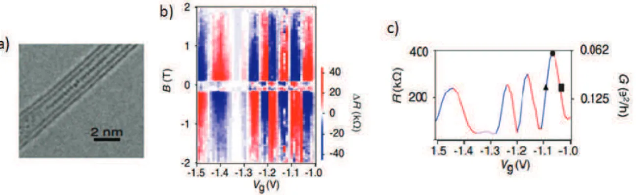
2.16 High resolution TEM image of a portion of a double-wall CNT filled with elongated FeO particles and hysteretic behavior as a function of gate voltage, VG. . . 41
2.17 SEM image of a portion of the CNT filled with FeO particles and the equivalent electrical circuit of the resulted device. Hysteresis plot and resistance of the device as afunction of gate voltage. . . 42
2.18 Experimental results obtained by Sahoo et al on a MWNT based device connected to PdNi leads. . . 44
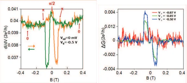
2.19 Spin-dependent tunneling effect in QD-like system connected with fer-romagnetic leads. On resonance and off resonance cases. . . 45
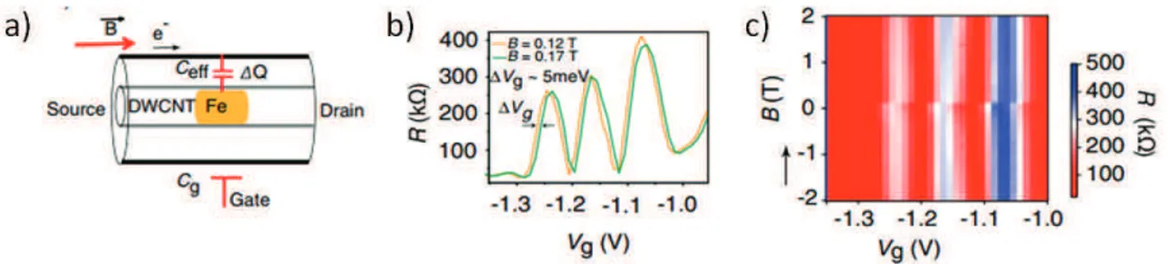
2.20 Grey scale of the nonlinear conductance of the nanotube as a function of the source-drain voltage and the gate voltage. Conductance G and TMR signal, both experimenta and theoretical obtained by Sahoo et al 46 2.21 Ni break junction capacitively connected to a Al gate voltage and to Au contacts experiments done by Pasupathy et al. . . 48
2.22 Ni break junction capacitively connected to a Al gate voltage and to Au contacts experiments done by Pasupathy et al. Kondo regime. . . 49
2.23 Illustration of a CNT-based dispositive. Illustration of the Kondo regime. 50 3.1 Typical SEM image of a CNT based device. . . 53
3.2 Illustration of a typical nanofabrication process. . . 56
3.3 Schematic overview of the sample preparation process. . . 59
3.4 Methane based CVD oven used in the nanotube growth process. . . 60
3.5 Overview of the sample preparation process for the PdNi Hall crosses. . 62
3.6 Typical SEM images of different areas of a substrate displaying different CNTs densities. . . 63
3.7 Electrical diagram of the conduction measurements. . . 64
3.8 Typical images acquired by MFM technique . . . 65
3.9 Typical Hall cross sample; image acquired under an optical microscope. 67 4.1 Phase diagram for P dxN i100−x. . . 70
4.2 Selection of MFM images on different P d30N i70 nanostructures. . . 71
4.3 XMCD-PEEM images taken on P d20N i80 stripes. . . 72
4.4 Illustration of the skew scattering mechanism . . . 74
4.5 Illustration of the side jump mechanism . . . 74
4.6 Illustration of the intrinsic deflection phenomena. . . 75
4.7 Typical Hall cross sample; picture acquired under an optical microscope. 76 4.8 EHE measurements on samples with different PdNi chemical composition. 78 4.9 Capping effect on P d90N i10 Hall crosses. . . 80
4.10 Thickness effect on P d90N i10 Hall crosses. . . 83
4.11 EHE measurements on P d90N i10 samples of multiple seizes. . . 84
5.1 Schema of a quantum dot connected to two non-collinear leads. SEM image of a typical sample in false colors. . . 87
5.2 MFM image performed on a control sample at room temperature. . . . 88 5.3 Color scale differential conductance spectroscopy of a device displaying
Coulomb blockade transport regime. . . 89 5.4 Gate response of magneto-resistance in coulomb blockade regime. . . . 90 5.5 Gate voltage response of the spin signal in color scale as a function of
external magnetic field and gate voltage in Coulomb blockade. TMR modulations with gate voltage. . . 91 5.6 magnetoresistance curves in out of equilibrium conditions in Coulomb
blockade transport regime. . . 92 5.7 Magnetoresistance curve for different values of source-drain voltages in
Coulomb blockade regime. . . 93 5.8 TMR signal and differential conductances as a function of the
source-drain bias VSD for different gate voltages in magneto-Coulomb blockade. 94
5.9 Experimental and theoretical linear conductance curves. . . 95 5.10 Color scale plot of the spin signal as a function the external magnetic
field, B, and the source-drain bias, Vsd. Experimental and theoretical
curves in out of equilibrium Coulomb blockade regime. . . 96 5.11 Schematic picture of the precession place inside the CNT. Effective
in-verse g-factor 1/gef f and linear conductance as a function of gate voltage. 98
5.12 Color scale differential conductance spectroscopy of the device over a wide range of source-drain bias, VSD, and gate voltage, Vg in
Fabry-Perot regime. . . 99 5.13 gate voltage response of the spin signal in color scale as a function of the
external magnetic field, B, and gate voltage Vg in Fabry-Perot physics. 100
5.14 Wide gate voltage response of the spin signal in color scale as a function of the B-field and VSD. Magnetization reversal before the external field
Chapter 1
Introduction
Electronics represents a corner stone for our modern technology. With the recent de-velopment of nanotechnology, people eventually became able to access the adequate length scale to closely investigate the spins and the wide interest and large prospects of using the electrons spin degree of freedom in new generation electronic devices have lead to a vibrant field dubbed spintronics.
In this work, we present experiments in the field of spintronics that combine two very promising materials: single wall carbon nanotubes (SWCNTs) and palladium nickel (PdNi), a tunable ferromagnet, with the purpose to manipulate the electronic spin both in the classical and in the quantum regime. Carbon nanotubes (CNTs) are carbon cylinders of a few nanometers in diameter and up to several millimeters in length. They were discovered by Sumio Iijima in 1991 [1] and they have attracted a lot of interest because of their exceptional electronic and mechanical properties. CNTs have been applied as FETs in logic circuits, and have been also proposed for other elec-tronics applications. More recently, also spin injection and transport in CNTs came under intense scrutiny. The combination of high charge mobility, negligible spin-orbit coupling and weak hyperfine interaction holds the promise of very long spin relaxation times.
P dxN i100−x (where x represents the atomic concentration, in percent) alloy also
at-tracted considerable attention as ferromagnetic electrodes in carbon based spin valves. Its excellent contact properties on carbon nanotubes (CNT), lead to low resistance contacts (transparent) [2], while its ferromagnetic behavior provides the means for spin injection. Surprisingly in the case of CNTs a tunneling barrier between the PdNi and the CNT itself seems not to be an indispensable ingredient for spin injection. In fact the anisotropy of the alloy plays an important role since the successful demonstra-tion of spin injecdemonstra-tion is based on the observademonstra-tion of a giant magnetoresistance (GMR) effect, determined by the relative orientation between the magnetization of the ferro-magnetic electrodes. In carbon-based spin-valve devices the planar arrangement of the system complicates the realization of non-collinear magnetizations, and the ability to control the magnetization direction with respect to the plane of the electrode which is an essential factor in the evolution of the system. For this, a good knowledge of the magnetic properties of such ferromagnetic alloys when lithographically patterned into
narrow electrodes.
Manipulating spin or magnetization requires to apply a torque via a real or an effective magnetic field. Not so long ago it was shown that spin polarized current is another possibility to achieve the same results thanks to the spin transfer torque phe-nomenon [7]. So far, the spin transfer torque has been intensely studied in systems (nanopillars [11], magnetic stripes [45] etc) exhibiting a classical, essentially diffusive, transport mechanism. In this context, the question to ask is: what happens when these classical conductors are replaced by quantum ones such as nanowires or quantum dots. The immediate interest in such systems, beside the fundamental phenomenology involved is a new generation of electronic devices where the spin transfer torque dom-inates over heating and/or Oersted field effects.
Figure 1.1: (a) Schematic view of a CNT based quantum dot: two metallic leads (source and drain) are evaporated on the CNT; the nanotube is capacitively connected to a gate voltage while a source-drain tension is used to vary the chemical potential of the electrodes; (b) SEM image of a typical sample in false colors. The red arrows indicate the direction of the magnetizations. A back gate electrode (not visible) is used to tune the energy levels of the device. As shown by the orange arrow, the external B-field is applied along one of the easy axis of the two PdNi strips. A bias voltage (not visible) is used to tune the electrochemical potentials of the electrodes.
The control which is generally offered when scaling down to nanometric dimensions allows one to achieve new functionalities with high potential, as it is the case of the spin field effect transistors [35], [38]. So far, results of such a high potential have been demonstrated only for collinear geometry-based systems, where spin transport can be described using a single quantization axis. Still, magnetoelectronics devices exploiting actively the electronic spin, meaning a total control over classical or quantum spin rotations have not been achieved so far.
Here we implement a quantum dot connected to two non-collinear ferromagnetic leads forming an angle of θ = π/2, schematically presented in fig. 1.1, (a). The device we propose acts like a spin-valve device. A finite tunneling magnetoresistance effect is to be expected. in fig. 1.1, (b) one can see a SEM image of a typical sample in false colors. The red arrows indicate the direction of the magnetization of the two leads. A back gate electrode (which is not emphasized in the image, see fig. 1.1, (a)) is used to tune the energy levels of the device. As shown by the orange arrow, the external magnetic field, B, is applied along the easy axis of one of the PdNi stripes.
1.1
Main results
1.1.1
PdNi anisotropy
For a better understanding of the magnetic switchings taking place in such a device and also for optimizing its electronic properties, a detailed understanding of the mag-netic characteristics of P dxN i100−x, alloy becomes crucial. During this work we studied
PdNi alloy nanostripes by means of extraordinary Hall effect measurements on litho-graphically patterned crosses (see fig. 1.2) by varying the chemical composition of the alloy, its thickness and the capping films used to impede oxidation.
Figure 1.2: Optical image of a typical Hall cross; the PdNi crosses are connected to Au pads further contacted using a microbonding machine to the sample holder; the principle of a 4-points electrical measurement is exposed in the image: we measure the voltage difference V while applying an electrical current between the I+ and I−
terminals.
The results presented here were measured on samples having 40 µm in width and a length of 100 µm. We investigated also nanometric sized samples with 300 nm in width and 2 µm in length. The thickness of PdNi varied between 5 and 15 nm. Capping layers of aluminium, palladium and samples without capping were probed. All samples
were fabricated on a Si substrate and structured via electron beam lithography. The deposition of the thin films was done using evaporation techniques. Gold (Au) leads are attached to the PdNi crosses as contact pads for electrical measurements; small Au crosses are used to align the patterns during the various steps of lithography. The study focused on P d20N i80 and P d90N i10.
A first question we wanted to anwser to regards the influence that the proportion of Pd in PdNi alloy has on the anisotropy of ones’ samples. For that, both, P d90N i10and
P d20N i80 were investigated. Measurements performed on P d20N i80 for temperatures
between 10 K and 140 K in a field sweeping between −9 T and 9 T show a saturation field between 100 and 200 mT that increases with the increase of the temperature and a lack of remanent magnetization. This testifies for the in-plane magnetization alignment of the sample, even at the lowest temperatures.
The hysteretic curves for P d90N i10, in the same interval of temperatures, show an
evolution from in-plane to out-of-plane magnetization at around 60 K. An increase in the coercive field with the decrease of temperature is emphasized.
An important aspect when considering the transition from P d20N i80to P d90N i10is
lower magnetization of the later alloy (average atomic moment µ = 0.6 B for P d20N i80
while µ = 0.25 B for P d90N i10 as Fischer et al reported [43]), thus a smaller
de-magnetization energy for the P d90N i10. On the other hand, magnetostriction initially
increases with the increase of the Pd percentage in the compound. So, when analyzing P d90N i10we have a smaller demagnetization while more anisotropy in the system thus
a bigger chance to observe an out-of-plane magnetization.
For P d20N i80, this experiment is a first at low temperature and results show that
the magnetization remains in plane even at T = 10 K This translates into a small stray magnetic field exerted by the material which is very helpful in constructing small size spin valve devices with ferromagnetic leads. Indeed, the result is very helpful for the second part of this work, the one concentrated on quantum spin valve effect since an in plane magnetization translates into a small stray magnetic field exerted by the electrodes.
Also a comparison between the Curie temperature of the two alloys: about 120 K for P d90N i10 while for P d20N i80 this is well above room temperature (reported at
600 K by Ferrando et al [40]) offer an obvious facility in the case of P d20N i80 to use
further room temperature techniques for a more thorough investigation. Following these results, in our CNT based spin devices, we used a Ni-rich alloy for the electrodes connecting the CNT, due to the in-plane orientation of the magnetization that
pro-Extraordinary Hall measurements confirm previous experiments [3], [4] that showed a preferential direction of high aspect ratio PdNi contact strips, with a magnetically easy axis transverse to the strip orientation. Furthermore, we provide experimental proof for the model proposed by Chauleau et al who interpreted this magnetically easy axis, transversal to the strip orientation as a consequence of the stress/strain relaxion at the strip edges. While a perpendicular component magnetization effect was also recorded for the core of the stripe, according to Chauleau et al the edges remain trans-verse.
Further measurements show that geometry, thickness and the choice of capping layer used to protect the PdNi against oxidation, are all key parameters when choos-ing the right characteristics for a spin-based device. Measurements done on nanometric sized Hall crosses show a out-of-plane component of the magnetization at small tem-peratures (below 40 K), but less than in the case of the micrometric samples. This is due to due to the stress relaxation at the edges that becomes important, in relative terms, in such small devices.
1.1.2
Non-collinear magneto-electronics/Spin dependent
trans-port in quantum dots
An important factor in quantum dots physics, due to the spatial confinement of elec-trons, is the (Coulomb) electron-electron interaction. The tunneling of electrons from the ferromagnetic electrodes to the island is strongly influenced by the Coulomb charg-ing energy of the QD. Tunnelcharg-ing of an electron into such an island increases the elec-trostatic energy of the island by the charging energy EC = e2/2C, where e represents
the electronic charge and C is the total capacitance of the QD.
When speaking about electron tunneling we need to consider the transparency of the contacts between the CNT and metallic leads. In samples with low contact transparency, a pronounced Coulomb blockade is observed, where single-electron con-ductance peaks are separated by broad valleys of vanishing concon-ductance. To observe Coulomb blockade regime, thus discrete charges inside the QD, one needs that the transmission events between the leads and the island are much smaller than one.
In the case of a more transparent contact between the island and the leads, we can speak about a Fabry-Perot transport regime which is the electronic analog to the Fabry-Perot interferometer. In this regime, the electronic interactions can be neglected.
fer-romagnetic electrodes, of nominal composition P d30N i70, 45 nm thick, covered with
5 nm of Pd. The conductance measurements are done using a standard lock-in detec-tion technique. Each magnetoresistance plot was obtained by averaging 4 times single curves, all displaying a hysteresis switching. The external magnetic field is applied along the direction of one of the electrodes and thus perpendicular to the second one to ensure the maximum effect differences while swept between ±0.4 T .
1.1.3
Coulomb blockade transport regime
Transport measurements revealed a Coulomb blockade transport regime, confirmed by a color scale differential conductance map of the device (see fig 1.3) as a function of the source-drain bias VSD and the gate voltage Vg for the transport spectroscopy over a
wide range of voltages. The color scale plot displays specific Coulomb diamonds char-acteristic to the spectroscopy of a quantum dot. The mean level spacing variate with the gate region: from smaller in the gate region displayed (< 1 meV ), to substantially larger (about 3 meV ) for more positive values of the gate.
Figure 1.3: Color scale differential conductance spectroscopy of the device as a function of gate voltage, Vg (over a wide range), and source-drain bias, VSD. Characteristic
The sample was further tested in both linear regime (in the absence of a source-drain voltage) and non-linear one. In linear regime, results show a typical TMR signal when placed under the sweeping field, behavior specific for a spin-valve device. The hysteretic switchings are symmetric with respect to the 0 external magnetic field and correspond to modifications in the relative magnetization of the electrodes.
Figure 1.4: Gate effect on magneto-resistance (a) Single magnetoresistance curve for Vsd = 0 mV and Vg = −0.5 V . The orange curve corresponds to increasing magnetic
field (Gtrace). The green curve corresponds to decreasing magnetic fields (Gretrace).
(b)Variations of the jumps magnitude (∆G = Gtrace − Gretrace) were observed for
different values of Vg .
Plots of the conductance, dI/dV , as a function of Vg show a clear high conductance
for negative gate voltages. In fig. 1.4, (a), it is displayed a typical hysteretic swich registrated for a gate voltage: Vg = −0.5 V where is indicated also the evolution of the
relative angle between the magnetizations of the two ferromagnetic electrodes. The first switch can be translated as the return of the magnetization in one of the leads leading to the relative degree between the two magnetization of θ = π. The second switching event is attributed to a modification of the angle θ from π to 0. If one defines the amplitude of the hysteresis, ∆G, as the difference in conductance upon in-creasing the external magnetic field, Gtrace, and decreasing the external magnetic field,
Gretrace, then as it can be seen in fig. 1.4, (b), for different gate voltages (Vg = −0.87 V ,
Vg = −0.85 V Vg = −0.5 V ) the jumps magnitude changes.
The TMR signal oscillates with the gate voltage due to the quantum behavior of the nanotube connected to the leads. The oscillations of the TMR stem from quantum interferences phenomena as well as interactions taking place inside the device.
Figure 1.5: (a) Wide range gate voltage variation of the spin signal ∆G = Gtrace − Gretrace in color scale as a function of the magnetic field,B, and
the source-drain VSD. Vg = 0.21 V ; (b) Black line - linear conductance measured
simultaneously with the spin signal, red line - prediction of the proposed model with appropiate parameters.
In the non-linear regime the hysteresis signal (the spin signal ∆G = Gtrace−Gretrace)
measured on a wide source-drain voltage range as a function of the magnetic field, B, for a gate voltage Vg = 0.21 V (displayed in fig. 1.5, (a)) it can be identified a change
of sign as the bias changes from positive to negative values. Also the TMR displays a nearly anti-symmetric behavior around the 0 magnetic field point (see fig. 1.5, (b)). Measurements done for different values of the gate voltage account for the non trivial-ity of this behavior. Comparison of the expermental data with calculations supports the hypothesis of an interplay between spin accumulation phenomena which tends to force the spin inside the dot to follow the symmetry of the current and spin relaxation that acts against it, a precession of the spin inside the QD (see schematics in fig. 1.6) is taking place.
Figure 1.6: Illustration of the phenomenological behavior of the device. A single active energy level carries a single spin which can take in principle any direction since it is controlled by non-collinear electrodes. A concurential behavior between spin accumulation phenomena which tends to force the spin inside the dot to follow the symmetry of the current and spin relaxation that acts against it, determine a precession of the spin inside the QD.
1.1.4
Fabry-Perot transport regime
Colorscale plots of the conductance as a measure of the source-drain and gate voltages confirm the chessboard like pattern specific to the Fabry-Perot physics. The spacing between the centers of two adjacent rhombs gives access to the spacing of the energy levels inside the quantum dot (QD) which is, experimentallly, determined by, L, the length of the nanotube: ∆E = hvF/L. In our case the spacing between rhombs is
5 mV as highlighted in fig. 1.7, (a), using orange dashed lines and it is consistent with the lithographically defined length of the nanotube which is about 600 nm.
Measurements performed in the linear regime were used to characterize the spin transport in the absence of a source-drain voltage. The signal registered has a hys-teretic evolution, with the switchings indicating modifications in the magnetization of the PdNi leads. Measurements done on a large interval of gate voltages show consistent variations in the jumps magnitude up to 4 %.
A striking result obtained here in presented in fig. 1.7, (b). A similar hysteretic curve was obtained in out of equilibrium transport regime for multiple gate voltages values. The hysteretic signal shows magnetization reversal in the electrodes taking place before the external magnetic field applied changes sign. The phenomena was studied both when the field increases and decreases.
Figure 1.7: (a) Color scale differential conductance spectroscopy of the device over a wide range of source-drain bias VSD and gate voltage. Characteristic chessboard
patters - highlighted by the yellow dotted line, specific to Fabry-Perot physics. Experi-mental temperature is 1.8 K. (b) Single magnetoresistance curve for Vg = −1.95 V .
Magnetization reversal before the external field changes sign.
While it is too early for a final conclusion on the nature of this result, this pre-liminary work may suggest a transfer torque that "helps" the external applied field to switch the magnetization inside the two ferromagnetic PdNi leads. This result is even more important since it represents a first in such type of structure. Nevertheless more investigations need to be pursued to present a final picture of the phenomenology involved.
Chapter 2
Non-collinear
magneto-electronics/Spin dependent
transport in quantum dots
2.1
Spin transfer torque
In an era of information and communication, there is a high interest towards new tech-nology related to the interaction with the information. Therefore, research branches bound to generate a better organization, storage, transmission and reading of the in-formation are all in the focus of the scientific community.
Spintronics is the field in which the accent falls on exploiting both the intrinsic spin of the electron and its associated magnetic moment, in addition to the fundamental electronic charge. The discovery of giant-magnetoresistance (GMR) by Fert et al. [5] and Grunberg et al. [6] in 1988 became the monumental moment that spin transport came into mainstream.
2.1.1
The evolution of magneto-electronics
Electrons, as charge carriers, have a property known as spin which is an angular mo-mentum intrinsic to the particle. The quantum mechanical nature of the spin deter-mines that an electron can be described using only two states, with the spin pointing either "up" or "down" (the choice of up and down being arbitrary). An electrical current passing through a macroscopic, non-magnetic conductor is unpolarized due to the fact that spins are randomly oriented.
Things change when ferromagnetic components are incorporated into electronic de-vices. The particularity of the ferromagnetic materials is that the electron’s magnetic dipoles are aligned in the same direction, their individual magnetic momentum added together creating a measurable macroscopic magnetic moment. In materials with a
filled electron shell, the total moment of the electrons is zero because the spins are in up/down pairs. Only atoms with partially filled shells (i.e. unpaired spins) can have a net magnetic moment, so ferromagnetism only occurs in materials with partially filled shells. Ferromagnetism involves an additional phenomenon, though: the dipoles have to align spontaneously, giving rise to a spontaneous magnetization, even when there is no applied field.
Figure 2.1: (a) The structure of the density of states in the conduction band for majority spin (↑) and minority spin (↓) in a ferromagnet; (b) density of states for the free electrons for a non-magnetic material
Using magnetic engineering, the intrinsic bistability of the ferromagnet materials was used to construct device elements with multiple magnetic states. To gain control over both the output/input of such elements, these magnetic states must be converted into something that can be easily manipulated, e. g. voltage or current. Due to spin-based interactions between the ferromagnets and electrons, the orientations of the magnetization for ferromagnetic elements can determine the amount of current flowing through the system. The reverse phenomena in which we can control and vary the orientation of the ferro’s magnetization become also possible.
A good method to do so, is to exploit the spin state of the conduction electrons. In fig. 2.2, one can see how electrical current can be used to detect the magnetic state of a ferromagnetic element (F ) [7]. We contact the ferromagnet with a normal conductor N and the entire system to a current source. We consider the magnetization of the ferromagnet to be uniformly orientated to the +x axis. The magnetic moments of the conduction electrons in the ferromagnet are aligned along the axis of magnetization.
The current crossing the F/N interface will be composed by spin-polarized elec-trons that can diffuse on quite long distances into the non-magnetic material before having their spin orientation randomized. Johnson and Silsbee [8] first reported
dif-the spin orientation. They can be described as spin-polarized conduction electrons. Conventionally, we denote the electrons having their spin oriented along the +x axis as having a spin-up while those pointed towards -x are called spin-down carriers. The conduction electrons of the normal element, N, are not spin-polarized.
Figure 2.2: Heuristic picture of spin and charge transport in a ferromagnetic/non-magnetic, F/N, system.
A second ferromagnet F ′ is used as drain. We create thus a sandwich structure, called a spin valve, in which we place a nonmagnetic material N between two ferro-magnetic ones: F acts as spin injector and F ′ fulfills the role of spin analyzer. We consider that F and F ′ can be controlled separately. If the two ferromagnets have parallel magnetization and orientation, the spin-polarized carriers are driven from F through N and then to F ′ with relative ease. If the magnetization are antiparallel, then the spin current generated through the structure is small, due to the high resistance of the system. A more extensive explanation of this phenomena is given using Julliere’s model in section 2.1.5.
If we consider the magnetization of F as being fixed and we vary only the magne-tization of F ′, then the structure we just depicted, F − N − F ′, represents a model of memory cell in which the output is evaluated through the reading of the electrical resistance of the device given by the alignment of the two magnetizations. More gen-erally, the method presented above represents the way the spin state of an electron can be directly accessed through it’s electrical charge, becoming thus a controlling pa-rameter that can be used to obtain new functionalities for a device. In a similar way, other properties associated to the magnetic state (like magnetostriction) can be used as control parameters.
Figure 2.3: Heuristic picture of spin charge transport and spin current detection in a ferromagnetic/non-magnetic/ferromagnetic, F/N/F ′, system.
An aspect of great interest is that the spin current flows through an interface even at zero applied bias, if the magnetizations of the two ferromagnetic layers are non-collinear; the source of the exchange coupling can be understood as the transfer of angular momentum from this spin current to each magnetic electrode. In this case, the current doesn’t merely respond to the magnetization of the layer but actually al-ters it. When an electron, with misaligned spin, passes from a non-magnetic into a magnetized material, the mismatch gives rise to a small twisting force a torque -between the electron and the magnet.
In fig. 2.4 it can be seen how at a non-magnetic/ferromagnetic interface, by means of conservation of angular momentum, the ferromagnetic material absorbs the trans-verse component (with respect to its own magnetization) of the angular momentum of an incoming electron, which acts on the magnetization of the material as a torque. At the same time, the parallel component of the angular momentum is reflected back into the normal conductor. A large current generated like this can in principle shift the magnetization direction of the material that it is passing through.
Figure 2.4: Illustration of the magnetization torque exerted by a spin current at a non-magnetic/ferromagnetic metal interface. The magnetization of the ferromagnet is normal to an incoming electron that can be written as a linear combination of the "up" and "down" spin states. Assuming that the interface is transparent only to the spin having the same orientation as the magnetization, M , of the ferromagnet, the parallel spin and charge currents are conserved, whereas the transverse spin current is absorbed and acts as a torque on the magnetization.
Some very important papers, launching the study of spin transfer torques appeared in 1996, when Slonczewski [9] and Berger [10], independently, showed that current flowing perpendicular to the plane in a metallic multilayer can generate a spin transfer torque strong enough to reorient the magnetization in one of the layers.
Figure 2.5: Simplified illustration of the direction of the spin torque for both current polarities in a typical metallic spin valve structure.
Slonczewski predicted that the spin transfer torque from a direct current could trigger two types of magnetic behaviors depending on the design of the device and the magnitude of an external applied magnetic field: either simple switching from one static magnetic orientation to another or a dynamical state in which the magnetization undergoes a steady-state precession.
In the case of a typical spin valve, with one layer pinned by an exchange bias - see fig. 2.5, we can focus on the spin transfer torque experienced by the free layer. The di-rection of the spin transfer torque depends on the polarity of the current flow. Positive current (electrons flowing from free layer to fixed layer) promotes anti-parallel align-ment between the two ferromagnetic layers, while negative current (electrons flowing from fixed layer to free layer) favors parallel alignment.
Spin transfer torque (STT) in classical conductors has been already extensively studied. Most of the studies have been carried out on spin valve or magnetic tunnel junction structures patterned into nanopillars. For example, Myers et al [11] studied STT in Co/Cu/Co sandwich nanopillars, with many transversal transport channels and used it to verify that an applied current on the structure can switch the orienta-tion of the magnetic electrodes.
2.1.2
The spin field effect transistor
An important brick to todays spintronic devices is the spin field effect transistor (SFET) proposed in 1989 by Supriyo Datta and Biswajit Das [12] that exemplifies very well, still, the relevance of electrical control over the magnetic degrees of freedom as means of spin modulating charge flow. The physical basis for this proposal relies on gate controlling the strength of the Rashba effect (demonstrated by de Andrada e Silva et al. [13]) in a one-dimensional conductor. In other words, in a confining potential (surfaces, asymmetric quantum wells, etc), the spin-orbit coupling may result in a spin splitting of electron states, which has the nature of the so-called Rashba effect [14]. This splitting can be tuned using an additional electric field opening up a pathway for realizing electric-field spin manipulation [15], [16].
In the Datta-Das device (see schematics in fig. 2.6), the current is modulated using the Rashba spin-orbit coupling (SO) between the spin of the polarized current inside the semiconductor material. The electric charge is introduced through an injecting electrode and collected via a drain electrode. A gate is used to generate an electric field that tunes the value of the effective magnetic field, −→BSO, through which the
source-drain current can flow. This results in a very small electric field being able to control large currents. The effective magnetic field acting on the spin of an electron
− → BSO = 1 c2(−→v ∧ − → E ) (2.1)
The novelty of the this system, whose principle has been studied recently in a structure using indium-aluminum-arsenide and indium-gallium-arsenide by H. C. Koo et al [17], is the conduction channel for two-dimensional electron transport between the ferromagnetic electrodes. The electrons can travel between the two electrodes bal-listically, if the channel length is small enough. One electrode acts as an emitter, the other a collector (similar, to the source and drain principle described above for the field effect transistor).
Figure 2.6: Illustration of the Datta - Das SFET [12]. A quasi-unidimensional transport channel is connected to two magnetic contacts that serve to inject spin polarized current and detect its orientation. A gate voltage is used to produce a magnetic field that controls the precession of the spins of the electrons during their motion between the two electrodes.
The structure works analogously to the optical polarizer/analyzer system. The source electrode emits electrons with their spins oriented along the direction of the electrode’s magnetization, while the collector filters the electrons having the same spin orientation as the magnetization of the electrode. If no changes occur to the spins of the electrons during the transport between the two electrodes, then all the electrons pass through the collector. A gate electrode is used to produce a field that makes spins of the electrons traveling from one electrode to the second to precess. Using this field it is possible to effectively orient the spin of the electrons passing through the conduction channel according to one’s needs. The electron current is thus tuned using the degree of precession of the electron spin induced by the gate field. An electron arriving at the collector passes through it only if its spin is parallel to the magnetization of the electrode, and it is reflected if it is antiparallel to it.
2.1.3
Transport characteristics in nanotubes/nanoconductors
The originality of low dimensional conductors arises from the enhanced importance of the electron-electron interaction and the quantum coherence in the electronic trans-port. These two characteristics open the door to individual spin manipulation which is a very hot topic related especially to quantum computing but also to the realization of SFETs.
At such small dimensions, the phenomena taking place are of quantum nature, the transport is of the ballistic type and the physics that reunites all that is the meso-scopic physics. The length scale is in between micromeso-scopic and macromeso-scopic systems, and bounded on one side by the de Broglie wavelength of the electron, and on the other, by the length scales for various scattering mechanisms that destroy the elec-tron’s phase coherence or momentum [7].
Starting from the Datta - Das proposition that allows injection/detection of spins and also electrical control over quantum interference, similar to an optic polarizer-analyzer system.
H. T Man et al [18] presented an electronic device analogue to the Fabry-Perot interferometer based on a single wall carbon nanotube, capacitively coupled to a back gate. The nanotube is contacted with two PdNi ferromagnetic leads with different coercive fields, that function as source and drain. A source-drain voltage is used to control the chemical potentials of the two leads. The magnetic moments inside the electrodes lie in the sample plane.
Figure 2.7: (a) Illustration of a carbon nanotube based device. The geometry used is the one of a FET, similar to the Datta - Das transistor: The chemical potentials of the two electrodes are controlled using a source-drain tension. The system is capacitively coupled to a gate voltage applied though the substrate; (b) AFM image of the device illustrated in image (a) realized by Man et al [18]. A SWCNT is connected with two P dN i electrodes that act as source/drain system; (c) The conduction spectrum as a function of the source-drain voltage and gate voltage, measured at 4.2 K. The interferometric type of pattern, chessboard like, is given by the different interferences of the electronic waves.
Measurements performed on this system emphasized the wave nature of the spin po-larized electrons. The flow of the electrons is controlled using the source drain voltage and the gate voltage who act on their wave vector; as the wave vector changes during the passage through the nanotube also the phase of the electron changes accordingly. Conductance measurements on this device as a function of VSD and VG revealed a
chessboard like pattern which corresponds to the modulations in transmission acting on the device and which has its origin in the quantum interference of the electronic waves. These results are more thoroughly discussed later on.
In order to speak about mesoscopic physics and ballistic transport, one needs con-ductive media smaller than the phase-coherence length: (L << lφ); where the
phase-coherence length represents the mean distance between successive phase randomizing inelastic events like electron-phonon, and electron-electron scattering. This character-istic length varies strongly with the temperature which, this way, becomes an important factor of the measurements.
2.1.4
Electron tunneling
To study this device we proposed, we need to discuss the phenomena which allow an electron to quantum tunnel over a classically forbidden barrier. This is an area of physics which is both philosophically fascinating and technologically important.
In classical mechanics, if a free particle is not sufficiently energetic to cross over a potential barrier, it is reflected and it will never appear on the other side of the barrier. In quantum mechanics, the same free particle that encounters a barrier with a higher energy than its own, can be either reflected back into the environment where it came from or will penetrate into the forbidden region and, ultimately, reach a point on the other side of the barrier. This is a consequence of the wave like behavior and it represents the probability different of zero of the particle being detected on the other side (see in fig. 2.8).
To calculate this probability we consider a potential barrier with a δ-function shape [19]. By writing the incident wave to the barrier, the transmitted one and the reflected one and taking into account the continuity limits at the two interfaces of the barrier, one gets the following formulas for the transmission and reflection factors:
tσ = 2i√knkσ i(kn+ kσ) − Z (2.2) rσ = i(kn− kσ) + Z i(kn+ kσ) − Z (2.3) where: Z is the height of the barrier, kn is the momentum of the incident electron
and kσ is the momentum of the outgoing electron. This form of the transmission
suggests the following parametrization: tσ = −i √ Tσ (2.4) rσ = eiϕσ √ 1 − Tσ (2.5)
where ϕσ is the reflection phase that depends on the spin.
Figure 2.8: Illustration of a rectangular potential barrier of height V and thickness a. An incident electron falling on the barrier can, according to quantum phenomena, be either transmitted through the barrier or reflected by it.
2.1.5
Julliere’s model
The difference in conductance that appears when electrons are tunneling through a de-vice of the type F/N/F′in which the two ferromagnetic leads have parallel/antiparallel
configuration, can be explained by using the model that Julliere [20] proposed, which explains the nature of the magnetoresistance in terms of the fraction between the ma-jority and the minority density of states at the Fermi level. This model does not take into consideration the height or the thickness of the insulating barrier and the magne-toresistance is expressed only in terms of the fraction of majorityy/minority density of states at the Fermi level.
The number of conduction electrons in the electrode L/R (left/right) it is assumed proportional to N1(2)(EF). The electrodes are separated by a thin tunnel barrier and
a small voltage VSD is applied. The number of spin-up conduction electrons (majority
electrons or electrons with spin parallel to its magnetization) in the electrode 1 is:
N1,↑ = a1N1(EF) (2.6)
and in electrode 1:
N2,↑ = a2N2(EF) (2.7)
where ae (e = 1, 2) is the fraction of the spin-up conduction electrons in the
elec-trode e:
ae= Ne,↑/(Ne,↑+ Ne,↓) (2.8)
For parralel magnetizations of the two electrodes, the majority electrons tunnel in electrode 2 into the majority band in electrode 1, and the minority electrons tunnel to the minority band. Thus the tunnel current for majority electrons and minority electrons can be summed up:
IP ∝ (N1,↑N2,↑+ N1,↓N2,↓)eVSD (2.9)
and that gives the conductance:
GP ∝ N1,↑N2,↑+ N1,↓N2,↓ (2.10)
In the case of antiparallel magnetizations of the electrodes, the majority electrons from electrode 2 have to tunnel into the minority band of the electrode 1 assuming there is no spin flip inside the barrier region. Similarly, the minority electrons have to tunnel into the majority band. If the tunneling currents are summed up, one gets the following formula for the conductance:
GAP ∝ N1,↑N2,↓+ N1,↓N2,↑ (2.11)
By introducing a1 and a2 in the above equations, the conductance can be written:
GP ∝ (a1a2+ (1 − a1)(1 − a2)) (2.13)
GAP ∝ ((1 − a1)a2+ a1(1 − a2))(EF)N2(EF) (2.14)
GAP ∝ ((1 − a1)a2+ a1(1 − a2)) (2.15)
Thus the magnetoresistance of the junction takes the following form: T M R = 2P1P2
1 − P1P2
(2.16) where P1 ≡ (2a1− 1) and P2 ≡ (2a2− 1) are the spin polarization P1 and P2 of the
two FM electrodes. Usually, the resistance (RP) for parallel alignment of the
magne-tization of the FM electrodes is smaller than the resistance (RAP) for the antiparallel
alignment, resulting in a positive TMR, called normal TMR effect. However an inverse (anomalous) TMR effect is also possible. To fully understand the anormal TMR, a more complex theoretical model it is needed.
Figure 2.9: In a F/I/F’ junction the resistance is dependent on the relative orientation of the magnetization of the two ferromagnets. The easiest explanation is to compare two cases. In the first case, both electrodes have parallel magnetizations (a). A source-drain voltage is applied and the majority spin (minority spin) electrons will tunnel into the majority spin (minority spin) available states. For the second case, the electrodes have antiparallel orientation magnetization (b). The majority spin electrons must tunnel into a minority spin available state due to the antiparallel configuration and vice versa. The density of states are in this configuration not equal on both sides of the barrier, and thus decrease the conductance (and increase the total resistance of the system).
2.1.6
Magnetic tunnel junctions (MTJ)
Julliere’s model was used to explain the normal TMR effect in MTJ’s. This type of de-vice serves as a basis for magnetic detectors and its structure is composed by a barrier, that can be realised for example by using a thin insulating layer, sandwiched between two electrically conducting materials (see fig. 2.10, (a)). The magnetic electrodes are assumed to have different coercive fields and electrons are passing through it by the process of quantum tunneling described earlier.
Figure 2.10: (a) Simplified illustration of the direction of the spin torque for both current polarities in a typical metallic spin valve structure; (b) typical TMR signal in a MTJ in presence of a sweeping external field, indicating a change in the magnetization orientation in the two magnetic layers.
Having different coercive fields, each of the two magnetizations of the ferromagnets can be controlled individually by using an external magnetic field. When a positive field, B > 0, is applied the conductance displays a weak variation with the field; however, when the external field equals the coercive field of the electrode (initially considered antiparallel to the field), the magnetization of the ferromagnet switches; this translates into a jump in the resistance of the system thus also in a conductance vs B representation.
When the magnetic field applies is negative, B < 0, the conductance continues to vary weakly with the field as described before as long as no switching of the magne-tization takes place; however, for an external field equal to the coercive field of the second electrode, the magnetization of the ferromagnet switches; this translates into a new jump in the conductance of the device. For even more negative values of the external field, the conductance will return to a constant dependence with B. This kind of dependence of the conductance in the presence of the a field is called a hysteresis curve and it is represented in fig. 2.10, (b).
The difference between the maximum and minimum values of the conductance, obtained for parallel/antiparallel relative orientation of the magnetizations of the elec-trodes, give the so called "spin signal". This behavior is in agreement with Julliere’s
T M R = ∆R RP = RAP − RP RP = 2P1P2 1 − P1P2 (2.17) Unfotunatelly, Julliere’s model cannot explain some experimental measurements of the magnetoresistance like the ones reported by Suzuki et al [23] and displayed in fig. 2.11, (b), which are similar to the one presented by DeTeresa et al [22], [21] and others. The measurements simply exposes a lower resistance in antiparallel configura-tion of the magnetizaconfigura-tion of the leads than in the parallel one; situaconfigura-tion inverse to what was expected. To explain this "anormal" TMR signal one needs a wider phenomeno-logical image, more precisely, it should be taken into account the spin dependence of the tunneling transmission or its energy dependence.
Figure 2.11: (a) Normal hysteretic curve as a function of an exterior magnetic field obtained by Suzuki et al [23] in a JTM; (b) Anormal hysteretic curve registered as a function of an external magnetic field, that accounts for a resistance in antiparallel orientation of the magnetization in the electrodes smaller than the one in parallel configuration, obtained for a different thickness of nobel matal (Cu) than the results presented at point (a).
Slonczewski [24] proposed a more suitable model for such cases, because it calculates the spin current through a F − N − F junction using a second tunnel junction. This model considers the spin current as being responsible for an exchange coupling between magnetizations of the two ferromagnets. Between the two identical ferromagnetic elec-trodes is assumed a rectangular potential barrier and the tunneling conductance is calculated as a function of the angle between the two magnetization vectors of the leads. All this is expressed using the Schrodinger equation for the wave function of spin-up and spin-down electrons.
Landauer and Buttiker presented a formalism to characterize the electronic trans-port in the presence of a scattering center in a ballistic conductor [25], [26]. The model
establishes the relation between the wave functions of a noninteracting quantum sys-tem and its conducting properties. In fact, the coherence of the electron transport as well as weak electron-electron interaction are essential for the use of this model, because there is no phase-breaking and the quantum interference is preserved during the electron motion across the system.
The initial idea of this formalism was given by Landauer [27] that expressed the conductance of the elastic scatterer using the quantum mechanical transmission coef-ficient, T . For a system exhibiting spin polarized transport, the conduction can be written as: G = 2e 2 h X n Tn (2.18)
where Tn represents the n eigenvalues of the transmission matrix product T T†.
This formalism was successfully used by Man et al [18] to describe the behavior of a nano-device based on CNT connected to two collinear ferromagnetic PdNi elec-trodes having different coercive fields. A source-drain voltage (VSD) is used to tune
the polarization of the system while a gate voltage (VG) is capacitively connected to
Figure 2.12: (a) SEM image of a device based on CNT connected to collinear PdNi electrodes with different coercive fields and polarized using a VSD; the CNT is
capacitively connected to a gate voltage, VG. The device is the electronic correspondent
of a Fabry-Perot interferometer and it was proposed and studied by Man et al [18]. (b) The differential conductance for the system presented in fig. (a), as a function of the source-drain voltage and gate voltage, measured at 4.2 K. The interferometric type of pattern, chessboard like, is given by the different quantum interferences of the electronic waves. (c) the experimental variation of the conductance G↑↑ with the gate
voltage for parallel configuration of the leads’ magnetizations and theoretical curves of the TMR as a function of VG, calculated using a diffusive model in non-interacting
regime.
Man, adopted a Landauer-Buttiker picture to describe his device [25]: a coher-ent quantum conductor connected to two diffusive ccoher-enters, prescoher-ented schematically in fig. 2.13 The spin-dependent conductance of an individual SWCNT at zero tempera-ture can then be written using the transmission probability for the majority spin (↑) and minority spin (↓) for the left and right contacts. The electronic wave, traveling between the two scattering centers, suffers multiple reflections and transmissions as a consequence of several scattering events taking place.
Figure 2.13: Schematics of the Landauer-Buttiker type of transmission model adopted by Man et al to explain the spin-dependent conductance in a MTJ containing a quantum dot.
If φ represents the phase difference acquired by the electronic wave inside the ballistic conductor as a consequence of these reflections and with tL,R and rL,R the
scattering center and with Tσ
i the spin dependent transmission probability through the
scatterer, then one gets:
tσ i =pTiσe iϕtσ i (2.19) rσ i =p1 − Tiσe iϕrσ i (2.20)
Thus, the total transmission probability of an electron through both scatterers can be written as: Tσ = tσ ∗ tσ† = T σ 1T2σ |1 − 2p(1 − Tσ 1)(1 − T2σ)ei(ϕr(1) σ+ϕr (2)σ+2φ)|2 (2.21)
For electrons having an energy close to the Fermi energy (EF) and a velocity close
to the Fermi velocity (vF), while passing through a coherent conductor of length L,
they get a phase difference, φ, that can be written as: φ = L(κF +
E + eαVGEF
~vF ) (2.22)
For small transmission rates and big rates of reflection, near the resonance one has φ − φ0 ∼ 0, where: φ0 = ϕσ r(1)r(1) + ϕσr(2) 2 − π 2 + n0π (2.23)
Now, the transmission factor for σ spin, Tσ can writen as:
Tσ = T σ 1T2σ (T1σT2σ 2 )2+ (φ − φ0)2 (2.24) Tσ(E) = Γ σ LΓσR (T1σT2σ 2 )2 + (E − E σ 0)2 (2.25) This is called the Breit-Wigner formula. Γσ
L(R) = γL(R)(1 + σPL(R)) represents the
characteristic of the left(right) contacts between the CNT and the ferromagnetic leads tuned using the VSD= voltage. E0σ is the spin-dependent energy level inside the QD
that can be modulated using the gate voltage. It can be seen that the total trans-mission of the system it is in fact tuned by changing the wave vector of the incident electrons. Of course, by doing that, also the phase acquired by the electrons travelling through the system changes.
In this context, the chessboard like conductance obtained by Man et al, see fig 2.12, (b) represent in fact the modulations of the transmission along the system obtained as a result of the quantum interferences taking place for different electronic waves of the incident electrons. The Breit-Wigner equantion 2.25 was also used to explain qualita-tively the data presented by Sahoo et al, presented in the Section 2.3.
2.2
Transport regimes
Carbon nanotubes are unique nanostructures that can be considered the prototype of a one-dimensional conduction wire. The fundamental block of carbon nanotubes is an all-carbon cylindrical single wall carbon nanotube (SWCNT). Initially, carbon nanotubes raised a great interest in the research community because of their exotic electronic properties that exhibit, at low temperatures, a variety of transport phenom-ena specific for mesoscopic metallic conductors or semiconductor quantum wires and dots.
These transport properties depend in great part on a combination of multiple fac-tors. For example, quantum effects can be studied as long as the length of the nanotube is smaller than the coherence length, (L << lφ), at low temperature, and we can talk
about ballistic transport if lm << L; for SWCNT, in order to respect the two
condi-tions we need a length smaller than ∼ 700 nm. When connected to metallic leads, the confinement of the system gives rise to a discrete energy level inside the QD with a spacing between the levels that can be calculated from the interference condition: ∆ = hvF/L (see fig. 2.14, (b)).
Another important factor in quantum dots physics, due to the spatial confinement of electrons, is that the Coulomb electron-electron interaction becomes increasingly important and the same happens with correlations between electrons which play a prominent role in the characteristics of the systems. Spin correlations are built up due to the exchange spin-spin interaction, which results from the Pauli principle and also from the concerted action of charging effects.
The tunneling of electrons from the electrodes to the island is strongly influenced by the Coulomb charging energy of the QD. Tunneling of an electron into such an island increases the electrostatic energy of the island by the charging energy EC = e2/2C,
Figure 2.14: (a) Schematic view of a CNT based quantum dot: two metallic leads (source and drain) are evaporated on the CNT; the nanotube is capacitively connected to a gate voltage while a source-drain tension is used to vary the chemical potential of the electrodes. (b) Heuristic picture of a QD connected through tunneling barriers (ΓL(R))
to the metallic leads. The gate voltage controls the discrete energy levels inside the nanotube while the source-drain tension controls the chemical potential of the electrodes.
Of course, we cannot speak about electron tunneling if the contacts between the CNT and metallic leads are not, to some degree, transparent to the charge carriers. In fact, probably, this is the most difficult to control parameter that influences the trans-port properties of a CNT. In samples having a low contact transparency, a pronounced Coulomb blockade is observed, where single-electron conductance peaks are separated by broad valleys of vanishing conductance (see fig. 2.15). To observe Coulomb block-ade regime, thus discrete charges inside the QD, one needs that the transmission rate between the leads and the island to be much smaller than one, i. e. is the charges that manage to penetrate into the QD to remain blocked there for a sufficiently long time [30].
In the case of a more transparent contact between the island and the leads, we can speak about a Fabry-Perot transporting regime. Since we are speaking of highly transparent barriers, it become obvious that EC = e2/2C ≪ kT . In this regime, the
electronic interactions can be neglected; this makes the Landauer-Buttiker formalism very suited to electronically characterize such system. For a quasi-1D system, this is given by:
e2 Z
is the energy derivative of the Fermi function. The conductance is thus a measure of the transmission of electrons through the entire device at the Fermi energy, broadened by the finite thermal width of the Fermi function. When the Fermi energy is in the energy gap of the QD, Tσ(E
F) = 0 then the conductance is dominated by thermal
activation. When EF lies within an electron or hole subband, that is EF is aligned
with an energy level inside the QD, the transmission properties of the system, tube plus contacts, determine the conductance. If the transport is ballistic and the contacts are perfectly transparent, this equation predicts a quantized conductance of 4e2/h
as-sociated with the 2 spin-degenerate channels.
A more complex behavior is revealed in samples where the conductance is partially blocked, but the signal in the valleys with a non-zero electron spin increases at low temperatures (that is we have a single electron on the last occupied energy level inside the QD), the system being in a Kondo regime. Nonetheless interesting, this transport regime does not concern the work done during this thesis, so i will not insist on it.
Fig. 2.15 shows such an example of the linear-response conductance versus gate voltage for a metallic nanotube measured at 1.6 K. It exhibits a quasi-periodic se-quence of sharp peaks separated by zero-conductance regions, which signals Coulomb blockade single-electron charging behavior. A highly transparent contact allows for a Fabry-Perot’s physics to manifest, represented in the same linear-response conductance by the chessboard region explained already above. In this regime the nanotube acts as a coherent waveguide and the resonant cavity is formed between the two CNT-electrode interfaces. The distance between the centers of the adjacent rhombus depends on the length of the nanotube.
Figure 2.15: Spectroscopy showing different types of transport regimes [28]. For highly transparent barriers between the QD and the metallic leads one gets the rhombic structure specific to the Fabry Perot transport regime with broadened spacing between the energy levels inside the nanotube. The distance between the centers of the adjacent rhombus is equal to the double of the spacing between the energy levels of the quantum dot and depends on the length of the nanotube. For low transparent barriers one gets a Coulomb blockade regime with narrow spacing between the energy levels. Fabry-Perot regime is observed at smaller gate voltages while the Coulomb blockade is in the higher gate voltage area. Between the two regimes we have also the Kondo ridge.
2.2.1
Quantum spin valves in weak-coupling regime
In a two-terminal spin valve geometry, one can expect a difference in the resistance between two basic situations: first when the ferromagnetic leads are magnetized in anti-parallel geometry, so the majority of spins injected by the first lead will get mostly reflected by the second; this results in a high resistance state. Second situation de-scribes the case when the ferromagnets have parallel alignment, so the injected electrons couple well with the second ferromagnet leading to a state with smaller resistance. At nanometric dimension, of course, one needs to take into account quantum confinement effects.


![Figure 2.6: Illustration of the Datta - Das SFET [12]. A quasi-unidimensional transport channel is connected to two magnetic contacts that serve to inject spin polarized current and detect its orientation](https://thumb-eu.123doks.com/thumbv2/123doknet/2322192.29327/27.892.139.777.435.646/illustration-unidimensional-transport-connected-magnetic-contacts-polarized-orientation.webp)