An Interface for Open-Drain Bidirectional
Communication in Field Programmable
Interconnection Networks
Wasim Hussain, Yves Blaquiére, Member, IEEE, and Yvon Savaria, Fellow, IEEE
Abstract—An open-drain interface circuit and a corresponding interconnect topology is proposed to support bidirectional commu-nication in a field programmable interconnection network (FPIN), similar to those implemented in field programmable gate arrays (FPGAs). The proposed interface can interconnect multiple nodes in a FPIN. With that interface, the interconnection network imi-tates the behavioral of open-drain (or open-collector) buses (e.g., those following the protocol). Thus, multiple open-drain I/Os from external integrated circuits (ICs) can be connected together through the FPIN by the proposed interface circuit. The interface that has been fabricated in a 0.13 CMOS technology takes per pin. Test results show that several instances of this interface can be interconnected through the proposed inter-connect topology. The topology was implemented and tested com-bining six open-drain I/Os. The interconnect has propagation
de-lays of approximately and for
rising and falling edge transitions respectively, when each pin has a capacitance of 15 pF, where is the number of interconnected interfaces. These delays and the propagation delays of the FPIN limit the maximum number of interface circuits that can be inter-connected for a given communication speed ( fast-mode plus with 3.4 Mbit/s).
Index Terms—Active reconfigurable platform, bidirectional bus, FPGA, bus, open collector bus, wafer scale integration (WSI).
I. INTRODUCTION
F
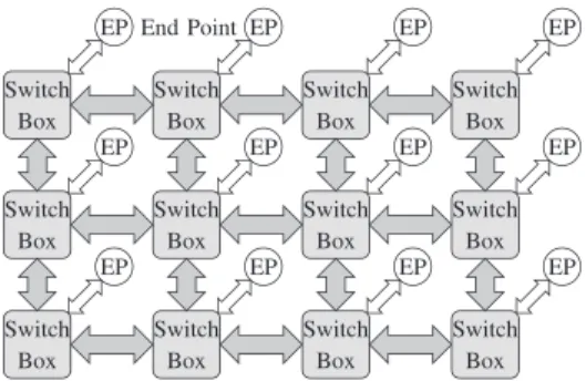
IELD programmable interconnection networks (FPINs) are the backbone of field programmable gate arrays (FPGAs), prototyping platforms [1]–[4], and network-on-chip architectures [5]. Most hardware functions can be emulated in FPGAs by re-programming their embedded FPIN [6], [7]. Hardware systems used for logic emulation can enhance their capability and performance by having multiple FPGAs con-nected together [8]. Fig. 1 illustrates an example where an FPIN provides programmable interconnections between endpoints (I/O or configurable logic blocks) in an FPGA.An active reconfigurable platform was proposed in [9]. It is intended to be an alternative to PCBs for providing intercon-nections among multiple integrated circuits (ICs) for testing and prototyping of an electronic system. This active reconfigurable platform can be seen as an active silicon interposer with an inter-connection network that can be dynamically configured like an FPGA. The active reconfigurable platform has an unidirectional switch box based FPIN that can be programmed by the user to Manuscript received April 15, 2015; revised July 27, 2015; accepted Au-gust 11, 2015. Date of current version September 25, 2015. This research was partly supported by Gestion Technocap, the Natural Sciences and Engineering Research Council of Canada and by the Mitacs program. This paper was rec-ommended by Associate Editor V. Chandra.
The authors are with Polytechnique Montréal and Université du Québec á Montréal (UQAM) (e-mail: [email protected]; blaquiere. [email protected]; [email protected]).
Digital Object Identifier 10.1109/TCSI.2015.2476297
Fig. 1. Generic model of an FPIN in an FPGA.
interconnect the component ICs. It is primarily designed to pro-vide digital interconnection between component ICs randomly and manually deposited on its active surface. However, this plat-form cannot support open-drain bidirectional buses where the direction is embedded in the protocol, as found in the pro-tocol and its derivatives [10]–[13].
Open-drain connections have the unique ability to
simultane-ously support multiple drivers on a single physical node. Unlike
CMOS driver logic, there is no possibility of undefined state in open-drain connections. Indeed, no matter how many I/Os are connected to the bus, if only one of them outputs a LOW on the bus, the bus will become LOW. Open-drain connections are not advantageously used internally in ICs, due to their static power dissipation and relatively low speed. However, they are commonly used to interconnect several ICs, because they usu-ally require fewer IC pins for serial communications between ICs. Multi-master bidirectional buses cannot be implemented by CMOS drivers, because having multiple CMOS drivers driving a single physical node can give rise to undefined voltage levels on the bus. By contrast, multi-master bidirectional buses can be realized by open-drain connections, e.g., and its deriva-tives [12], [13]. This work was motivated by the observation that FPINs based on unidirectional switch boxes cannot support open-drain bidirectional connections.
This paper presents an interface for FPINs to support proto-cols that demand open-drain (or open-collector) connections. The proposed interface can link multiple external signals through the FPIN, while imitating the behavior of open-drain (or open-collector) connections. That interface allows con-necting together arbitrarily large number of pins, subject to delay limitations. To the best of our knowledge, no comparable interface circuit mimicking the behavior of an open-drain con-nection has been reported in the literature. The closest existing circuits that we found are the P82B96 [14] and PCA9600 [15], two commercial bus extension buffers. Even though these circuits are not equivalent to the proposed interface, they have some similarity in their use of double interpretation of voltage 1549-8328 © 2015 IEEE. Personal use is permitted, but republication/redistribution requires IEEE permission.
Fig. 2. Hierarchical description of the active reconfigurable platform, from system level to configurable I/O (CIO).
levels below 0.3 to avoid a state-latching phenomenon (explained in Section III-B).
Section II provides some background on an FPIN-based ac-tive reconfigurable platform and open-drain buses. Section III describes the proposed interface and presents a delay model that can be used to design the interface unit according to com-munication speed specifications. Section IV presents measure-ment results from a test-chip that was implemeasure-mented. Finally, Section V concludes the work by summarizing our main con-tributions and key observations.
II. BACKGROUND
A. Active Reconfigurable Platform [9]
The core of the active reconfigurable platform is a wafer scale IC upon which component ICs are to be deposited. The surface of the wafer scale IC has a dense array of very fine (tens of mi-crometers) conducting pads acting as configurable I/Os (CIOs), as shown in Fig. 2. An FPIN is embedded in the wafer scale IC. The FPIN can be configured, similar to an FPGA, to connect any two CIOs. User specified ICs are to have physical contacts with the CIO and communicate through the embedded FPIN. Each CIO has its own configurable I/O buffers. If a CIO is to operate as an input, then the respective CIO is configured as an input and this buffer receives the signal from a source IC and propagates it through the FPIN to the destination CIO. The des-tination CIO's I/O buffer is configured as an output buffer and it propagates the signal to the destination IC.
B. Open-Drain Connection Based Communication
The protocol is a popular communication standard. It is a bidirectional multi-master serial bus developed by NXP Semi-conductors (formerly Philips SemiSemi-conductors). It uses open-drain connections. is used in various control architectures such as the System Management Bus (SMBus), the Power Man-agement Bus (PMBus), the Intelligent Platform ManMan-agement Interface (IPMI), the Display Data Channel (DDC), and the Ad-vanced Telecom Computing Architecture (ATCA) [10]–[13].
uses two bidirectional open-drain (or open-collector) lines named Serial Data Line (SDA) and Serial Clock Line (SCL), shown in Fig. 3. SDAs and SCLs of all components are respectively connected together. Both lines have external pull-up resistors. The protocol has no explicit signal to specify the direction of data transfer in the bus. Rather, there are some rules embedded in the protocol, like clock
synchro-nization, arbitration, and clock stretching [11] by which all
the ICs connected to a bus determine when they are supposed to write into the bus, read from the bus or stay idle. All those rules are based on the “wired-AND” property of open-drain connections.
Fig. 3. Example of an -bus configuration.
Fig. 4. Each circle represents an interface unit circuit. (a) The star topology. (b) The ring topology.
III. PROPOSED ARCHITECTURE OF THE BIDIRECTIONALINTERFACE
An open-drain bidirectional interface unit is proposed here by the authors. It is designed to meet the following criteria:
• Be compatible to an unidirectional switchbox based FPIN. Minimizes modifications to an existing FPIN, i.e., the in-terface circuit should be integrated at the I/Os of the FPIN; • Imitate the behavior of a single metal line for open-drain (or open-collector) connection where the direction of the signal is automatically detected;
• Allows interconnecting several open-drain I/Os together. Each interface unit has an input and an output through which several interface units can be interconnected in a pre-defined interconnection topology.
A bidirectional interface based on a star topology was previ-ously proposed by the authors [16]. In that topology, each inter-face unit directly communicates with all the others. This leads to the simplest design when a small number of pins need to be connected. Direct connections also minimize delays. However, the star topology has an interconnection complexity of for interface units. For instance, the case where five interface units are interconnected in a star topology is shown in Fig. 4(a). It shows that each interface unit is directly connected with the other four. In the case of the active reconfigurable platform [9], these connections are done through the FPIN. In this platform, the logic connected to a pin can receive at most 24 incoming sig-nals through the FPIN, implying that at most 25 interface units can be interconnected together.
As an complexity gets very expensive when grows, and to overcome the limit on the value of due to the fan-in of the unit cells, a topology with an complexity was devel-oped and is reported in the rest of this paper. That new intercon-nection topology is structured as a ring, as shown in Fig. 4(b). Mimicking the behavior of open-drain (or open-collector) con-nection through a digital FPIN may lead to a state-latching phe-nomenon. This can be explained by a minimal example of two interface circuits defining a minimal solution proposed in Sec-tions III-A and III-B. That minimal solution was enhanced and
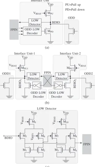
Fig. 5. Development of the bidirectional interface unit circuit. (a) Proposed bidirectional interface. (b) Two interface units interconnected together through an FPIN. (c) The LOW Detector to remove the latching problem.
adapted to a star topology by the authors in [16]. In this paper, the minimal solution described in Sections III-A and III-B is enhanced and adapted to the ring interconnection topology in Sections III-C and III-D.
A. Working Principle of the Bidirectional Interface
When a group of open-drain drivers (ODDs) are to be in-terconnected by a FPIN, instead of being physically connected by a wire, each ODD output has physical connection with the BDIO node of only one interface unit. BDIO denotes the phys-ical node that acts as the bidirectional input and output node of the interface unit. Thus, each interface must be able to sense the voltage on the respective ODD, in order to interpret the infor-mation it conveys and send it to the other interface units through the FPIN. A tentative schematic of the interface unit is shown in Fig. 5(a). Instead of a pull-up resistor (used in [11]), a pull-up pMOS is used ( is a biasing voltage that enables the pull-up pMOS). As will be shown, when such interface units are interconnected through a FPIN, the resulting group of I/Os can emulate an open-drain bus if the LOW Detector and ODD
LOW Decoder modules are suitably designed.
In order to understand the rationale of how the proposed cir-cuit operates, let us first consider the case where only two such interface units are connected through a FPIN, as shown in Fig. 5(b). In that case, each interface unit’s ODD LOW Decoder re-ceives signals from the other interface unit through the FPIN to
TABLE I
PULL-DOWNCURRENT OFOPEN-DRAINBUSES
determine whether the other interface units ODD is outputting a LOW. The LOW Detector module detects the voltage level at its own BDIO node and sends that information to the other in-terface unit. When there are only two interconnected inin-terface units, a NOT-gate can serve the purpose of ODD LOW Decoder and a simple digital buffer can serve as a LOW Detector. When none of the ODD outputs LOW, voltage levels of both BDIOs are held at by their respective pull up pMOS. Thus, both BDIOs send HIGH to each other and the respective internal pull-down nMOS remain OFF, in which case the BDIOs con-tinue to be held at .
Standard drivers can sink several milliamperes (Table I). The pull-up pMOS ( in Fig. 5(a)) is sized so that the pull-up current is less (approximately one-third) than the pull-down cur-rent of standard open-drain drivers (e.g., the protocol and its derivatives). Thus, when one of the ODD outputs a LOW, the corresponding BDIO becomes LOW. Let us assume ODD1 outputs LOW in Fig. 5(b) and is made LOW. It is also assumed that ODD2 is not outputting a LOW. Since
is LOW, LOW logic value will be sent through the FPIN to
Interface Unit-2. That LOW is made HIGH by the NOT-gate
that turns ON the internal pull-down nMOS of Interface Unit-2. Thus, is made LOW, even though ODD2 is not driving it LOW. The opposite would have happened if instead of ODD1, ODD2 outputs LOW.
B. State-Latching Phenomenon
The bidirectional interface shown in Fig. 4 and the minimal circuit example in Fig. 5 suffer from a state-latching problem. Indeed, when becomes LOW, it will also send a LOW signal through the FPIN to Interface Unit-1, and the internal pull-down nMOS of Interface Unit-1 will also turn ON. Thus, when ODD1 turns OFF, the voltage level of will be held LOW by the internal pull-down nMOS of Interface Unit-1 and will not be pulled up to .
The approach taken to solve that latching problem in [16] was to break the latching loop. This was done by defining two distinct voltage levels for the LOW logic value on the BDIOs (Table II). In the protocol, (the allowed maximum voltage level to represent a LOW logic value) is
[11]. At this point, we introduce two reference voltages, named
and , both of which are below (these
two voltages will be generated by a resistor-divider elaborated in Fig. 10). When the BDIO is pulled down by an ODD, the voltage level is pulled down to a value that is below . The pull-down nMOS (and pull-up pMOS) is designed in such a way that when it pulls the BDIO down, the voltage level is pulled down to a value of that is above .
In that case, a comparator circuit such as the one proposed in Fig. 5(c) can have different logical interpretations between a LOW logic value driven by an ODD and the one driven by the internal pull-down nMOS. However, a standard bidi-rectional bus would interpret both voltages as a LOW logic
value, i.e., . This allows breaking
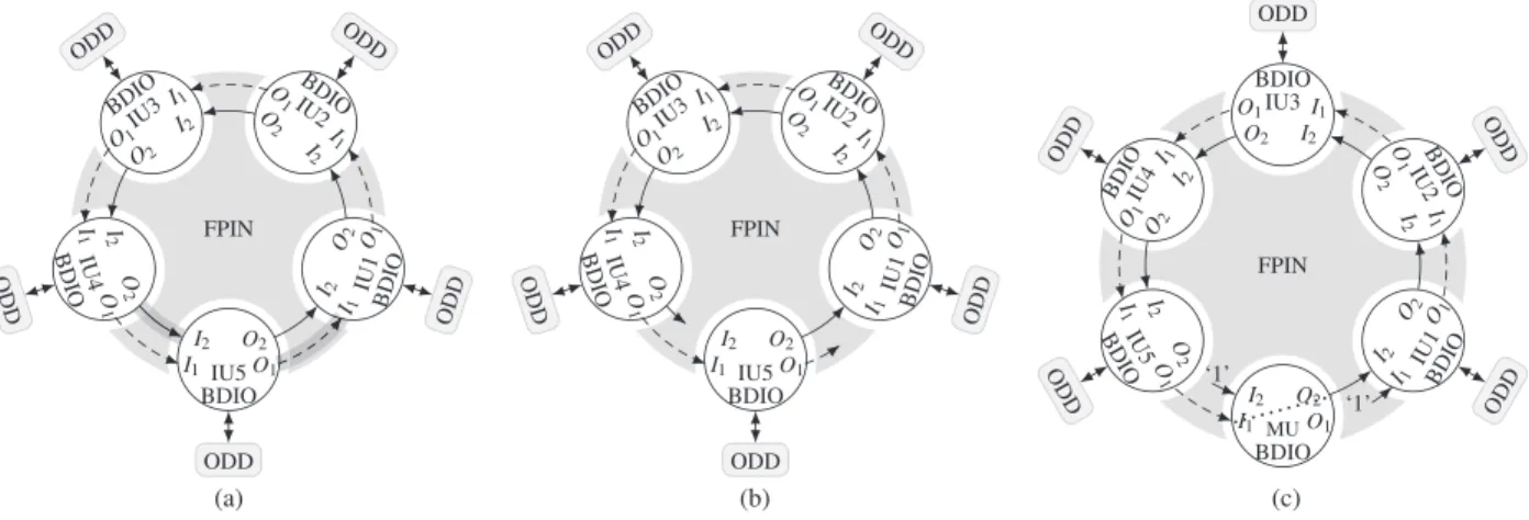
Fig. 6. Development of pseudo-ring interconnection topology. Each circle represents an interface unit circuit and is labelled IU#. (a) First step. (b) Second step. (c) The pseudo-ring interconnection topology.
TABLE II
DIFFERENT STATES WITH RESPECT TO THE
VOLTAGELEVEL OF THEBDIO NODE
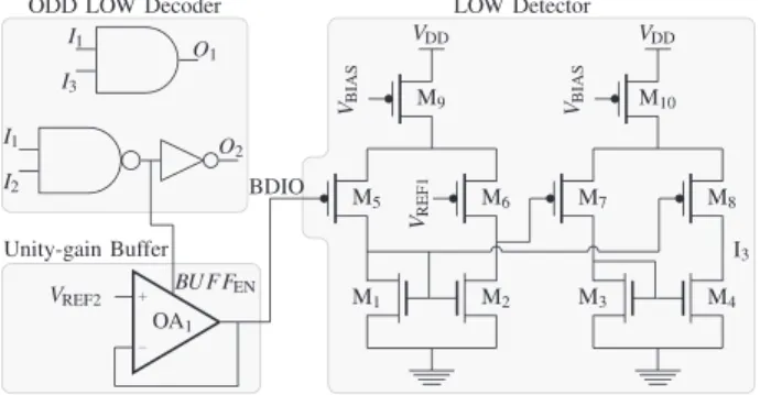
in Fig. 5(b). The desired functionality is obtained with a differential pair , shown in Fig. 5(c). The second differential pair is used only for amplification and level shifting purpose to make the whole circuit robust against process variations. When the voltage at the BDIO is below ( can be considered as the tripping voltage of the differential pair), the LOW Detector will send LOW, else it will send HIGH to other interface units.
Let us reconsider the circuit of Fig. 5(b) where the circuit of Fig. 5(c) is used as LOW Detector. Assuming ODD1 outputs
LOW to , the voltage of drops below
and Interface Unit-1 sends a LOW signal to the ODD LOW
Decoder of Interface Unit-2 through the FPIN. As a result, the
internal pull-down nMOS of Interface Unit-2 is turned ON and the voltage level of is pulled down to that is interpreted as LOW by ODD2. However, since that voltage level is not below , Interface Unit-2 does not send LOW to
Interface Unit-1 and the internal pull-down driver of Interface Unit-1 does not turn ON. Subsequently, when ODD1 releases
, the voltage level of will be pulled up to without any unambiguity, and the state-latching phenomenon is avoided. Thus, the two interconnected interface units imitate the behavior of an open-drain bus, even though internally the BDIOs are loop-connected through the FPIN but not by any direct metal line.
C. The Ring-Interconnection Network of the Bidirectional Interface
Similar to the minimal example in Section III-A and III-B, each interface unit in a ring (Fig. 4(b)) can be in one of three conditions (see Table II) depending whether:
1) the ODD directly connected to the interface drives LOW; 2) another ODD connected to an interface that is part of the
same network drives LOW;
3) none of the ODD drives its interface LOW.
Thus, the same LOW Detector module of Fig. 5(c) can be used to differentiate between a LOW logic value driven by a ODD and the one driven by the internal pull-down nMOS in each in-terface unit. However, in a ring-interconnected topology, each interface unit can communicate with only one other interface unit if implemented as shown in Fig. 5. Hence, the ODD LOW
Decoder module has to be enhanced to communicate these three
conditions to the next interface unit in a ring. Considering the three conditions that each interface must support and communi-cate, at least two bits of information must be communicated in a digital implementation to unambiguously differentiate between the three possible conditions.
A consideration that influences the solution proposed next is the fact that the prototyping platform [9] for which this is elab-orated offers a very large number of configurable digital inter-connects. A possible first step toward a feasible ring-structure solution is to establish two separate rings, as shown Fig. 6(a). For clarity, each interface unit participating in an emulated bidi-rectional bus is labelled as IU#. In the proposed design, a first ring (dashed ring) could communicate whether one or more of the ODDs are outputting a LOW, while the second ring (solid ring) would act upon the information broadcasted by the first ring, to propagate an internal pull-down driver activation signal accordingly. As the two rings constitute closed loops, if any ODD connected to an interface unit (Fig. 6(a)) outputs a LOW, assuming that all interface units are exactly the same, that in-formation would be sent to the subsequent interface units and it would indefinitely circulate through the two rings. This would give rise to a state-latching phenomenon conceptually similar to the one described in Section III-B.
A possible second step toward a practical solution is to break the two rings, as shown in Fig. 6(b), to prevent this unwanted endless circulation. Since the second ring is to act upon the in-formation propagated by the first ring, the two broken rings must be connected together. That role is played by an additional inter-face unit, called the master unit (labelled MU in Fig. 6(c)). The resulting topology, shown in Fig. 6(c), is called a pseudo-ring. Assuming suitable logic and interfacing circuits can be elabo-rated, this solution, first proposed here, would offer in-terconnection complexity, and ODD LOW-Decoder com-plexity. In this topology, each interface unit, with the exception of the MU, is connected to an external ODD through the corre-sponding BDIO.
Fig. 7. Logical signal flow diagram. Low Detector module of each interface unit (IU#) is labelled LD. Each BDIO node belongs to the respective interface unit (IU) and represents distinct physical nodes. (a) Pseudo-ring interconnection topology. (b) Modified pseudo-ring interconnection topology. (c) Signal flow of queue-interconnection topology.
The target prototyping platform is a completely regular struc-ture, thus our objective was to come up, if possible, with a de-sign where the MU could be derived by configuring differently the same logic as in the other IUs. This was found possible if as in Fig. 6(c), IU1 and MU receive a predetermined logic value at their and input respectively. The dashed ring path passing through the and terminals of all interface units, from IU1 to MU, propagates the information whether one or more ODD are outputting a LOW to their respective BDIO. The solid path passing through and form a signal path propagating from MU to IU5 in Fig. 6(c). The path propagates the internal pull-down driver activation signal. MU acts as a bridge between these two signal paths. Each interface unit has an internal bit (called ) that becomes LOW when the voltage level at the re-spective BDIO drops below . The voltage level drops below if and only if the external ODD pulls it down, while it drops to if the internal driver pulls it down.
The logical relations between these binary variables in each interface unit are
(1) Applying (1) to Fig. 6(c), we get the logical signal flow diagram of Fig. 7(a). From Fig. 7(a), we get for any (subscript denotes the variable belonging to IU , and MU denotes the variable belonging to module MU)
(2)
Thus, it can be seen that ( in Fig. 7(a)) is the equivalent “wired-AND” logic implementation of an open-drain connection. Applying (1) to Fig. 7(a), we get,
(3) Thus, the path propagates the “wired-AND” logic value to all interface units and can be used to activate/de-activate their respective internal pull-down drivers. Equation (3) also proves that when all the ODDs output a HIGH logic value to their respective BDIOs by releasing the BDIO nodes, the path will unequivocally begin to propagate a HIGH logic value and hence the aforementioned state-latching phe-nomenon is prevented.
The path propagates the accumulated AND of all and hence the AND operation of along the path does not change the logical value that propagates along the
path ((3)). Thus, using a digital buffer in the path would have sufficed. However, the interface unit has been developed to be integrated in each unit cell of the active reconfigurable platform [9]. Remarkably, the same cell can also be used as the
Master unit (MU in Fig. 7) when necessary by utilizing an
un-used interface unit from an unun-used unit cell. Hence, instead of a digital buffer, an AND-gate was used in the path.
Fig. 8. Logical signal flow diagram of dual-queue interconnection topology. Two individual queue network are joined together. Each queue network have five interface units. Four interface units (labelled IU#) are connected to external ODD and one Master unit (labelled MU). Low Detector module of each interface unit (IU#) is labelled as LD.
At first glance, using MU may seem redundant, because we could have connected to directly. However, using a
Master unit (MU) gives us the ability to interconnect two such
networks. This allows halving the worst case propagation de-lays (analysis elaborated in Section III-D).
D. Queue and Dual-Queue Interconnection Topologies
The previous design outlined in Fig. 6(c) achieves the desired interconnect complexity. But the signal goes around the loop twice. This section calculates the propagation path length and hence, shows how the corresponding delay can be halved. Indeed, according to (3), the AND operation of along the path does not change the logical value that propagates along that path. The functionality would thus be preserved if the direction of signal propagation on the path is re-versed clockwise as shown in Fig. 7(b). If the ring-like struc-ture of Fig. 7(b) is unrolled, it becomes a queue, as shown in Fig. 7(c). This organization is called the queue interconnection topology. Similar to the pseudo-ring topology, whenever one or more ODD outputs a LOW, that LOW propagates through the
path and MU passes that LOW to the path. The unused of MU can also be used to propagate a LOW
to the path from the path of another queue
network to activate the internal pull-down drivers. Hence, the unused and of MU in a queue network can be used to connect two individual queue networks together, as shown in Fig. 8. If one or more ODD of Queue Network-1 outputs a LOW, that LOW will propagate through the path of the Queue
Network-1 and will then pass through MU1 to the path of Queue Network-1 and path of Queue Network-2. Similarly, if one or more ODD of Queue Network-2 outputs a LOW, that LOW will propagate through the path of
Queue Network-2 and will pass through MU2 to the
path of Queue Network-2 and then to the path of Queue
Network-1. Thus, two individual signal paths are established by MU1 and MU2 that propagate LOW and HIGH to each other when necessary and hence, imitates the wired-AND logic of open-drain connection.
In a queue interconnection topology, the signal propagates through the entire length of and path (thick gray line in Fig. 7(c)). By contrast, in the dual-queue interconnection topology, interface units are divided equally in two groups. In this case, the signal propagates through the individual
and paths only (solid and dotted thick gray lines in Fig. 8). After reaching MU1 in Fig. 8, the signal propagates simultaneously along the path of Queue Network-1 (dotted line) and the path of Queue Network-2 (solid line). Thus, the worst case propagation delay in halved in the dual-queue interconnection topology.
Fig. 9. Schematic of the interface unit (IU).
E. Proposed Bidirectional Interface
Based on previous proposals, considerations and discussions, it is now possible to propose an implementation for a bidi-rectional interface that can interconnect several bidibidi-rectional open-drain I/Os in pseudo-ring, queue or dual-queue topology through a FPIN. The schematic of the interface unit is shown in Fig. 9.
According to (3), (or ) propagates the “wired-AND” logic value. Hence, is used to activate/deactivate the
Unity-gain Buffer in Fig. 9. In fact, is used because the Unity-gain
Buffer is activated when a HIGH value is applied as . Upon activation, the Unity-gain Buffer propagates to the BDIO node. When deactivated, the Unity-gain Buffer in Fig. 9 outputs 3.3 V by a pull-up pMOS to the BDIO node and hence, the Unity-gain Buffer is acting as the internal pull-down driver as well as the pull-up pMOS.
When the external ODD outputs a LOW, the voltage at the
BDIO falls below and is made LOW by the LOW
Detector. ODD LOW Decoder represents the logical behavior
among , , , , and of the interface units shown in Figs. 7, 8, and 9. Hence, the interface unit of Fig. 9 can be in-terconnected in the pseudo-ring, queue or dual-queue intercon-nection topologies and will imitate the “wired-AND” logic of open-drain buses.
F. Propagation Delay of Dual-Queue Interconnection Topology
A propagation delay model is developed for the dual-queue topology in this subsection. Only this topology is analyzed because it has the lowest (best) propagation delay. Similarly, delay models can be developed for the pseudo-ring and queue topology. At this point, we establish a notation system to denote delays and rise/fall times associated with various circuit components or path segments in the entire propagation path. is used to denote various delays and is used to denote rise/fall times. Subscripts have two indices. The first index denotes the logic value to which the delay corresponds. The second index denotes the interface unit or path segments to which the
TABLE III
DELAYS ANDRISE/FALLTIMES OF THEINTERFACECIRCUIT
delay or rise/fall time belongs to. For example, the worst case propagation delay for LOW and HIGH logic value is denoted
by and respectively.
The worst case signal propagation path of the dual-queue net-work is shown by the solid thick gray line in Fig. 8. The path begins at IU1 and ends at IU8 (IU in general). The worst case propagation delay can be divided in three delay segments:
1) The first delay segment is associated with the interface unit (IU1) to detect the voltage transition at the BDIO node and
encode that information to be sent to other interface units.
It is called the detection delay ( or ).
2) The second delay segment is associated with the transmis-sion of that encoded information through
path. It is called the transmission delay ( or ). 3) The third delay segment is associated with the decoding of
that information and subsequent activation of the internal pull-down driver of IU8. It is called the activation delay
( or ).
Thus worst case propagation delays for the dual queue topology can be expressed as
(4a) (4b) Each of the aforementioned three delay segments consists of one or multiple circuit component delays. For example, when ODD is activated, it takes some time to bring down the voltage level from HIGH to LOW. Subsequently, the LOW Detector (LD in Fig. 8) will require some time to detect the LOW logic value at the BDIO node and produce a LOW logic value at . After that, the LOW logic value propagates through the path. This path consists of AND-gates of
ODD LOW Decoders. All these AND-gate delays are
catego-rized in Table III. The definition of these delays will be gradu-ally introduced in the following explanation. At this point, we introduce the signal propagation path as superscript in the delay term to denote the component to which the delay term belongs to. For example, denotes the LOW logic value prop-agation delay of the AND-gate from to in IU2. Since Table III categorizes the various circuit component delays, the second index in the subscript of the delay or rise/fall time is kept empty.
1) LOW Logic Propagation Delay: The worst case
propaga-tion path for LOW logic value begins from the ODD connected to IU1. The first delay is the time ( ) required by the ODD to bring the voltage level from HIGH to LOW at the BDIO node of IU1. is defined as the time required
by the ODD to bring the voltage level of the BDIO node from to . Then the LOW Detector (LD in Fig. 10) of IU1 will require some time ( ) to detect the LOW logic value at the BDIO node and produce a LOW logic value at . is measured only between the crossing of by the voltage of BDIO node and the HIGH-to-LOW transition in because to transition depends on the ODD (ex-ternal driver). Then the LOW logic value will propagate through the AND-gate of IU1 from to . Together, these three delays constitute .
(5) Then the LOW logic value begins to propagate from IU1 along the signal path through FPIN to MU1, then to MU2, and then along the signal path through the FPIN to IUn (IU8 in Fig. 8). These delays constitute the worst case transmission delay . Thus,
(6) Finally, after the LOW logic value reaches IU8, the internal pull-down driver of IU8 is activated and it requires some time to bring the voltage level of the corresponding BDIO node from
to . in Table III is defined as the time
needed by the internal pull-down driver to bring the voltage
level of the BDIO node from to . Thus,
(7)
2) HIGH Logic Propagation Delay: The worst case
propa-gation path for HIGH logic value is the same as for the LOW logic value. The propagation begins with the deactivation of the ODD connected to IU1. However, in this case, the voltage of the BDIO node does not have to rise from LOW to HIGH for the
LOW Detector to detect it. In fact, the voltage level of the BDIO
node is required to rise from 0 V to (approximately 10% of ) for the LOW Detector to begin to detect. Hence, in Table III is defined to include that rise time and the delay of the LOW Detector itself. is the delay be-tween the deactivation of the ODD (external driver) and the corresponding LOW-to-HIGH transition of . Then the HIGH logic value propagates through the AND-gate of IU1 from to
. Together, these two delays constitute .
(8) Similar to , the HIGH logic value propagates from IU1 along signal path through FPIN to MU1, then to MU2, and then along signal path through FPIN to IUn (IU8 in Fig. 8). These delays constitute the worst case transmission
delay . Thus,
(9) Finally, after the HIGH logic value reaches IU , the internal pull-down driver of IU8 is deactivated and it requires some time to bring the voltage level of the corresponding BDIO node from
Interconnection Topology
In principle, an arbitrarily large number of interface units can be interconnected by the dual-queue topology. In practice, the maximum number is limited by the worst case propagation de-lays of the LOW/HIGH logic value and the required commu-nication speed of the supported open-drain protocol. The worst case propagation delays of the LOW and HIGH logic value are equivalent to the fall and rise time respectively of the target communication speed specification. From ((4a), (5)–(7)), the worst case propagation delay of the LOW logic value in the dual-queue network includes the fall-time of two BDIO nodes
( in and in ). From ((4b),
(8)–(10)), the worst case propagation delay of a HIGH logic value in the dual-queue network includes the rise-time of only one BDIO node ( in ). Thus, (4a) represents the
critical path that puts a practical limit on the maximum BDIO
node capacitance and the maximum number of interface units that can be interconnected with the dual-queue topology to sup-port a required communication speed.
All I/Os are physically connected together in a conventional communication, thus the total bus capacitance is the sum-mation of all I/O capacitances and interconnecting wires. It re-sults in a value that can get fairly large. According to spec-ifications (fast-mode plus), a standard value of the bus capaci-tance is 400–550 pF and the maximum fall-time is 120 ns [11]. However, when interconnected through the proposed bidirec-tional interface, each driver is to be directly connected to the BDIO node of only one interface unit, as shown in Fig. 8. Hence, standard drivers can achieve a shorter rise/fall times. For ex-ample, if the loading capacitance of the BDIO node is one-fifth of the standard bus capacitance, then standard drivers (ODD) would achieve one-fifth of their normal fall-time. Similarly, the internal pull-down driver, if designed according to the standard, can also achieve a fall time that is a frac-tion of the fall-time. Thus, with proper design, both and can be made equal to a pre-determined fraction of a normal fall time.
and represent a deterministic amount of delay because those depend only on IU1 and IU respectively. How-ever, accumulates as the number of interconnected inter-face units increases. Thus, components associated with
and can be designed so that and consume a
deterministic fraction of the fall-time for any given commu-nication speed. Thus, could consume the remaining ‘un-used’ part of fall-time. Timing constraints will thus im-pose limits on the number of ODDs that could be intercon-nected by a set of interface units conintercon-nected using the dual-queue topology that would maintain the worst case propagation delay to be less than or equal to the maximum fall-time of a regular
connection.
Of course, a smaller loading capacitance of the BDIO node or stronger internal drivers would result in smaller rise/fall times. It would leave more headroom for or . Thus, larger number of ODDs could be interconnected by the interface units with the dual-queue topology while meeting a given communi-cation speed.
a lower power supply) to leverage their high speed.
A. Design Specification of the Bidirectional Interface
A detailed transistor level schematic of the interface unit is shown in Fig. 10. The LOW Detector has physical connection with the configurable I/O (BDIO node) and hence was designed with thick-oxide 3.3 V I/O FETs, as shown in Fig. 10. and are 3.3 V logic signals. If the voltage level of the
BDIO node falls below , and become LOW and
HIGH respectively. The interface units are to communicate among themselves through the embedded FPIN. Thus, the logic function among , , , , and were implemented in 1.2 V 2.2 nm-oxide FETs. Thus, the voltage levels of and were brought down to 1.2 V by a down-converter (
in Fig. 10). and are logically equivalent. On the other side, and are 1.2 V logical signals. Thus, an up-converter ( in Fig. 10) was used to convert the from a 1.2 V signal to a 3.3 V signal that is used to activate the Unity-gain
Buffer in Fig. 10. The Unity-gain Buffer that has physical
connection with the I/O was designed with thick-oxide 3.3 V I/O FETs. A resistor divider was used to generate and . Finally, the Unity-gain Buffer was used to propagate
to the BDIO node.
Section III-G provides guidelines to use the delay model of Section III-F to design the various components of the interface unit to support a given communication speed. The prototype bidirectional interface was designed to support fast-mode plus specifications (Table IV). The amplifier of the Unity-gain
Buffer was designed to provide a pull-down current of 0.53 mA
and a pull-up current of 1.2 mA for a loading capacitance of 15 pF. It can achieve a fall-time ( in Table III) of 90 ns. Since the loading capacitance of 15 pF at each node is one-thirtieth of the standard bus loading value of 400–550 pF [11], a standard fast-mode plus driver can achieve a fall-time ( in Table III) of 4 ns. The AND-gates of the ODD LOW Decoders were designed to have a delay that is a fraction of a nano second in the target CMOS technology. With these tentative values and the delay model of Section III-F, a few tens of such interface units can be interconnected using the dual-queue topology and the worst case propagation delay of such a network would be less than 120 ns. Since the interface imitates the behavior of an open-drain or open-collector bus, it can be redesigned with different parameters (e.g., different
values of , , , , , ) for other
communi-cation speeds.
B. Delay Characterization of the Bidirectional Interface from Post-Layout Simulation
In the test-chip, only the BDIO node of the interface units could be measured. Thus, only the total propagation delay be-tween two interface units could be derived from measurements. Since every point inside the test-chip could not be measured, in-dividual delays of the ODD LOW Decoder and LOW Detector, as well as the rise/fall time of the Unity-gain Buffer (internal pull-down driver) and the ODD were derived from post-layout
Fig. 10. Detailed transistor-level schematic of the bidirectional interface unit and microphotograph of the die. TABLE IV
DESIGNSPECIFICATION OF THEBIDIRECTIONALINTERFACE IN THETEST-CHIP
ACCORDING TO FAST-MODEPLUSPROTOCOL
As the test-chip is to be used to validate the concept, the BDIO node capacitance value was chosen to include the PCB trace, oscilloscope probe and connecting wire, and pad capacitances only.
simulations. Table V summarizes the numerical values of var-ious component delays and rise/fall times of the interface unit based on post layout simulations. These values indicate that in a network comprising less than 10 interface units, the total propagation delay will be primarily dominated by , , and . These three delays constitute the detection delays ( or ) and the activation delays ( or ). Various delays of the ODD LOW Decoder
module ( , , , etc.) that constitute the
transmission delay ( or ) are almost negligible com-pared to the aforementioned three delays. Thus, their effect on the total propagation delay is very small. Contributions of all these individual component delays on the total propagation delay of HIGH/LOW logic values between two interface units will be compared with measured propagation delays from the test-chip in Section IV-D.
TABLE V
CHARACTERIZATION OF THEINTERFACECIRCUIT
BASED ONPOSTLAYOUTCIRCUITSIMULATIONS
This delay is not a characteristics of the interface unit but of the test-bench.
Replacing the right hand side of (4a) and (4b) with the elab-orated expressions of (5)–(10) gives the worst case propagation delays of the LOW and HIGH logic values in terms of the dividual component delays and rise/fall times. Subsequently in-jecting the corresponding values from Table V in (4a) and (4b), we get in nanosecond (ns):
(11a) (11b) when each pin (BDIO) has a load capacitance of 15 pF and is the number of interconnected interface units.
C. Test-Chip and Test-Bench Specifications
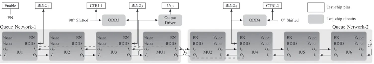
A test-chip was fabricated using IBM 0.13 CMOS tech-nology. A dual-queue interconnected network prototype shown in Fig. 11, that consists of eight interface units was fabricated in this test-chip. A photomicrograph of that test-chip is shown in Fig. 10. A Tektronix MDO4014-6 oscilloscope was used to observe the voltage waveforms. TEKTRONIXTPP1000 passive probes were used. They introduce a 4 pF parasitic capacitance.
Fig. 11. Dual-queue interconnection topology with 8 interface units implemented in the test-chip.
Fig. 12. Measurement result of dual-queue interconnected network (shown in Fig. 11) from the test-chip.
In the test-chip, isolated nMOS were fabricated to act as ex-ternal ODD or drivers designed to be compliant to the fast-mode plus specification summarized in Table I. It should be noted that these drivers are not part of the bidirectional interface units. These drivers are part of the test bench and were added in the test-chip to facilitate the testing operation.
Measured waveform data were extracted from the oscillo-scope and plotted in Fig. 12. They show that the dual-queue in-terconnected network mimics the “wired-AND” logic of open-drain connection. The eight interface units are called IU1 to IU6 and MU1 and MU2 in Fig. 11. ODD3 and ODD4 are operated as drivers. CTRL1, a 1.25 MHz pulse having a pulse width of 400 ns, was applied to ODD3, shown in Fig. 11. CTRL2 is a similar pulse train, left-shifted by 200 ns or 90 , that was applied to ODD4, shown in Fig. 11. Due to the limited number of avail-able test-chip pins, BDIO nodes of IU1, IU2, IU5, and IU6 were not actively driven by ODD. Those interface units could still be assumed to be connected to open-drain drivers that never turn ON. These BDIO nodes are not loaded, but even if they were, such loading would not affect the propagation delay of critical path (solid and dotted thick gray lines) as apparent in Fig. 8.
D. Measurement Results From Dual-Queue Topology With 8 Interface Units
Fig. 12 shows three successful cycles of operation of the implemented bidirectional bus. The cycle beginning at t=1000
ns will be described in detail. It can be seen in Fig. 12 that during the interval between 1000 and 1200 ns, when only ODD4 was activated, the internal drivers of IU3 and IU1 became ac-tivated to produce a LOW logic value ( or 600 mV) at and respectively. During the interval between 1200 and 1400 ns, when both ODD3 and ODD4 were
acti-vated, the voltage level of both and was 0
V, and voltage level of was at that corresponds to the LOW logic value also. During the interval between 1400 and 1600 ns, when only ODD3 remained activated, the internal drivers of IU4 and IU1 remained activated to maintain a voltage
of or 600 mV at and respectively that
corresponds to LOW logic values. Finally, during the interval between 1600 and 1800 ns, when both ODD3 and ODD4 were deactivated, the internal drivers of IU3, IU4 and IU1 became de-activated to produce a voltage of 3.3 V at , , and respectively that corresponds to HIGH logic values. This completes a full validation cycle that begins to repeat at 1800 ns. Thus, the dual-queue interconnected bidirectional in-terfaces successfully mimic the “wired-AND” logic of open-drain connection.
It can be seen in Fig. 12 that the fall time of the nodes and are not equal. This is due to different lengths of PCB traces and the corresponding loading capaci-tances. It should be noted that even though two drivers do not output LOW logic value during normal operations, two drivers can do so when they compete to take control of the bus. has an arbitration process [11] through which such contention is resolved and that arbitration process depends on the wired-AND property of open-drain connection. The interval between 1200 and 1600 ns demonstrates the ability of the proposed interface unit to properly support such a scenario where two drivers simultaneously output a LOW logic value (1200 to 1400 ns) and subsequently one of the drivers output a HIGH logic value (1400 to 1600 ns).
The total propagation path of a LOW logic value from IU4 to IU1 through MU2 and MU1 in Fig. 11 is shown by the thick dashed gray line. This path demonstrates the propagation of a LOW logic value from one individual queue (Queue Net-work-2) to the other queue (Queue Network-1). Comparing var-ious delays and rise/fall times from Table V, can be seen as the largest value. From (4a), (5)–(7) that combines all the individual component delays and rise/fall times associ-ated with the propagation of a LOW logic value, it can be de-duced that would account for more than 95% of the total propagation delay from IU4 to IU1. The voltage wave-form of in Fig. 12 supports that analysis. In Fig. 12 (Label-A), at , after the voltage level of
is brought down to 0 V by ODD4, a LOW logic value propa-gates from IU4 through MU2 and MU1. It reaches IU1 within a
few nanoseconds, and then the internal pull-down driver of IU1
pulls down the voltage level of the node to or 600 mV in 120 ns (Label-B).
V. CONCLUSION
This paper has presented an open-drain interface circuit that can support a bidirectional bus structure using a field programmable interconnection network. An interconnection topology, called dual-queue, has been proposed. The topology has an interconnection complexity of , where is the number of interconnected interfaces. A delay model has been developed for the topology. The model can be used to de-termine the maximum number of interface units that can be interconnected to support a given communication speed.
The proposed interface circuit has been fabricated in a 0.13 CMOS technology and was successfully tested. The inter-connection topology has been validated by measurements from the test-chip. The fabricated circuit has been designed to meet the specification of the fast-mode plus protocol when imple-mented with the active reconfigurable platform of [9]. Neverthe-less, it could be integrated with any FPIN or FPGA. In principle, it can support any open-drain bus with their respective reference voltages.
ACKNOWLEDGMENT
The authors would like to acknowledge CMC Microsystems for the products and services that facilitated this research (CAD tools by Cadence, fabrication services using 0.13 CMOS technology from IBM, and packaging services). This work was partly done while one of the authors was a guest professor at COMELEC-Telecom ParisTech.
REFERENCES
[1] Freescale, Mar. 2014, M68hc11e Family [Online]. Available: http://www.freescale.com/files/microcontrollers/doc/data_sheet/ M68HC11E.pdf
[2] Synopsys, Mar. 2014, Zebu-Server: Billion Gate, Multi-User/Mode ASIC and SoC Emulation [Online]. Available: http://www.syn-opsys.com/Tools/Verification/hardware-verification/emulation/Pages/ zebu-server-asic-emulator.aspx
[3] Mentor, Mar. 2014, Veloce Emulation Systems [Online]. Available: http://www.mentor.com/products/fv/emulation-systems/
[4] Cadence, Mar. 2014, Cadence Palladium Series With Incisive XE Software [Online]. Available: http://www.cadence.com/rl/Re-sources/datasheets/incisive_enterprise_palladium.pdf
[5] Arteris, Apr. 2014, Network on Chip (noc) Interconnect Technology for socs [Online]. Available: http://www.arteris.com/technology [6] Xilinx, Jul. 2015, All Programmable FPGAs and 3D ICs [Online].
Available: http://www.xilinx.com/products/silicon-devices/fpga.html [7] Altera, Jul. 2015, Altera FPGAs [Online]. Available:
https://www.al-tera.com/products/fpga/overview.html
[8] Xilinx, Mar. 2014, 7 Series FPGAs Overview [Online]. Avail-able: http://www.xilinx.com/support/documentation/data_sheets/ ds180_7Series_Overview.pdf
[9] R. Norman, O. Valorge, Y. Blaquiere, E. Lepercq, Y. Basile-Bella-vance, Y. El-Alaoui, R. Prytula, and Y. Savaria, “An active reconfig-urable circuit board,” in Proc. Joint 6th Int. IEEE Northeast Workshop
Circuits Syst. and TAISA Conf. (NEWCAS-TAISA 2008), Jun. 2008, pp.
351–354.
[10] A. Moelands and H. Schutte, “Two-wire bus-system comprising a clock wire and a data wire for interconnecting a number of stations” European eP Patent 0 051 332, Apr. 11, 1984 [Online]. Available: https://www.google.com/patents/EP0051332B1?cl=en
[11] “ -bus specification and user manual,” May 2014 [Online]. Avail-able: http://www.nxp.com/documents/user_manual/UM10204.pdf [12] R. White and D. Durant, “Understanding and using pmbus trade; data
formats,” in Proc. 21st Annu. IEEE Appl. Power Electron. Conf. Expo.
(APEC'06), Mar. 2006, p. 7.
[13] SMBus, SMBus Specifications Mar. 2014 [Online]. Available: http:// smbus.org/specs/smbus20.pdf
[14] “P82B96—Dual bidirectional bus buffer,” Mar. 2014 [Online]. Avail-able: http://www.nxp.com/documents/data_sheet/P82B96.pdf [15] “PCA9600—Dual bidirectional bus buffer,” Mar. 2014 [Online].
Available: http://www.nxp.com/documents/data_sheet/PCA9600.pdf [16] W. Hussain, Y. Savaria, and Y. Blaquiere, “An interface for the
protocol in the waferboard,” in Proc. IEEE Int. Symp. Circuits Syst.
(ISCAS), 2013, pp. 1492–1495.
Wasim Hussain received the B.Sc. degree from Bangladesh University of Engineering and Tech-nology (BUET) in 2008 and the M.A.Sc. degree from Concordia University, Canada, in 2011. Currently he is pursuing the Ph.D. degree at Polytechnique Montréal, Canada. His research interests include low-power/high-speed SRAM design, bidirec-tional communication interfaces, and delta-sigma modulator based A-to-D (both synchronous and asynchronous) conversion.
Yves Blaquiére (M’86) received the B.Ing., M.Sc.A, and Ph.D. degrees in electrical engineering from Ecole Polytechnique de Montréal, Canada, in 1984, 1986, and 1992, respectively, and he is a Professor with Université du Québec á Montréal, Canada (UQAM) since 1987. He works in the field of electrical/electronic/microelectronic engineering, specifically in ASIC/FPGA design, VLSI/WSI microsystems, high speed digital circuits, timing tools, architectures, defect tolerance and applications to signal processing, network/high speed processors, and switches. He did projects in collaboration with several microelectronic companies such as Gestion TechnoCap Inc. DreamWafer Division, Hyperchip Inc. He especially did WSI research with Hyperchip Inc. from 1997 to 2004, including a 2 year period where he contributed full time as technical lead researcher and manager of a team of 35 ASIC/FPGA engineers, to deliver a core internet protocol petabit router. Prof. Blaquiére is a member of the Ordre des Ingénieurs du Québec (OIQ), was director of Laboratoire de recherche de conception en microélectronique at UQAM from 1992–1999 and 2004–2008, director of the Microelectronic Engineering program and Director of Engi-neering at UQAM.
Yvon Savaria (S’77–M’86–SM’97–F’08) received the B.Ing. and M.Sc.A degrees in electrical engi-neering from École Polytechnique Montréal, Canada, in 1980 and 1982 respectively. He also received the Ph.D. degree in electrical engineering in 1985 from McGill University, Montréal, Canada. Since 1985, he has been with Polytechnique Montréal, where he is currently Professor in the department of electrical engineering.
He worked in several areas related to microelec-tronic circuits and microsystems. He is currently in-volved in several projects that relate to aircraft embedded systems, green IT, wireless sensor networks, virtual networks, computational efficiency and ap-plication specific architecture design. He holds 16 patents, has published 122 journal papers, and 385 conference papers, and he was the thesis advisor of 160 graduate students who completed their studies. He has been working as a con-sultant or was sponsored for carrying research by Bombardier, CNRC, Design Workshop, Dolphin, DREO, Genesis, Gennum, Hyperchip, ISR, LTRIM, Mi-randa, MiroTech, Nortel, Octasic, PMC-Sierra, Technocap, Thales, Tundra, and VXP. He is a member of the Regroupement Stratégique en Microélectronique du Québec (ReSMiQ), of the Ordre des Ingénieurs du Québec (OIQ), and was a member of CMC Microsystems board from 1999 to 2014 and chairman of that board from 2008 to 2010. He was awarded in 2001 a Tier-1 Canada Re-search Chair (http://www.chairs.gc.ca) on design and architectures of advanced microelectronic systems. He also received in 2006 a Synergy Award of the Nat-ural Sciences and Engineering Research Council of Canada.