HAL Id: tel-01450671
https://tel.archives-ouvertes.fr/tel-01450671
Submitted on 31 Jan 2017HAL is a multi-disciplinary open access
archive for the deposit and dissemination of sci-entific research documents, whether they are pub-lished or not. The documents may come from teaching and research institutions in France or
L’archive ouverte pluridisciplinaire HAL, est destinée au dépôt et à la diffusion de documents scientifiques de niveau recherche, publiés ou non, émanant des établissements d’enseignement et de recherche français ou étrangers, des laboratoires
photonic applications
Yanping Wang
To cite this version:
Yanping Wang. Structural analyses by advanced X-ray scattering on GaP layers epitaxially grown on silicon for integrated photonic applications. Optics [physics.optics]. INSA de Rennes, 2016. English. �NNT : 2016ISAR0013�. �tel-01450671�
pour obtenir le titre de DOCTEUR DE L’INSA RENNES Spécialité : Physique - Optoélectronique
Yanping WANG
ECOLE DOCTORALE : SDLM
LABORATOIRE : FOTON-OHM/INSA de Rennes
Structural analyses by
advanced X-ray
scattering on GaP
layers epitaxially
grown on silicon for
integrated photonic
applications
Thèse soutenue le 17.06.2016
devant le jury composé de : Gilles PATRIARCHE
Directeur de Recherche CNRS, C2N, Marcoussis / Président
Chantal FONTAINE
Directrice de recherche CNRS, LAAS, Toulouse / Rapporteur
Olivier THOMAS
Professeur des Universités, IM2NP, Université d’Aix-Marseille / Rapporteur
Jean DECOBERT
Ingénieur de Recherche, III-V Lab, Palaiseau / Examinateur
Charles RENARD
Chargé de Recherche, C2N, Orsay / Examinateur
Antoine LETOUBLON
Structural analyses by advanced X-ray
scattering on GaP layers epitaxially grown on
silicon for integrated photonic applications
Firstly, I would like to deeply acknowledge my supervisor prof. Olivier Durand for giving me the opportunity to perform my PhD project in his research group and for his continuous support during my thesis. His precious guidance, advices, pedagogy and encouragements have helped me to fulfill the thesis. I really appreciate his solid knowledge and that he treats everything seriously and methodically, which guided me not only in doing the research, but also in everyday life.
As well, I express my sincere gratitude to my second supervisor Dr. Antoine Létoublon for instructing me in the X-ray diffraction experiments with great enthusiasm. He has shared with me not only his knowledge but also the precious inspiring ideas on research. I’m very grateful to him for his guidance in the world of X-ray diffraction that makes me go forward in the right direction.
I want to thank Chantal Fontaine, Olivier Thomas, Jean Decobert, Gilles Patriarche and Charles Renard for having accepted to be the members of my dissertation committee, for their time, their patience and their critiques during my final defense. A special thanks to Chantal and Olivier for their precise review of the manuscript and providing many valuable comments that improved this dissertation.
I’m thankful to Charles Cornet, for giving me all his patience and precisions when telling me about the sample growth, teaching me use the Atomic Force Microscope, and helping me writing the journal papers. My thanks also goes to Alain Le Corre, Yoan Léger, Laurent Pedesseau, Mickael Coqueux, Julien Lapeyre, Isabelle Eyeillard, Alexandrine Le Saint and all the other colleagues in our laboratory, for giving me their help when I need. It was a great pleasure to pass these years in such a warm and nice group.
I have had the chance to participate in three measurement campaigns at the European Synchrotron Radiation Facility, respectively on the BM02 beamline and on the ID01 beamline. I’m thankful to the staff of the BM02 team and the ID01 team, especially Nathalie Boudet, Jean François Berar, Tobias Tschulli, Gilbert Chahine, Vincent Favre-Nicolin and Joël Eymery, for their help during and after the experiments. I also acknowledge Valérie Demange from ICSR for providing us the access to their X-ray Diffractometer.
Largeau from LPN for the beautiful TEM images, as well as Pascal Turban and Simon Charbonnier from IPR for the STM analyses, without which I wouldn’t have had a thorough understanding of the structure of the GaP epilayer.
Finally, I’m deeply indebted to my parents for their selfless love and unconditional support throughout my whole life and my study.
List of abbreviations ... vii
General introduction ... 1
Chapter 1 Advanced X-ray scattering on crystal defects... 5
1.1 Crystal defects in heteroepitaxial thin layers ... 6
1.1.1 Crystal defects ... 6
a Point defects ... 6
b Linear defects ... 7
c Planar defects ... 8
d Volume defects ... 11
1.1.2 Defects in hetoroepitaxial GaP/Si thin layers ... 11
a Lattice strain of the epilayer ... 11
b Lattice relaxation and misfit dislocation ... 13
c Mosaicity characteristics ... 14
d Antiphase domains and antiphase boundaries ... 15
e Microtwins ... 15
1.2 X-ray scattering in reciprocal space ... 16
1.2.1 Reciprocal space and reciprocal lattice point ... 16
1.2.2 Diffraction conditions ... 17
a Bragg’s condition ... 17
b Ewald Sphere construction ... 18
1.2.3 Reciprocal space map and line profile scans... 18
1.2.4 Pole figure ... 19
1.3 Analysis of heteroepitaxial layers by X-ray scattering techniques ... 22
1.3.1 Determination of epilayer strain and relaxation ... 23
1.3.2 Evaluation of lattice misorientation ... 25
1.3.3 Measurement of layer thickness ... 26
1.3.4 Observation of MTs in reciprocal space ... 27
2.1.1 Vicinal Si substrate ... 30
2.1.2 Si surface cleaning ... 32
2.1.3 Heteroepitaxial growth of GaP thin layers on Si ... 35
2.2 X-ray diffraction setups ... 37
2.2.1 Laboratory X-ray diffraction ... 37
2.2.2 Synchrotron X-ray diffraction ... 39
2.3 Other analytical techniques ... 42
2.3.1 AFM ... 43
2.3.2 TEM and STEM ... 43
2.3.3 STM ... 44
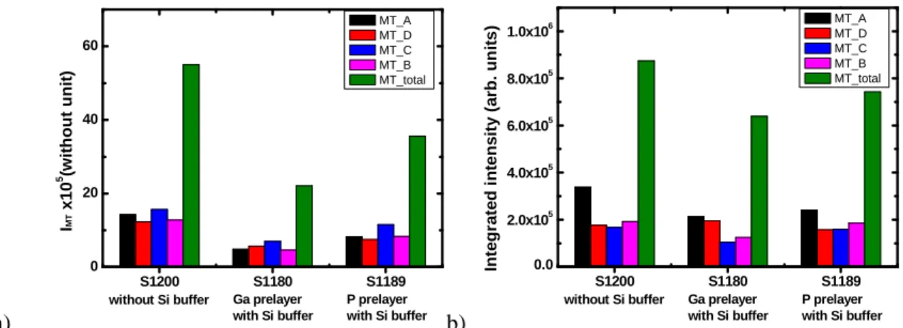
Chapter 3 Quantification of MT density for growth condition optimization ... 45
3.1 Previous MT study on non-optimized GaP/Si samples ... 46
3.2 Development of new quantification methods ... 48
3.2.1 Visualization and evaluation by pole figure method... 48
a Performance of pole figure and visualization of MT ... 48
b Quantification of MT density ... 50
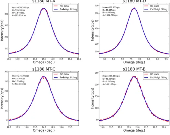
3.2.2 Quantification by rocking-curve method ... 52
3.2.3 Correction of pole figure quantification ... 56
3.3 Growth condition optimization towards the elimination of MT: application of the MT quantification methods ... 57
3.3.1 Growth temperature ... 58
a Reduction of MT density at higher growth temperature ... 59
b Discussion on MT formation and prevention ... 63
3.3.2 Migration Enhanced Epitaxy growth ... 65
3.3.3 Two-step growth sequence ... 67
3.4 Other discussions and comments on the MT formation and quantification ... 69
3.4.1 Anisotropy and influence of the Si surface atomic steps ... 69
3.4.2 Horizontal homogeneity of MT distribution ... 72
4.1.1 RSM recorded on laboratory XRD setup ... 76
4.1.2 Reciprocal space images by synchrotron X-rays ... 79
4.1.3 Transverse scan analysis ... 83
a Quality Factor ... 84
b Williamson-Hall-like plot... 84
4.2 Growth condition optimization towards APB density reduction ... 85
4.2.1 Annihilation of APD at high growth temperature ... 86
a Reduction on APD density evidenced by TEM images ... 86
b Investigation of surface roughness related to APDs ... 88
c APD annihilation using two-step growth sequence ... 90
4.2.2 Limitation of the APD formation at the interface ... 95
a Si surface preparation ... 95
b Ga coverage at the initial growth stage ... 98
c Optimized two-step growth sequence ... 101
4.2.3 APD annihilation by AlGaP marker layers ... 106
4.2.4 Conclusions ... 111
4.3 Discussions and hypothesis on APD annihilation ... 111
4.3.1 Propagation of APBs in low index {11n} planes ... 112
4.3.2 Post-growth annealing ... 113
4.3.3 Growth of main phase GaP over small APDs ... 114
4.3.4 Other important observations and possible interpretations ... 115
4.4 Summary ... 117
Chapter 5 General conclusions and perspective works ... 119
5.1 Summary and conclusions ... 119
5.2 Perspective works ... 122
5.2.1 Attempts of Coherent Bragg Imaging ... 122
5.2.2 Quick scanning X-ray diffraction microscopy ... 127
5.3 Suggestions for future works ... 130
A3 Improvement of the Signal-to-noise ratio for low resolution lab XRD setup ... 134
References ... 135
Résumé de Thèse ... 145
List of abbreviations
AFM Atomic Force Microscopy
APB Antiphase Boundaries
APD Antiphase Domain
BF Bright Field
CL Correlation Length
CMOS Complementary Metal Oxide Semi-conductor
CTR Crystal Truncation Rod
DF Dark Field
DFT Density Functional Theory
EIC Electronic Integrated Circuits
FCC Face Centered Cubic
HAADF High-Angle Annular Dark-Field
HCP Hexagonal Close Packed Structure
IB Integral Breadth
LED Light-Emitting Diode
MBE Molecular Beam Epitaxy
MEE Migration Enhanced Epitaxy
MOCVD Metal Organic Chemical Vapor Deposition
MOVPE Metal Organic Vapor Phase Epitaxy
MT Microtwin
OEIC Optoelectronic Integrated Circuits
QF Quality Factor
r.m.s. Root Mean Square
RC Rocking-curve
RELP Reciprocal Lattice Point
RHEED Reflection High-Energy Electron Diffraction
RLN Reciprocal Lattice Node
ROI Region of Interest
SEM Scanning Electron Microscopy
SOI Silicon-on-Insulator
STEM Scanning Transmission Electron Microscopy
STM Scanning Tunneling Microscopy
TDS Thermal Diffusion Scattering
TEM Transmission Electron Microscopy
UHVCVD Ultra High Vacuum Chemical Vapor Deposition
WHL Williamson-Hall like
XRD X-ray Diffraction
Remark: all the vectors are represented by a bold italic letter.
General introduction
Transmission of optical signals via optical fibers instead of electronic signals by metal wires permits transmission over longer distances, at higher data rates, with lower power consumption, and without electromagnetic interference. Optical computers, using photons for computing, will compute thousands of times faster than any electronic computer can ever achieve. Optical fibers are now well established for efficient data communication, while on-chip data processing is still performed based on electronic integrated circuits (EIC), although the processor clock rates have been limited by the interconnect problem
for years1. Optical interconnects offered by optoelectronic integrated circuits (OEIC) is
considered as a solution to overcome this bottleneck of modern electronic integrated circuits.
Silicon photonics, a technique integrating photonic devices and circuits onto
silicon-on-insulator (SOI) waveguide platform2–4, opens the route for high performance and very
large-scale integration (VLSI) photonics. Silicon has been long ago the most important semi-conductor material for microelectronic industry, owing to its natural abundance, low cost, high purity and availability of large single crystals. Silicon photonics shows advantages such as compatibility with the low-cost and mature complementary metal oxide semi-conductor (CMOS) manufacturing, possibility of realizing compact optical devices, high bandwidth, wavelength multiplexing and immunity to electromagnetic noise,
etc. Pioneered in the year of 1980s,5,6 silicon photonics is booming since 2000 and largely
applied in light emitters7–9, waveguides10–12, modulators13,14, photodetectors15,16.
Nevertheless, silicon shows poor optical properties because its indirect bandgap precludes the efficient light emission. Many strategies have been demonstrated to
efficiently enhance the light emission of silicon, such as porous silicon17–19, Erbium
doping20,21, Si nanocrystals22–26, Erbium doped silicon nanocrystals27–30, Germanium
photodetectors on Si16,31,32, etc. Challenges of Si-based lasers are loss of efficiency,
difficulty of high-density integration, and far lower performances in comparison with the III-V compound semi-conductors, which show higher nonlinearity, higher speed, more efficient light detection at infrared wavelengths, etc. Heterostructure of III-V on silicon has then been proposed, taking advantage of the mature and low-cost Si technology and
the high performance of III-V materials, allowing an ultimate platform for on-chip optical interconnects.
Three main approaches have been developed and applied to realize the integration of III-V compound semiconductor on top of a SOI wafer: flip-chip, bonding, and heteroepitaxy. For flip-chip integration, III-V optoelectronic component processed on the
III-V wafer are flipped and bonded on the silicon platform through soldering.33 Bonding
techniques, including direct bonding and adhesive bonding, allows the integration of III-V thin film onto the SOI substrates and fabrication of optoelectronic devices afterwards.
Low temperature O2 plasma-assisted bonding34,35 has been recently developed to
overcome the problem of thermal expansion coefficient differences, which is a key challenge in conventional direct bonding at high-temperature. Though such hybrid techniques have showed interesting results, the requirement of stringent alignment not only limits the integration density but also makes them time-consuming and expensive.
Heteroepitaxy is now the most promising and attractive technique allowing a low-cost, highly integrated, and large-scale monolithic integration of III-V material on Si. As
candidates, III-V materials such as GaAs36–38, InP39,40, InAs41–43, AlSb44 have been
reported successfully grown on silicon. However, most III-V compounds present large lattice mismatch with silicon, for example, 4% for GaAs and 8% for InP, which results in
quite a large density of treading dislocations.45,46 The luminescence efficiency and
long-life performance of optical devices will be strongly reduced by these defects.
Gallium phosphide (GaP), an indirect band gap semiconductor material, due to the very small lattice mismatch with Si (0.37% at room temperature), has been proposed as an ideal buffer material grown on silicon substrate to overcome the problem of misfit dislocations. Incorporation of other substance like Indium(In), Arsenic(As) and Nitrogen(N) enables the modification of band structure to create novel direct band gap materials lattice-matched to GaP, making GaP/Si platform an efficient pseudo-substrate allowing monolithic integration of direct band gap III-V semiconductors towards Si substrate.
Yonezu and co-workers at the University of Toyohashi in Japan demonstrated the heteroepitaxial growth of GaAsPN and GaNP layers on Si substrate covered with a thin
GaP initial layer of high structural perfection.47 A Dislocation-free double heterostructure
epitaxy (SS-MBE)48 and a Si/GaP/GaPN/GaP/Si structures for OEICs by two chamber
MBE49 were also obtained by their group. Volz and his group from Philipps-University in
Marburg (Germany) has achieved the defect free GaP nucleation on Si,50 and the growth
of Ga(NAsP) multi-quantum wells on GaP substrate without any formation of misfit
dislocations by metal organic vapor phase epitaxy (MOVPE). 51,52 Grassman et al. from
the Ohio State University also reported the growth of GaP thin films on Si substrates
without any defects, using MBE53 or metal organic chemical vapor deposition
(MOCVD)54,55.
Our laboratory is skilled in growing GaP-based optical devices such as InP/GaP
quantum dots (QDs)56, GaAsP(N)/GaP(N) quantum wells (QWs)57, GaP/GaAsPN/GaP
PIN diodes58, etc., as well as Ultra High Vacuum Chemical Vapor Deposition (UHVCVD)
MBE growth of GaP on Si59. The aim of the thesis work is the structural analysis and
development of analytical methods for the structural improvement of the GaP/Si platform, mainly focusing on the characterization of crystal defects such as microtwins and antiphase domains using X-ray diffraction, combined with complementary microscopic techniques. The dissertation is organized as following:
Chapter 1 describes some crystal defects commonly presented in heteroepitaxial thin layers such as the stacking faults (SF), microtwins (MT), antiphase domains (APD), lattice strain and relaxation, mosaic tilt, etc. Then basic principles and techniques of X-ray
scattering are introduced, including reciprocal space map, ω/2θ scan, ω scan, and pole
figures. Finally, crystal defect behaviors in reciprocal space and their characterization by X-ray diffraction are briefly presented.
Chapter 2 briefly introduces the Si substrate surface cleaning and the heteroepitaxial growth of GaP/Si thin layers in the UHVCVD-MBE chamber, the X-ray diffraction setups using Synchrotron and laboratory sources, and complementary microscopy techniques for structural analyses such as the Atomic Froce Microscopy (AFM), Transmission Electron Microscopy (TEM) and Scanning Tunneling Microscopy (STM).
Chapter 3 is dedicated to the development of MT quantification methods, aiming to improve the GaP/Si platform structural properties through the growth condition optimization. Two quantification methods are developed using X-ray diffraction pole figures and rocking-curve scans, in order to measure the MT volume fraction. These methods, along with complementary microscopy techniques, are used to optimize the
growth conditions involving growth temperature, Migration Enhanced Epitaxy (MEE) procedure and two-step growth sequence. Quasi MT-free GaP/Si pseudo-substrates have been obtained after growth optimization.
Chapter 4 presents the evaluation of antiphase domains, based on the analyses of X-ray diffraction reciprocal space images and TEM techniques. Si substrate surface preparation and growth parameters like growth temperature, Ga coverage at the initial growth stage and use of AlGaP marker layers are optimized to improve the GaP/Si interface quality and to reduce the APDs density. The APD formation and annihilation mechanisms related to the growth conditions are also discussed.
Finally, Chapter 5 summarizes all the results obtained during the thesis, including the structural analyses of the GaP/Si layer and the optimization of growth parameters towards the defect elimination. Moreover, some perspective works based on experiments of Coherent Bragg Imaging and Nanodiffraction microscopy are briefly introduced, along with the preliminary analyses, providing new analytical means to a complete structural evaluation of the GaP/Si platform.
Chapter 1
Advanced X-ray scattering on crystal
defects
Why and how can we use X-ray scattering to investigate the crystal structure of the GaP epitaxial layers? The first part provides a brief introduction to the common crystal defects like point defects, dislocations, stacking faults, twin boundaries and antiphase boundaries. Then the introduction is extended to the structural figures and defects encountered in the GaP/Si heteroepitaxial system such as strain and relaxation, misfit dislocations, mosaic tilt, microtwins, as well as antiphase domains. In the second part, X-ray scattering principles and reciprocal space are presented: the construction of the Ewald Sphere and different typical ways of reciprocal space exploration such as linear scans, reciprocal space maps, pole figures, etc. Finally, based on the representation of the real space structure in reciprocal space, some practical examples are given on the characterization of heteroepitaxial thin layer structure by X-ray scattering.
1.1
Crystal defects in heteroepitaxial thin layers
1.1.1
Crystal defects
A crystal is composed of regular repetition of atoms or molecules in all directions. The smallest group of atoms or molecules that is repeated is called the unit cell. The periodic arrangement framework is called the crystal lattice and each lattice point is associated with a unit cell. Therefore, one of the main properties of a crystal is the long-range order. However, perfect crystal doesn’t exist in nature. Crystal defects are atomic arrangement mistakes that break the long-range order and may involve: single atoms (point defects), row of atoms (linear defects), plane of atoms (planar defects) and bulk of atoms (volume defects).
a Point defects
Point defects occur when an atom is missing or irregularly placed in the lattice structure. There are several types of point defects, as shown in Figure 1.1. Vacancies are lattice sites which should be occupied by an atom, but are vacant. They are present at an
equilibrium concentration in all crystalline materials at any temperature.60 In most cases
the solid diffusion in crystal is dominated by vacancies since an empty site is needed as target for the diffused atom. Besides vacancies, self-interstitial atoms are another type of intrinsic defects appearing in a pure material, when an atom occupies a lattice site that
should be empty. They are found in several metals and semiconductors like Si61 in low
concentrations because they result in high stress and high energy state around them. Extrinsic defects are caused by foreign atoms. Small atoms such as carbon, nitrogen, hydrogen and oxygen usually fill in an interstitial site since they introduce less distortion to the lattice. These are called interstitial impurities and are very common in solid solutions and alloys. For example, dilute nitride III-V-N semiconductor alloys have been widely studied because of their electronic and optoelectronic properties. Among them, GaP(N) is created based on GaP and changes the band gap characteristic of GaP, which makes it possible to use the indirect-gap GaP/Si thin film platforms in photonic and photovoltaic applications.
Figure 1.1 A schematic representation of typical point defects in a crystal
b Linear defects
Dislocations are linear defects within a crystal and were discovered by Orowan,
Polanyi and Taylor62 in the year of 1934. There are basically two types of dislocation:
edge dislocation and screw dislocation, but in most case they exist as a combination of both types and form a “mixed dislocation”. Edge dislocation, as shown in Figure 1.2 a), can be considered as the insert of an extra half-plane of atoms in the crystal. The termination of the half-plane is called a dislocation line, where the surrounding inter-atomic bonds are strongly distorted. The direction and magnitude of the lattice distortion
is represented by the Burgers vector b,63 that is defined as the vector linking the start point
to the end point of a clockwise “rectangle” that is not closed around the dislocation line but should be otherwise closed in a perfect crystal lattice, as indicated by the red lines in Figure 1.2 b).
a) b)
Figure 1.2 a) A schematic representation of edge dislocation and b) the definition of the
Burgers vector b.
It is more difficult to visualize the screw dislocations. The screw dislocation can be created by applying a shear stress to the bloc of crystal, in order to slice the bloc along an atomic plane, stop at the dislocation line, and displace one part by a Burgers vector b
parallel to the dislocation line. When the applied shear stress is increased, the atoms bonds at the dislocation line are broken, the dislocation line moves towards the direction perpendicular to b and the bloc is finally plastically deformed. Figure 1.3 shows a typical screw dislocation in a three-dimensional view.
Figure 1.3 A schematic illustration of screw dislocation
In III-V semiconductor thin films epitaxially grown on Si substrate, the most commonly linar defects are the misfit and treading dislocations due to the lattice mismatch between the III-V material and the Si. The GaP is dedicated to prevent these dislocations, because the very small lattice mismatch.
c Planar defects
Planar defects mainly include stacking faults, grain boundaries and antiphase boundaries.
Stacking faults are found especially in close-packed structures where atomic layers are arranged obeying a certain stacking order. Let’s note the first layer configuration as A. When stacking the second layer B, the atoms cannot be arranged directly one on top of another, but over the depressions of the first layer. The third layer can be placed so that the atoms are directly above those of the layer A, to form the ABABAB sequence order as shown in Figure 1.4 a). This is a hexagonal close packed structure (HCP). Otherwise, they can arrange themselves as configuration C (Figure 1.4 b), to form the ABCABCABC sequence order. This is a face centered cubic structure (FCC). When the long-range
stacking sequence is disrupted and becomes for example ABC BCABC or ABC*BABC,
there is a stacking fault. The former, where a plane C is missing, is called an intrinsic
stacking fault and the latter, where an extra *B plane is inserted, is called an extrinsic
a) b)
Figure 1.4 Stacking sequence in closed packed structures: a) HCP, b) FCC.
It is important to introduce the Shockley partial dislocations when discussing the stacking fault. A perfect dislocation may decompose into two partial dislocations if the energy state of the sum of the partial dislocations is lower than that of the original one. Figure 1.5 a) shows the first two (1-11) layers compactly stacking in the direction of [1-11] for the FCC structure. The Burgers vector b = a/2[110] is disassociated into two
Shockley partials b1 = a/6[121] and b2 = a/6[21-1].
a) b)
Figure 1.5 a) Decomposition of dislocation b into a pair of partial dislocations b1 and
b2 in a FCC structure, b) formation of stacking faults from the partial dislocations
It is evident that the two adjacent layers are displaced one over the other by a vector b1
or b2 in the (1-11) plane. When a shear stress is applied, instead of forming a perfect
dislocation b which results in the sequence order AB CABCABC in the [1-11] direction (Figure 1.5 b) left), it is energetically preferable to slip into two partial dislocations and
therefore creating the stacking faults such as AB|ABCABC64 (Figure 1.5 b) left).
There is a special stacking fault named twin, whose main characteristic is the mirror symmetry of the stacking sequence, just like ABCABCA|ACABC, as shown on the hith
resolution TEM image of a GaP layer65 in Figure 1.6. The twinned domain contains 4
monolayer atoms in the C, A, A, C positions, limited by the twin boundaries indicated by the blue lines in the figure.
Figure 1.6 High resolution TEM image of the GaP layer. Open circles labeled with ABC show stacking order along the [111] direction. The CAAC sequence corresponds to a four monolayer twin domain, with its boundaries indicated by the blue lines. 65
Phase boundaries are interfaces separating two crystal grains of same chemical composition but of different crystal structures. One of the very common phase boundaries is the antiphase boundary. Antiphase boundaries have been discovered in sphalerite (also
called zinc blende) structure66 around the year 1970. Sphalerite structure is a characteristic
of most III-V or II-VI compounds. It can be considered as a FCC close packed stacking of type-A atoms combined with another FCC lattice of type-B atoms and offset by a quarter of a body diagonal in the [111] direction. The structure has two types of lattice sites and exhibits polarity in the [111] direction, since atom A and atom B are linked by a polar covalent bond representing unequal electron sharing between them. If in one domain, all the sites of the nominal FCC are occupied by atoms B and the offset FCC is constituted by atoms B, this domain is called an antiphase domain (APD). The polarity in the APD is inversed. The boundaries between the APD and the nominal phase are antiphase
boundaries (APB), as illustrated in Figure 1.7. 67
Figure 1.7 Illustration of antiphase domain and antiphase boundaries in zinc blende structure,
d Volume defects
Volume defects are small regions in the crystal where defects are present, such as voids that can be thought of clusters of vacancies, precipitates that are small bulks of accumulated impurities. In my thesis, we are only interested in the antiphase domains and twinned domains, formed from the antiphase boundaries and twin boundaries.
1.1.2
Defects in hetoroepitaxial GaP/Si thin layers
Epitaxy is the growth of a crystalline overlayer of one material, or compound, on the crystalline surface of another crystalline material, or compound, such that the in-plane crystalline orientation of the overlayer is well-defined with respect to the in-plane crystalline orientation of the substrate. It is commonly used in the high quality growth of integrated crystalline layers or nanostructures, especially for compound semiconductors. Homoepitaxy consists in the epitaxial growth of a layer composed of the same material as the substrate, whereas heteroepitaxy consists in the epitaxial growth of a material different from the substrate, such as the growth of GaP thin films on silicon substrate. Besides the common defects discussed above, and due to the presence of an interface (both structural and chemical), heteroepitaxial layers may display some specific crystalline defects, owing to the lattice mismatch, misorentation, interface quality, etc.
a Lattice strain of the epilayer
From Figure 1.8, we can easily see that all the most commonly used cubic III-V compounds, have a lattice constant much larger than the silicon one.
Figure 1.8 Band Gap energy versus lattice constants for silicon and most common III-V
Table 1.1 lists some basic parameters of the GaP and the Si that are useful for the following discussions.
Table 1.1 Some basic parameters for GaP and Si
GaP Si
300K Lattice constant 0.54506 nm 0.54309 nm
C11 140.5 GPa 166.0 GPa
C12 62.0 GPa 64.0 GPa
Energy gap 2.26 eV 1.12 eV
Thermal expansion coefficient 4.65×10⁻⁶/K 2.6×10⁻⁶/K
800K Thermal expansion coefficient ~5.5×10⁻⁶/K ~4.2×10⁻⁶/K
The lattice mismatch is defined by Equation 1-168, with af and as being the lattice
constant of respectively the thin film and the substrate:
=
.
Eq. 1–1
In the case of a GaP thin film heteroepitaxially grown on Si, the lattice mismatch is estimated to be about 0.36% at room temperature and the film material can be elastically strained to accommodate the lattice parameter of the substrate under the critical thickness (defined in the following), as shown in Figure 1.9 a) and in Figure 1.10 a). We call this growth mode “coherent growth” or “pseudomophic growth”. This is the case of the GaP grown on Si at the initial stage of growth.
For GaP pseudomophically grown on nominal Si(001) substrate, the strain of the GaP
lattice structure is tetragonal (Figure 1.9 a)). Assuming and // the strain in vertical and
lateral directions:
=
,
// =,
Eq. 1–2
According to the elastic theory:
= − //
,
Eq. 1–3
where C12 and C11 are elastic constants of GaP. With af =0.54506 nm, as=0.54309 nm,
a) b)
Figure 1.9 2D presentation of lattice strain of GaP epilayer grown on a a) nominal Si
substrate, b) vicinal Si substrate misoriented by α°
In case of vicinal Si substrate misoriented by α°, the lattice deformation is triclinic. If the lattice mismatch is small, this deformation can be characterized by the angle δα (the tilt angle between the [001] orientation of GaP and that of Si) and is calculated using the
following equation: 69
= − / !
Eq. 1–4
For α = 6°, δα is calculated to be 0.041°. This value is quite small and can be neglected. Therefore, the ou-of-plane lattice parameter of GaP epilayer growth on Si substrate misoriented of 6°, is considered to be the same as the GaP grown on nominal substrate, that is, 0.5467 nm.
b Lattice relaxation and misfit dislocation
For III-V materials with larger lattice mismatch with the Si, or as the GaP film thickness increases, the rising strain energy exceeds the energy of dislocation formation. It is then energetically more favourable to generate dislocations, in order to relieve the
elastic strain, which leads to a relaxation (Figure 1.10 b)).70 This type of dislocation is
called the misfit dislocation.
a) b)
Figure 1.10 A 2D schematic representation of a) elastic strain and b) plastic relaxation at the
interface of a heteroepitaxial thin layer grown on a lattice mismatched substrate.
For every misfit dislocation, there are always two threading dislocations at the two ends that thread to the layer surface, as illustrated by the example in the SiGe/Si thin film in Figure 1.11 a). The treading dislocations can be obviously evidenced by a cross-sectional TEM image. Figure 1.11 b) shows a cross-cross-sectional TEM image of an
a) b)
Figure 1.11 a) schematic illustration of misfit dislocation and treading dislocations in the system SiGe/Si, b) cross-sectional TEM image of InP/GaP/Si structure showing a large number of
treading dislocations generating from the InP/GaP interface.71
The growth thickness beyond which the plastic relaxation occurs through the introduction of misfit dislocations is called the critical thickness. For the GaP/Si(001)
system, the critical thickness is estimated to be about 90 nm by Soga72, between 45 nm
and 95 nm by Takagi69, and 64 nm by Skibitzki73. GaP layer grown on Si below the
critical thickness is theoretically fully strained and free of misfit dislocations. It has to be noticed that most of the GaP layers studied in this thesis has a thickness small enough to prevent the misfit (threading) dislocatios, as well as micro-cracks due to the difference of thermal expansion coefficients between the GaP and the Si.
c Mosaicity characteristics
The heteroepitaial thin layers usually consist of small single-crystalline blocks, typically of size of a few micrometers, which are randomly slightly misoriented with respect to each other. We call this mosaicity in crystal, as shown in Figure 1.12. The average sizes of the mosaic blocks in vertical and lateral directions are called coherence lengths. Out-of-plane rotation perpendicular to the layer surface is called “mosaic tilt” and in-planed rotation around the surface normal is “mosaic twist”. In practice, the vertical coherence length is commonly determined by the layer thickness in heteroepitaxial layers, and the lateral one is related to the planar defects.
d Antiphase domains and antiphase boundaries
The APDs in GaP on Si were firstly observed by Morizane on Si substrate oriented in
the [100] and [110] directions,74 and were found to be generally formed due to the
polar-on-non polar materials growth and is favored by the presence of single stepped Si surface
or the imperfect coverage of Ga or P at the initial Si surface.67 It was suggested that the
APDs could be partially avoided via double stepped Si(001) surface, realized by using a
vicinal Si substrate with a miscut of a few degrees towards the [110] direction.45,54,75 The
APD density in the epilayer could be characterized by APD volume percentage in the whole layer (the APD volume fraction), or the mean distance between two adjacent APBs defined as APD correlation length (CL) as shown in Figure 1.13 a). Indeed, Figure 1.13 a) schematically presents the emerging APD with APBs emerging to the layer surface, which are detrimental to the surface roughness, efficient tunnel junction for tandem solar
cells58,75,76 and suitable carrier injection across the interface for integrated photonic
devices. Therefore, it is of great importance to suppress the APD generation at the GaP/Si interface, or makes them annihilate during the growth. Figure 1.13 b) shows another type of APD, called self-annihilated APD. We find that the APDs can be suppressed by APBs’ merging.
a) b)
Figure 1.13 a) Schematic representation of an emerging APD in GaP layer grown on
mono-atomic stepped Si substrate. The lateral correlation length related to APD (CL) is defined by the distance between two adjacent APB; b) schematic representation of a self-annihilated APD.
e Microtwins
In zinc blende GaP/Si heterogeneous epitaxial system, a twinning domain can be considered as a 180°C rotation of the {111} planes of the main phase around a [111] type axis. Microtwin (MT) is defined as a sequence of small twinning domains. As shown in Figure 1.14 a), the nominal GaP {111} planes are inclined by 54.7° from the (001) plane and the MT planes are inclined by 15.9°. Four MT variants can be obtained due to the fourfold symmetry of the zinc blende GaP crystalline structure, called MT (111), (1-11),
(11-1) and (11-1), labelled by their boundaries planes. For example, Figure 1.14 a) represents the MT (11-1) since their boundaries lye on the (1-11) planes, and with an axis
of rotation [11-1]. A more simple notation is given by Skibitzki research group73, as
illustrated in Figure 1.14 b). In this figure, the sample displays a miscut along the [110] direction, giving rise to a stepped surface. The MTs elongated in the real space parallel to the atomic step edges are labelled MT-A and MT-C, and those perpendicular to the steps are labeled MT-B and MT-D. They correspond respectively to MT (11-1), (111), (1-11) and (-111).
a) b)
Figure 1.14 a) Geometrical stretch of nominal GaP (111) and MT (11-1) plane inclinations in a
thin film of GaP. b) Skibitzki notation of MT variants. MT-A, C, B, D correspond respectively to MT- (11-1), (111), (1-11) and (-111).
Two factors are used to characterize the MT density. The first one is the MT volume fraction, i.e. the percentage of MT domains in the whole GaP layer. The second one is the correlation length (CL) in the lateral and longitudinal direction, giving rise to the average MT size (Figure 1.14 a)).
1.2
X-ray scattering in reciprocal space
1.2.1
Reciprocal space and reciprocal lattice point
In real-space, the crystal unit cell can be defined by three basis vectors a1, a2 and a3
and therefore the lattice points are represented by the vectors #$ = %&'( &)( *&+,
with n1, n2 and n3 integers. The reciprocal space is defined by a set of basis vectors a1*, a2*
and a3*, with
&'∗ &&)!&+
'∙&)!&+
, &
)∗ &+!&'
&'∙&)!&+
, &
+∗ &'!&)
&'∙&)!&+
.
Eq. 1–5
In terms of a crystallographic plane (hkl) in real-space, we define a vector in reciprocalspace as / 0&'∗ ( 1&)∗ ( 2&+∗. It is easy to prove that the vector is perpendicular to the
i.e. |G| = 1/dhkl. Such reciprocal vector is constructed for each plane (hkl) and the point at
the end of each such vector is a reciprocal lattice point (RELP), noted thereafter as: HKL. All directions in real-space are preserved in reciprocal space. The scale of the reciprocal space, called reciprocal length, is the inverse of the corresponding real-space length. For
example, an orthogonal real-space unit cell with basis vectors a1 = (a, 0, 0), a2 = (0, b, 0)
and a3 = (0, 0, c), the reciprocal space vectors are also orthogonal and are respectively a1*=
(2π/a, 0, 0), a2*= (0, 2π /b, 0) and a3*= (0, 0, 2π /c).
1.2.2
Diffraction conditions
a Bragg’s condition
X-ray diffraction from a crystal can be considered as scattering from atoms located at a set of crystallographic planes (hkl). Assuming θ the value of both incident angle and
emergent angle, ki and ks are reduced scattering vectors along, respectively, the incident
and scattered directions, with | ki | = | ks | = 1/λ. The scattering vector is defined by S = ks
-ki, as illustrated in Figure 1.15. The direction of S is perpendicular to (hkl) planes with the
magnitude |S| = 3456
7 .
Figure 1.15 Illustration of X-ray scattering geometry from the (hkl) planes
The family of planes diffracts X-rays when the Bragg’s condition is satisfied:
289:;<= > ?,
Eq. 1–6
where λ is the wavelength of the incident x-ray. In this condition, |S| = 3456
7
% ABCD
with S a vector of reciprocal lattice, that is, S = G.
That is to say, the X-ray diffraction is observed when and only when the scattering vector is a reciprocal lattice vector. This is the Laue Condition, which is exactly equivalent to the Bragg Condition.
b Ewald Sphere construction
A useful way to find the direction of X-rays diffracted by the crystal and visualize the diffraction in reciprocal space is provided by the Ewald Sphere construction (Figure 1.16). Let us consider the reciprocal lattice for a given crystal fixed at the origin of the reciprocal space O. Monochromatic X-ray beam arrives on the crystal with an incident angle ω and is scattered. Now, we construct a virtual sphere of radius 1/λ centered at C, such that CO
coincides with ki. By definition, the scattering vector S starts at O and points to the sphere
surface. When the incident beam changes its direction with respect to the crystal, the sphere rotates around the origin O. According to Laue Condition, the X-ray is diffracted when S is a reciprocal lattice vector, in other words, when the RELP is located at the Ewald Sphere surface. The incident and diffracted angles corresponding to the RELP can be then determined. Moreover, the rotation of Ewald Sphere defines a limiting sphere of radius 2/λ centered at O, which covers the region of reciprocal space accessible to X-rays of a given wavelength λ. Therefore, higher diffraction order can be reached only by using X-rays with higher energy (smaller wavelength).
Figure 1.16 Illustration of Ewald Sphere construction, Projection on 2D.
1.2.3
Reciprocal space map and line profile scans
The characterization of crystal properties by X-ray scattering can be realized by the measurement of the scattered intensity I for all possible values of S. The distribution of I(S) in the reciprocal space, is called a Reciprocal Space Map (RSM). RSM around a RELP HKL, involving the intersection between the RELP and the Ewald Sphere surface, gives information on the HKL planes and furthermore the crystal microstructure. The RSM is a
Figure 1.17 schematically represents a RSM around 224, with respect to the Ewald Sphere described above. It has to be noticed that only the RELP marked with a black solid dot can be studied by conventional X-ray techniques, since the two grey semi-spheres covers the region where incident or emerging beam is below the crystal surface, and the RELP outside the limiting sphere are inaccessible to the X-ray beam. Such measurement is generally acquired using a conventional ω-2θ diffractometer, with the incident X-ray beams fixed when the sample rotates to change the ω angle and the detector arm rotates to change 2θ. Three typical linear scan types are depicted in the figure: ω scan where only ω angle changes and the 2θ angle is kept at a constant value, ω/2θ scan where the sample rotation angle ∆ω and the detector rotation angle ∆2θ are coupled such that ∆2θ=2×∆ω, and 2θ scan where the sample is fixed and the detector arm rotates around a 2θ Bragg
position. The RSM is usually done by performing a series of ω/2θ scan at different ω
settings. It is important to distinguish two ω scan types, that is, rocking-curve scan and
transverse scan: rocking-curve scan is performed with an open-detector and transverse
scan is high resolution ω scan performed with channel-cut in the diffracted beam path in
order to differentiate contributions orthogonal and parallel to the sample surface. The transverse scans are more accurate in the characterization of a thin film with mosaic structure.
Figure 1.17 Different scan type presented in Ewald Sphere
1.2.4
Pole figure
A conventional symmetric ω/2θ scan permits investigating only the planes oriented parallel or nearly parallel to the thin-film sample surface, or in other words, the planes
whose normal n coincides the scattering vector, as shown Figure 1.18 a). For tilted planes that are oriented in other directions, there are two ways to bring the normal vector into the scattering vector direction. The first way is illustrated in Figure 1.18 b), consisting of a ϕ rotation to bring the plane normal n onto the scattering plane (∆ϕ =0 if n is initially in the scattering plane, which is the case in the figure), which is followed by a ω scan to bring n
parallel to the scattering vector (here ∆ω=α). This is a conventional asymmetric ω/2θ scan
and it is performed with a Bragg-Brentano diffratometer, with a linear source, while the direction distribution accessible with this method is small. It is commonly used when the orientation direction is given, for example, in the study of lattice parameter of GaP layer grown on a Si(001) substrate misoriented of 6° towards the [110] direction. Another method, as illustrated in Figure 1.18 c), can be considered as turning the n firstly by a ϕ
rotation then make a ψ rotation (rotation perpendicular to the scattering plane). So this
time ∆φ=90° and ∆ψ=α. This method requires a 4-circle diffractometer with a point
source (Figure 1.19). The ω and 2θ angles are fixed at the Bragg position of the plane of
interest, and then a 360° rotation around ϕ is performed with successive ψ values. A wide
range of direction distribution of diffraction planes is reachable, showing a great advantage for detection (111) plane twins.
a) b)
c)
Figure 1.18 Measurement of crystalline planes of different orientations. a) Conventional ω/2θ
scan to study the planes parallel to the sample surface, b) asymmetric ω-2θ using ω offset to compensate the crystalline plane tilt, c) 4-circle measurement using ψ offset to compensate the tilt.
Figure 1.19 Scheme of a four-circle diffractometer with variable azimuth ϕand tilt angle ψ 78
The intensity I(ϕ,ψ) recorded in the 4-circle measurement can be represented on a 3D
reference sphere. Figure 1.20 illustrates the spherical projection of crystal planes on the reference sphere for a cubic lattice crystal. The crystal is placed at the center of a reference sphere. The intersection between the plane normal and the sphere is called a pole. The
origin of azimuth angle ϕ is fixed at the radius along the [010] direction and ψ is defined
as the angle between the plane normal and [001] direction. The poles of all the planes
form a spherical projection of the coordinates (ϕ,ψ). Such a spherical projection allows
conservation of the angle between planes, which can be measured from the great-circle distance between the two corresponding poles and the sphere radius. In Figure 1.20, poles corresponding to several representative faces are marked on the reference sphere with a black point.
Although the spherical representation is obvious to understand, it is always preferential
to work with a 2D representation of (ϕ,ψ) coordinates for convenience, in condition that
all the angle relationships between planes can be conserved. Hence, the stereographic projection is commonly employed, using the equatorial plane as projection plane. Figure 1.21 describes the stereographic projection principle of all the poles in “northern hemisphere”. For any pole P at the reference sphere, when being linked with the South Pole, the piercing point P’ is considered as its projection on the equatorial plane, which is characterized by the initial azimuth angle ϕ and the distance r from the sphere center. The
relationship between r and ψ can be described by the Equation 1-7.
E = F ∙ GH2
Eq. 1–7
Figure 1.21 b) shows the stereographic projection of the poles in Figure 1.17, and we call this a pole figure. A four-circle measurement displays such a pole figure.
Figure 1.21 Stereographic projection
1.3
Analysis of heteroepitaxial layers by X-ray scattering
techniques
The X-ray diffraction patterns are indeed the intersection of the Ewald sphere with the reciprocal space lattice nods corresponding to the studied structure. By definition, the reciprocal space scale is inversely proportional to the real space scale. So that a 3D infinitely great volume is interpreted in reciprocal space as a 0D point without any volume; a 2D plane becomes a line in reciprocal space, whose direction is perpendicular to the plane. Contrarily, a real-space 0D point is expressed by a 3D volume and a 1D line by a 2D plane in reciprocal space. Now let’s think of a perfect thin layer with limited lateral
size a and a thickness T, composed of a series of crystalline planes with regular inter-plane distances, as shown in Figure 1.22. Its interpretation in reciprocal space should have an elongated form, in the way that the lateral and longitudinal sizes are respectively inversely proportional to a and T, taking into consideration that the X-rays beam is monochromatic.
Figure 1.22 A thin film with a lateral limited size a and a thickness T in real space and its interpretation in reciprocal space.
Therefore, the traditional 00L ω/2θ scans along the longitudinal direction, is sensitive
to the variation of lattice parameter in the out-of-plane direction due to the lattice strain, while the 00L transverse scans on the perfect thin layers grown along the [00L] direction should display a very thin peak, and any defect (such as small crystallites, lattice misorientation (“tilt”) and planar defects) that disturbs the lateral long range order brings a broadening effect on the transverse scans.
1.3.1
Determination of epilayer strain and relaxation
The strain status of the epilayer can be revealed through the alignement of the substrate reciprocal lattice point and that of the epilayer in a reciprocal space map (RSM), taking into consideration that the lattice parameter of the epilayer is changed to accommodate that of the substrate in case of fully strained. Figure 1.23 a) shows a 004
RSM from a 20-nm-thin GaP/Si sample.79 The red cross and the black spot represent
respectively the center of the Si and GaP reflection spots. They are well aligned in the
lateral direction (S//), indicating that the GaP epilayer is fully strained. If fully relaxed, the
position of the GaP will be shifted towards the upper-left side, as marked by the black star. Indeed, the 004 RSM is sensitive to out-of-plane strain while the 224 RSM is sensitive to the in-plane lattice parameter. Figure 1.23 b) shows a 224 RSM of the same sample. Here we can also conclude that the epilayer is fully strained.
Figure 1.23 a) 004 RSM and b) 224 RSM on a 20-nm-thin GaP/Si sample. The calculated position of Si substrate, fully strained and totally relaxed GaP are marked respectively by red cross,
black spot and black star. The alignement of Si center and GaP center in the S// direction indicate
that the epilayer is fully strained.79
We can also estimate the strain status from 00L ω/2θ scans, by simply taking into
account the lattice parameter of the epilayer in the out-of-plane direction. For example, as calculated in the section 1.1.2, the lattice constant of fully strained GaP is 0.5467 nm in the [001] direction, a little greater than the theoretical (fully relaxed) value 0.54506 nm.
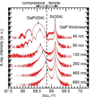
Figure 1.24 shows the ω/2θ scan profiles of specular 004 diffraction from a series of
GaP/Si layers.69 Knowing that the X-ray wavelength λ=0.1540562 nm, 2θrelaxed and
2θstrained are calculated to be respectively 68.84° and 68.61°, according to the Bragg’s Law.
The 2θ position of the fully relaxed GaP is indicated by a dashed line for easier
determination: for samples whose GaP peak is located at the left side of the line, the strain is compressive and the epilayer is strained; for those with a GaP peak at the right side of the line, the strain is tensile and there is relaxation in the layer. Notice that the peak position of the 45 nm thin layer is found to be slightly less than the theoretical fully strained position 68.61°, this disagreement may be originated form the experimental adjustement.
Figure 1.24 ω/2θ scan profiles of specular 004 diffraction from a series of GaP/Si samples.69
1.3.2
Evaluation of lattice misorientation
The heterepitaxial GaP on Si layers may consist of small “mosaic blocks” with rotational misorientation (or “tilt”) relative to one another, as shown in Figure 1.25 a). Therefore the normal directions to the crystallographic planes of same index in different
blocks are distributed within a “tilt” angle80. These blocks are much larger than the spatial
coherence length in XRD experiments (order of magnitude: 1 µm in this case) and thus
scatter X-rays incoherently with respect to each other.81,82 The reciprocal space (S//, S⊥)
being defined along the directions parallel to the layer surface and its normal, a dispersion
on S⊥ is seen within a small angle, resulting in a broadening on the diffraction peak ∆ωM,
as depicted in the Figure 1.25 b), and this broadening contribution is more evident on high
index reflections.83 Whereas the broadening due to the crystallite size (here the average
lateral size of the bloc) is constant on any reflections.
a) b)
Figure 1.25 a) Schematic presentation of mosaic structure composed of disoriented small blocs
Therefore, the tilt angle along with the average crystallite size in the direction parallel
to the layer surface can be evaluated via the decomposition of the ω scan peak broadening
of 00L reflections, that is, the Williamson-Hall method, as proposed by Williamson and
Hall in 1953. A more detailed derivation can be found in the APPENDIX of ref. 83.
1.3.3
Measurement of layer thickness
The layer thickness is another important parameter of the thin layer. The determination of layer thickness is based on the coherent interference between the layer surface and the layer/substrate interface. Considering an epitaxial layer with flat interface with good parallelism and few distortion, interference fringes can be observed in the scattering pattern. The layer thickness L can be determined using the he angular separation between the corresponding thickness fringes, which is given by the following expression, in the
case of a specular reflexion:85
∆ >K = ? LM 6 N LM6
Eq. 1–8
Differentiating P = LM6
Q , one obtains:
∆P =7RS<>T>,
Eq. 1–9
Then, combining the (
Eq. 1-8
) and (Eq. 1-9
) relationships:∆P = LM6WX 6N LM 6 =%N
Eq. 1–10
Therefore:
Z = [PK( R
Eq. 1–11
with m the fringe order and Sm its position.
Figure 1.26 shows a 004 ω/2θ scan profile of a 100-nm-thin GaPN/GaP sample86. This
is a very typical profile of heteroepitaxial layer, basically composed of a substrate peak, a layer peak and the thickness fringes. The layer thickness measured from the figure is about 114 nm, a little bigger than the nominal 100 nm.
Figure 1.26 XRD 004 ω-2θ scan profile displaying thickness fringes, the layer thickness is
measured to be 114 nm for a 100 nm-thin GaPN/GaP film.86
1.3.4
Observation of MTs in reciprocal space
All the above analyses are based on the study of the reciprocal lattice characteristics of the epilayer. Now let’s consider the MTs, being regarded as 180° rotation of the {111}-type nominal crystal planes along a [111] {111}-type axes. In reciprocal space, the twinning effect produces new reflection spots as schematically depicted in Figure 1.27. The green streaks correspond to the rotation of the nominal lattice point around the [11-1] axis, indicating the additional reflections due to the MT-A, whose boundaries are limited by (11-1) planes. The elongation of the spot along the [11-1] direction comes from the fact that the MT domain is a thin “platelet” with (11-1) boundaries. In the same way, the orange streaks correspond to the MT-C. The MT-B and the MT-D can be seen in the plane defined by the [001] and [1-10] vectors.
Figure 1.27 Reciprocal lattice points of GaP. The black, blue and red solid circles represent strong, medium and weak reflections. The green and orange ellipsoids represent respectively the MT-A and MT-C spots.
1.4
Summary
Perfect crystal doesn’t exist. Variant crystalline defects can be generated in heteroepitaxially grown thin layers, involving strain and relaxation, misfit and treading dislocations, mosac tilt, microtwins and antiphase domains. The X-ray diffraction is shown to be a powerful technique in investigating the epilayer structure. Different
techniques consisting of ω scan, ω/2θ scan, reciprocal space mapping, pole figure are
widely used in measurement of strain status, mosaic tilt angle, epilayer thickness and other structural parameters. On this basis, we are able to develop analytical methods to evaluate the structural quality of the GaP/Si layers, especially the MT and APD densities. These analyses, combined with complementary microscopic measurements, lead to a complete understanding of structural qualities of the GaP/Si layers.
Chapter 2
GaP/Si growth and characterization
techniques
This chapter presents the experimental supports of the thesis work. Firstly I will give a description on the GaP/Si samples growth, including the Si substrate, the Si surface preparation, the homoepitaxial growth of Si buffer layer and the heteroepitaxial growth of GaP layers. Then three X-ray diffraction measurement setups are presented: laboratory Bruker D8 Discover diffractometer on high resolution and low resolution mode and the beamline BM02 of European Synchrotron Radiation Facility. Finally, complementary techniques such as Atomic Force Microscopy, Transmission Electron Microscopy, Scanning Transmission Electron Microscopy and Scanning Tunneling Microscope are very simply introduced.
2.1
Growth of GaP/Si heterostructure
2.1.1
Vicinal Si substrate
The Si substrates used in this work are 2inches n-type Si(001) wafers, containing two
flats telling us the crystallographic orientation of the substrate, as shown in Figure 2.1 a). Two types of surfaces are used: the nominal Si surface with the [001] crystallographic direction parallel to the surface normal, ant the vicinal Si surface with 6 degrees miscut towards the [110] direction, as illustrated in Figure 2.1 b). The vicinal Si substrate is now widely studied since it has been shown that the APDs were formed due to polar on non-polar materials growth and could be partially avoided via double stepped Si(001) surface,
realized by the miscut of a few degrees towards the [110] direction.45,53,54
a) b)
Figure 2.1 a) Schematic representation of the Si(001) wafer orientation. b) The vicinal
substrate shows a miscut of 6° towards the [110] direction.
Indeed, on such a vicinal surface, both single-layer steps and double-layer steps can be
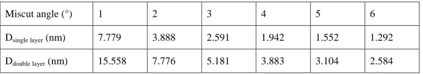
formed. The relationship between the miscut angle α, the atomic step height d and the
average terrace length D can be described as following:
tan
α
=d/D.
Eq. 2–1
Knowing that for single layers 8 = a
b and for double layers 8 = 2 ! ba, with a0 =
0.5431 nm the lattice constant of silicon in the [001] direction. Then the terrace lengths D are calculated for different miscut angles and the results are listed in Table 2.1.
Table 2.1 Calculation of the terrace lengths D for Si substrate with different miscut angles
Miscut angle (°) 1 2 3 4 5 6
Dsingle layer (nm) 7.779 3.888 2.591 1.942 1.552 1.292
According to Chadi’s notation,87 we distinct two types of steps for both single-layer (S)
and double-layer (D), labeled by SA, SB, DA and DB. The subscript denotations indicate
whether the Si-Si dimerization direction on the upper terrace near a step is perpendicular (A) or parallel (B) to the step edge, as depicted in Figure 2.2. On single stepped surface, we can observe an alternation of two domains: (1×2) for the terrace with Si-Si dimers perpendicular to the step edges and (2×1) for that with Si-Sidimers parallele to the step
edges. Therefore, the surface with with DA double steps reprenstes a single (1×2) domain
and that DB double steps represents a single (2×1) domain. The presence of single domain
is the signature of double layer formation.
a)
b) c)
Figure 2.2 Illustration of Si surface presenting a) alternation of SA and SB single steps with
(1×2) and (2×1) domains b) DA double steps with single (1×2) domain and c) DB double steps with
(2×1) single domain. The dimerization direction on the upper terrace near a step is perpendicular (for SA and DA) or parallel (for SB and DB) to the step edge,
They also calculated the formation energies per unit length λ for the four types of steps: ? Pc d 0.01 e 0.01 f /
,
? Pg d 0.15 e 0.03 f /
,
? hc d 0.54 e 0.10 f /,
? hg d 0.05 e 0.02 f /.
We have λ(DB) < ( λ(SA) + λ(SB)) < λ(DA), therefore, DB double steps with the surface
dimerization parallel to the step edge are more energetically stable, which is also
consistent with the calculation by Oshiyama88 and the experimental observations.89,90
Althouth energetically favorable, the formation of DB double steps strongly depends
on the miscut angle and the surface preparation (chemical cleaning, thermal treatement and homoepitaxial growth of Si buffer layer, etc.)
Figure 2.3 shows the evolution of double steps formation as a function of miscut
angle,91 measures under the same thermal conditions (heated for 30 sec at 1525K). The
closed squares represent the relative population of the (1×2) domain which decreases with the increase of miscut angle. The open squares represent the percentage of double steps, which increases witht the miscut angle. Both demonstrate that higher miscut angle
facilitates the formation of DB double steps.
Figure 2.3 Relative population of the (1×2) domain (closed squares, left axis) and percentage
of double steps (open squares, right axis) as a function of miscut angle. 91
Actually, the 4 degrees miscut has already been studied in our laboratory86,92 and it
turned out to be not sufficient for obtaining a perfect double stepped surface, therefore, most of the samples studied in my thesis are grown on the Si(001) substrate misoriented of 6°. The Si surface cleaning procedures have been optimized by Tra Thanh Nguyen during
his thesis (Foton, Insa Rennes)86 and will be briefly introduced in the next part. The
growth of Si buffer layer is one of the important parameters to be studied in this thesis and will be discussed in Section 4.2.2.
2.1.2
Si surface cleaning
Si is a very reactive material and contaminants such as carbon, oxide, metallic and organic impurities are easily formed on Si surface during the fabrication and storage process. Contaminants on the surface may act as a preferential nucleation site and result in
high defect density in the compound semiconductor layer93,94. Smooth and
contaminant-free Si surface is a key point to the successful epitaxial growth of III-V materials on Si to limit the defect generation. Evaluating the cleanliness of a chemical preparation is not
straightforward. Fortunately the Chemical Vapor Deposition (CVD) technique is dramatically sensitive to substrate surface contamination. Even low contaminant density results in a highly rough and pitted surface after a homoepitaxial growth. The efficiency of the silicon surface preparation can be thus investigated by post-growth surface morphology characterization of silicon buffer layers.
Firstly a cleaning process based on the standard Radio Corporation of America (RCA)
process94 and called herein the “modified RCA process” has been applied. The main steps
of the process are listed in Table 2.2.95 The sample is firstly dipped in the NH4OH-H2O2
-H2O solution for removing particles, small organic residues and most metallic impurities,
then in the HF-H2O solution and HCl-H2O2-H2O solution for oxide removal, and finally in
the HF-H2O solution after an oxidation in UV/O3 atmosphere for residual carbon removal.
These last steps are repeated 5 times.
Table 2.2 Main steps of the modified RCA process, RT means room temperature.
Chemical environment T(°C) Time (min) Effect
NH4OH : H2O2 : H2O
10: 30: 200
70 10 Particles, organic, and metals (Cu, Ag, Ni,
Co and Cd) removal; Fe and Al introduction. DI water RT 20 HF : H2O 12.5 : 237.5 RT 1 Oxide removal;
Carbon and small amount of ions (especially Cu) introduction;
Metallic residues removal; Oxide layer formation at surface. HCl : H2O2 : H2O 30 : 30 : 150 80 10 DI water RT 10 HF : H2O 12.5 : 237.5
RT 1 Oxide layer removal.
DI water RT 10
Oxydation in UV/O3 RT 2 Carbon and Sulfur removal.
DI water RT 3
HF : H2O
12.5 : 237.5
RT 1
DI water RT 3
The last 4 steps are repeated 5 times using new HF solution with the same concentration. Finally, the wafer is immersed in a new HF bath and is loaded to the reactor.