HAL Id: tel-00246549
https://tel.archives-ouvertes.fr/tel-00246549
Submitted on 7 Feb 2008HAL is a multi-disciplinary open access archive for the deposit and dissemination of sci-entific research documents, whether they are pub-lished or not. The documents may come from teaching and research institutions in France or abroad, or from public or private research centers.
L’archive ouverte pluridisciplinaire HAL, est destinée au dépôt et à la diffusion de documents scientifiques de niveau recherche, publiés ou non, émanant des établissements d’enseignement et de recherche français ou étrangers, des laboratoires publics ou privés.
on eSRAM internal signal races
Michael Yap San Min
To cite this version:
Michael Yap San Min. Statistical analysis of the impact of within die variations on eSRAM internal signal races. Micro and nanotechnologies/Microelectronics. Université Montpellier II - Sciences et Techniques du Languedoc, 2008. English. �tel-00246549�
SCIENCES ET TECHNIQUES DU LANGUEDOC
THESE
Pour obtenir le grade de
DOCTEUR DE L’UNIVERSITE MONTPELLIER II Discipline : Microélectronique
Formation Doctorale : Systèmes Automatiques et Microélectroniques Ecole Doctorale : Information, Structure et Systèmes
Présentée et soutenue publiquement par
Michael Yap San Min Le 21 Janvier 2008
Analyse statistique de l’impact des variations locales sur les courses de
signaux dans une mémoire SRAM embarquée
JURY
- Pr. Serge Pravossoudovitch , Président
- Pr. Michel Robert , Directeur de thèse
- Pr. Régis Leveugle , Rapporteur
- Dr. Jean Michel Portal , Rapporteur
- Dr. Philippe Maurine , Examinateur
- Mrs. Magali Bastian , Examinateur
I would like to thank first of all my thesis supervisor Pr Michel Robert, director of the laboratory of computer science, microelectronic and robotic of Montpellier (LIRMM), for his guidance and advice upon my arrival at the laboratory and throughout my stay at the LIRMM.
I am greatly indebted to Dr Philippe Maurine, from University of Montpellier II, and want to express my deepest gratitude for his commitment and precious technical, as well as non technical, advice he has been giving me throughout those three years of my research work. His great enthusiasm and devotion to my work have been for me a serious source of motivation in the complete realization of this work.
This thesis has been the result of an industrial collaboration between Infineon Technologies France and the ‘LIRMM’ of University of Montpellier II. I want to thank Mr Jean Christophe Vial, the manager of the memory library team (LIB MEM), for having given me the opportunity to form part of the LIB MEM team and start my PhD at Infineon Technologies.
Special thanks to Mrs Magali Bastian and Mr Jean Patrice Coste, both from Infineon Technologies (LIB MEM), for their technical expertise in embedded memories and the enlightenment they have been giving me on SRAMs.
I would also like to thank Pr Régis Leveugle from INPG, Dr Jean Michel Portal from University of Provence, Dr Christophe Chanussot from Infineon Technologies France, and Pr Serge Pravossoudovitch from University of Montpellier II for serving on my thesis committee.
I am also grateful to Mr Jean Yves Larguier, who took me as a trainee at Infineon Technologies in 2004 and gave me the chance to carry on with a PhD.
Thank you also to some designers of LIB MEM who have been providing technical advice and all the PhD students from the microelectronic department of the ‘LIRMM’ for this great working atmosphere at the laboratory.
Finally, my warm thanks to my parents, my brother and my sister for all their support, encouragement and for believing in me.
Table of contents
General Introduction 17
Chapter 1: Generalities and challenges of eSRAM 21
I.1 Classification of embedded memories 23
I.2 Challenges of SRAM memory design 25
I.3 Architecture of SRAM memories 34
I.4 Operating mode of the memory 40
I.5 Metrology of SRAM 44
Chapter 2: Variability aspects in eSRAM 50
II.1 Variability aspects 52
II.2 Failures in SRAM 68
II.3 Solutions for controlling variability in the memory 74
Chapter 3: Corner analysis and statistical method 88
III.1 The corner analysis method 89
III.2 Advantages and limitations of corner analysis method 91
III.3 Statistical modelling 92
III.4 Corner analysis and local variations 95
III.5 Modelling approach 99
Chapter 4: Applications of the modelling approach 107
IV.1 Applications 109
IV.1.1 Failure probability map 109
IV.1.2 Statistical sizing methodology of dummy bit line driver 115
IV.1.3 Dummy bit line driver with reduced variance 119
List of figures
Fig. I.0 SoC block diagram 22
Fig. I.1 Types of memories 23
Fig. I.2 Embedded memory usage 25
Fig. I.3 Total power consumption on a chip based on 2002 ITRS projection 27
Fig. I.4 Behaviour of learning curve with technology node evolution 31
Fig. I.5 Soft error failure of a chip 32
Fig. I.6 The bathtub curve 33
Fig. I.7 Block diagram of an SRAM architecture 35
Fig. I.8 Block diagram of control block 35
Fig. I.9 Block diagram of X and Y pre decoders 36
Fig. I.10 Block diagram of post decoders 36
Fig. I.11 Block diagram of memory core and 6T SRAM cells 37
Fig. I.12 Block diagram of Dummy Bit line Driver 37
Fig. I.13 Block diagram of sense amplifier and write circuitries 38
Fig. I.14 Block diagram of post multiplexer 39
Fig. I.15 Memory configurations 40
Fig. I.16 Block diagram of a read operation 41
Fig. I.17 Timing diagram of a read operation 42
Fig. I.18 Block diagram of a write operation 42
Fig. I.19 Timing diagram of a write operation 43
Fig. I.20 STG of a read operation 45
Fig. I.21 STG of a write operation 46
Fig. I.22 Definition of the read margin 46
Fig. I.23 Definition of the write margin 47
Fig. I.24 Architecture of Dummy Bit line Driver 48
Fig. II.1 Variability trend in process parameters with technology evolution 51
Fig. II.2 Classification of parameter variations 52
Fig. II.3 Within die temperature variations 53
Fig. II.4 Temperature delay sensitivity variations with respect to supply voltage
Fig. II.7 Schematic diagram for representing an aberrated lens 60
Fig. II.8 A rotatory CMP tool 60
Fig. II.9 Non uniform deposit of inter layer dielectric due to the underlying metal
pattern density 61
Fig. II.10 Parasitic charges within the oxide and at the oxide/semiconductor
interface 62
Fig. II.11 Evolution comparison between lithography wavelength and silicon
feature size 63
Fig. II.12 Data from various advanced lithography processes reported by different
labs 63
Fig. II.13 Standard deviation of VT for 2 different Leff and VT lowering with increase
of LER at drain voltage VD=1.0V (squares) and VD=0.1V (circles) 64
Fig. II.14 Correlation between VT and the concentration/semiconductor interface 65
Fig. II.15 Potential distribution at Si/SiO2 interface of a MOSFET with
(a) VT=0.78 (b) VT=0.56V 66
Fig. II.16 Halo implants at drain/source regions 67
Fig. II.17 Schematic drawing of a MOSFET with localized regions of charge due
to halo implants 67
Fig. II.18 (a) Break of 7 metal lines (b) Short of 7 metal lines 69
Fig. II.19 Reading a ‘0’ from an SRAM cell 70
Fig. II.20 Read failure of an SRAM cell 71
Fig. II.21 Writing a ‘0’ to an SRAM cell 72
Fig. II.22 Write failure of an SRAM cell 72
Fig. II.23 Leakage currents in stand by mode degrading voltage node N1 73
Fig. II.24 Latch type sense amplifier 73
Fig. II.25 Pulsed word line scheme and write and write operation timing diagram 75
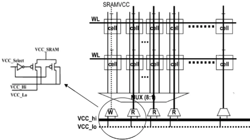
Fig. II.26 Muxing power supplies to Vcc_hi or Vcc_low based on read or write
Operation 77
Fig. II.27 Writing margin expanding scheme 78
Fig. II.28 Control circuits for sense amplifier activation 78
Fig. II.29 External test and repair 80
Fig. II.33 1Mb SRAM using word line redundancy 84
Fig. II.34 1Mb SRAM with I/O redundancy 84
Fig. II.35 Block diagram of a SEC-DED system 86
Fig. III.1 (a) I-V curve variations (b) Statistical I-V curve variations 91
Fig. III.2 Process oriented nominal IC design 94
Fig. III.3 Incorporation of SSTA tool in magma IC implementation system 95
Fig. III.4 Signal races between paths A and B 96
Fig. III.5 Notations 97
Fig. III.6 Path correlation of 1 between paths A and B 97
Fig. III.7 Pdf of path delays A and B and cdf of D for different values of
correlation coefficients 98
Fig. III.8 PV variation with respect to read timing margin for different values of ρ 100
Fig. III.9 Timing constraint violation for a delay variance of 0.05 101
Fig. III.10 Timing constraint violation for a delay variance of 0.1 101
Fig. III.11 Timing constraint violation for a delay variance of 0.03 102
Fig. III.12 Timing constraint violation for a delay variance of 0.1 103
Fig. III.13 Evolution of read timing margin with correlation coefficients for
different variance values of path B 104
Fig. III.14 Evolution of read timing margin with variability and path delay 105
Fig. IV.1 Map convention of the memory 109
Fig. IV.2 Considered scenarios for behaviour of ρ 110
Fig. IV.3 Failure probability map for (a) Uniform (b) Linear (c) Hyperbolic and (d)
Exponential variations of ρ at normal operating conditions 112
Fig. IV.4 Representation of memory areas most likely to experience read timing
constraint violations 112
Fig. IV.5 Failure probability map for (a) Uniform (b) Linear (c) Hyperbolic and (d)
Exponential variations of ρ at worst operating conditions 113
Fig. IV.6 Failure probability map for (a) Uniform (b) Linear (c) Hyperbolic and (d)
Exponential variations of ρ at best operating conditions 114
Fig. IV.7 Statistical sizing procedure of dummy bit line driver 118
Fig. IV.8 (a) Signal races between paths A and B (b) Timing diagram of read
Fig. IV.10 (a) Sensitivities of D with respect to supply voltage (b) Sensitivities of
D with respect to temperature 124
Fig. IV.11 Evolution of read timing margin at constant timing yield 131
Fig. IV.12 Reduction in read timing margin with adjustment of supply current to
supply voltage 132
Fig. IV.13 Evolution of PV with respect to temperature and voltage variations 133
Fig. IV.14 Evolution of µDcorner/µDwith respect to supply voltage variations at
List of tables
Table I.1 Low power SRAM performance comparisons 26
Table IV.1 Temperature conditions at which sizing should be performed 116
Table IV.2 Temperature at which sizing should be performed for different operating
voltages 125
Table IV.3 Correlation values of propagation delays 125
Table IV.4 Current consumption comparison of both DBDs 126
Table IV.5 Variability reductions 128
Table IV.6 Probability of a timing constraint violation 128
Table IV.7 Reduction of the read timing margin 129
Table IV.8 Reduction of the read timing margin between reference (REF) and
Proposed (Prop) DBDs with voltage adaptations 134
Introduction générale
Introduction générale
Les systèmes sur puce trouvent leurs applications dans de nouveaux appareils nomades tels que les appareils photo numériques, smart phone, PDA et autres applications mobiles. Ces systèmes sur puce se composent donc d’une multitude de blocs IP, allant des processeurs embarqués à des mémoires embarquées comme les SRAMs, en passant par des encodeurs/décodeurs MPEG et bien d’autres composants. Face à la compétition du marché dans le secteur des semi conducteurs et le temps de mise sur le marché qui reste l’une des principales préoccupations des industriels, ceux-ci font donc plus souvent appel à l’utilisation de plusieurs blocs IP, particulièrement avec l’accroissement de la complexité des puces et de leur coût. Néanmoins, les performances globales et le rendement de fabrication des circuits dépendent en grande partie des performances de ces blocs mémoires, qui peuvent représenter jusqu’à 80% de la surface totale de la puce selon l’ITRS.
Parallèlement à l’accroissement de la part dévolue à la mémoire au sein des circuits, l’évolution technologique s’accompagne d’une augmentation de la variabilité des performances, notamment dues: (a) aux variations de process (P) qui apparaissent lors des étapes de fabrication, (b) aux variations statiques et dynamiques de la tension d’alimentation (V) et (c) aux variations de température (T) dues aux variations de l’activité au sein du circuit. Ces trois paramètres constituent la définition classique de ‘PVT’.
De nombreux travaux sont actuellement dédiés à la définition de méthodes de conception statistiques permettant d’anticiper l’impact sur les performances temporelles des variations des procédés de fabrication. Ces variations des procédés de fabrication apparaissent à diverses étapes de fabrication, et constituent un sérieux obstacle lors de la phase de conception des circuits intégrés en technologique fortement submicronique.
Les auteurs de ces travaux distinguent généralement deux catégories de variations des procédés de fabrication : les variations globales et les variations locales. Une variation des procédés de fabrication (P) est dite globale si celle-ci a des conséquences identiques à l’échelle d’un circuit. Inversement, une variation est dite locale si elle ne produit des effets que sur une partie limitée du circuit, et celle-ci peut être de type systématique ou stochastique. Les variations globales (inter-fab, inter-lot, inter-wafer et inter-die) ont de nombreuses origines: planarité des wafers de silicium, aberrations optiques, hétérogénéité de la
température lors de la fabrication … De manière identique, les variations locales (intra-die) peuvent avoir différentes origines comme par exemple la variation de la concentration des dopants, la finesse de la gravure, la variation de l’épaisseur d’oxyde de grille .... Globales, ou bien locales, ces variations affectent, avec la réduction des dimensions des transistors, de plus en plus significativement les performances des circuits intégrés comme la fréquence maximale de fonctionnement, la consommation statique ou encore le rendement de fabrication. Si les variations des procédés de fabrication affectent de plus en plus les performances temporelles des circuits intégrés, la tension d’alimentation et la température demeurent des sources importantes de variations des timings et de la consommation. En effet, les fluctuations de tension sont causées par les chutes de tension RI, l’hétérogénéité spatiale et temporelle de l’activité des blocs, et la non uniformité de la distribution de la tension d’alimentation. Ces chutes de tension, bien souvent localisées, entraînent l’apparition de points chauds et l’existence de gradients de température dans les circuits qui altèrent localement les performances.
En terme de conception, ces variations de procédés de fabrication et de conditions de fonctionnement sont généralement prises en compte en adoptant une approche pire et meilleur cas. Par exemple, l’estimation à priori de la fréquence maximale de fonctionnement est réalisée en effectuant deux analyses distinctes des performances temporelles : l’une en considérant les conditions PVT les plus favorables (best case timing corner) et l’autre en considérant les plus défavorables (worst case timing corner).
Dans ce contexte, l’accroissement de la variabilité des procédés de fabrication conduit à l’accroissement relatif de la fourchette d’estimation des performances, comme la fréquence de fonctionnement d’un circuit. Ceci peut poser des problèmes de convergence du flot de conception. A titre d’exemple, dans certains cas, l’écart entre les estimations meilleur et pire cas peut atteindre 60% (en 90nm) des performances moyennes ou typiques.
Si l’accroissement du degré de pessimisme, conjugué avec à l’utilisation de méthodes pire et meilleur cas, permet de prendre en compte, lors de la conception, l’impact de la variabilité dans de nombreux cas, ce n’est toutefois pas une approche suffisante pour anticiper tous les effets liés à l’accroissement des variations intra-die ou encore à l’apparition de points chauds ou de chutes locales de la tension d’alimentation. Ainsi la seule alternative, permettant de s’affranchir des méthodes pire et meilleur cas, réside dans l’adoption de techniques statistiques et notamment l’analyse statistique des performances temporelles. Cette analyse statistique des performances des SRAMs constitue le cœur de cette thèse.
Le premier chapitre introduit les généralités et les défis des mémoires embarquées, et plus particulièrement les défis liés aux SRAMs tels que la consommation, rendement, fiabilité. Les contraintes liées à la consommation de puissance, la basse puissance et la conception en vue de la manufacturabilité vont également être détaillées. Nous présentons aussi l’architecture de la SRAM, ainsi que la complexité de ses opérations de lecture et d’écriture. Cette complexité est souvent associée aux courses de signaux qui doivent êtres parfaitement synchronisées et ce malgré les nombreuses sources d’incertitudes existantes. Cette synchronisation est réalisée par le ‘dummy bit line driver’ qui a un rôle essentiel dans une mémoire SRAM embarquée. En effet, celui-ci joue lors des cycles de lecture notamment, le rôle de métronome de la mémoire. Il garantit que les amplificateurs de lecture sont déclenchés après que la différence de potentiel entre leurs entrées ait atteint un niveau suffisant pour que la lecture se fasse correctement.
Le chapitre deux fait un état de l’art des sources de variations de la mémoire causées par des dérives des procédés de fabrication (local ou global), des conditions environnementales (tension d’alimentation, température) et des conditions de vieillissement (NBTI, claquage d’oxyde de grille). L’impact de ces phénomènes de variabilité sur la performance de la SRAM y est analysé, en terme de défaillances paramétriques sur les performances du point mémoire et les divers blocs fonctionnels de la mémoire SRAM. De plus, les techniques les plus courantes pour palier à ces problèmes sont présentées. Parmi les méthodes présentées qui prennent en compte ces variations, nous retrouvons les techniques de pulse et la variation de la tension d’alimentation utilisées pour la conception du point mémoire en présence de la variabilité. Des méthodes telles que la redondance (de ligne, de colonne…) et les codes correcteurs d’erreurs y sont aussi introduits.
Dans le troisième chapitre, nous débutons par l’introduction de la méthode traditionnelle (méthode de corner) très couramment utilisée et qui est basée sur la détermination des conditions extrêmes de fonctionnement d’un circuit : l’une en considérant les conditions PVT
les plus favorable et l’autre en considérant les plus défavorables. Nous démontrons les
limitations de l’analyse de corner et de son incapacité à considérer les variations locales. Nous montrons que l’accroissement progressif des variations locales peut conduire des analyses de corner, effectuées sur des courses de signaux, à être optimistes, d’où la nécessité de développer des techniques de conception statistique. Afin de faire face à l’optimisme et au pessimisme de l’analyse de corner, nous proposons une modélisation permettant d’évaluer la marge temporelle de lecture requise sans être trop optimiste ou pessimiste dans notre
estimation, et permettant également d’évaluer la probabilité de satisfaire cette contrainte temporelle. Cette modélisation permet donc de prendre en des variations locales dans le calcul des marges temporelles de lecture dans la mémoire.
Les applications de la modélisation introduite au chapitre trois sont présentées dans le chapitre quatre. Les deux applications comprennent : (i) la définition à priori de cartographies du plan mémoire de probabilité d’occurrence de violations des contraintes temporelles, (ii) la mise au point d’une méthode de dimensionnement statistique d’un bloc particulier de la mémoire, appelé ‘dummy bit line driver’. Cette structure est un élément essentiel des mémoires SRAMs auto synchronisées. Le ‘dummy bit line driver’, en l’absence de signal d’horloge interne à la SRAM, joue en effet le rôle de métronome en indiquant à l’amplificateur de lecture quand lire la donnée. Nous introduisons un nouveau ‘dummy bit line driver’ présentant une sensibilité réduite aux variations de procédés et des sensibilités à la tension d’alimentation. L’utilisation conjointe de la méthode de dimensionnement statistique et du ‘dummy bit line driver’ permettent de réduire significativement la variabilité des délais des chemins et les marges de conception, tout en garantissant un rendement temporel donné.
General Introduction
General introduction
System on Chip devices, have found their applications in every latest hand-held consumer devices, like smart phones, PDAs, digital cameras and other mobile applications. These SoCs embrace a variety of IP cores, such as embedded processors, MPEG encoders/decoders, DSPs, embedded memories which include SRAMs and more. As time to market has become the main obsession for every company wanting to remain very competitive on the market, the semiconductor companies need to license more and more IPs, particularly with an increase in the complexity of the chip and soaring design costs. However, the global performances and the fabrication yield of the chips are governed in majority by memory blocks, which account for a large percentage of the surface of the chip (around 80% according to the ITRS).
Simultaneously with the rapid increase in memory blocks within the chips, technology evolution is accompanied by an increase in performance variability owing to: (a) process variations (P) which appear due to manufacturing phenomena, (b) static and dynamic variations of the supply voltage (V) and (c) temperature (T) fluctuations due to varying activity levels within the circuit. Those three parameters constitute the classic ‘PVT’ definitions.
Currently, statistical design methods have been the focus of substantial research in order to anticipate the impact of manufacturing process variations on timing performances. These process variations appear at different levels during the manufacturing steps and have emerged as a serious bottleneck for the proper design of ICs in the sub nanometre regime. They are generally classified into two distinct groups of manufacturing processes, namely global and local variations. Global variations, caused by inter-fab, inter-lot, inter-wafer and inter-die processing variations, originate from several factors which include non uniform chemical polishing (CMP) which occurs due to different pattern densities, lens aberrations, non uniformity of the temperature and more. Global variations are said to affect every element on the chip equally or in a systematic way. On the other hand, local variations or currently known as mismatch result from random dopant fluctuations, line edge roughness, surface state charge, gate depletion and film thickness variation. Local variations are characterized by differences between supposedly identical structures found on the same die, but these variations display either a systematic or a random behaviour. In fact, transistor scaling has
exacerbated the impact of local and global variations, affecting performances of integrated circuits, for instance their maximum operation frequencies and static power consumptions or even the manufacturing yields.
Although manufacturing process variations influence more and more the timing performances of ICs, supply voltage and temperature fluctuations also constitute important sources of timing variations. Indeed, voltage variations are due to IR drop, switching activity of different areas of the chip and non uniform power supply distribution, whereas temperature variations stem from the existence of temperature gradient due to different switching activities in the chip. This condition gives rise to the appearance of hot spots. These hot spots cause important differences in temperature between different areas of the die.
To handle the impact of manufacturing process variations along with the operating conditions in circuit design, corner based methodology is performed by characterizing the circuit under best case and worst case conditions. For instance, the estimation of the maximum operating frequency is carried out at least under 2 distinct timing analysis conditions: one while considering the best PVT conditions (best case timing corner) and the other one by considering the most unfavourable conditions (worst case timing corner).
In this context, the increase of variability in manufacturing processes results in an underestimation of performances in the operating frequency of an integrated circuit. This can therefore impact on the convergence of the design flow. In certain cases, the differences in the estimation between best and worst cases can reach 60% of the mean performances.
If the increase of optimism and pessimism, introduced by best and worst cases, takes into account the effect linked to variability in circuit design under certain classic aspects, this approach is insufficient in foreseeing all the impacts due to an increase of intra-die variations or even with the appearance of hot spots or local IR drop of the power supply.
Thus, statistical analysis method is emerging as the solution to account for these sources of variations, and provides more accurate analysis results of the circuit in terms of timing analysis.
The first chapter introduces the generalities and the challenges of embedded SRAMs. In this chapter, challenges dealing with power consumption, low power and design for manufacturability issues are being discussed. A detailed explanation of the architecture of the SRAM is also provided, describing the functionalities of each of its blocks. We also highlight the complexities of SRAM operations, involved in read and write operations, due to signal
races in the memory. In fact, the memory needs to be perfectly synchronized in the presence of those variability conditions.
Chapter two presents the variability aspects encountered by the memory. The major sources of variations owing to manufacturing processes, environmental conditions and aging conditions are introduced herein. We explain the impact of these sources of variations on the memory performances and give some of the most common techniques, related to the memory cells and to the memory architecture, used to mitigate the effects of variability.
In chapter three, we demonstrate the limitations of the corner analysis method and its inability in capturing local variations. We illustrate that an increase in local variations leads to optimistic conclusions when corner analysis is undertaken during racing conditions in the memory, and the need for developing statistical design techniques. More precisely, to overcome the optimism and the pessimism caused by corner analysis, we provide a simple modelling approach for computing the appropriate read timing margin in the memory and the probability of fulfilling this timing constraint.
Chapter four displays some applications of the modelling approach introduced in the previous chapter. The two applications include: (i) displaying a failure probability map of the memory core which shows its most critical areas that are more likely to meet timing constraint violations during a read operation, (ii) developing a statistical sizing methodology of a particular block of the memory, dubbed dummy bit line driver. This structure plays an important role in an auto synchronized memory during the read operation, since it is responsible in triggering the sense amplifier at the appropriate time when a memory cell is being read. We also introduce a new dummy bit line driver having its timing performances more robust to process and voltage variations. The use of the statistical sizing methodology developed and the proposed dummy bit line driver demonstrate better performances in terms of the reductions in path delay variabilities and read timing margins, compared to the original dummy bit line driver.
Chapter 1
_____________________________________
Generalities and challenges of eSRAM
Embedded memories have become increasingly important as they form the major component of SoCs. This chapter focuses on the generalities of SRAMs, their functionalities and the associated complexities involved in SRAM’s operations. These complexities arise due to the presence of racing signals, which need to be correctly synchronized in the presence of variability phenomena. We also introduce herein some of the main challenges i.e. yield and reliability issues faced by SRAMs as the transistor is continuing to shrink relentlessly.
INTRODUCTION
The advent of system on chip devices has paved the way to its widespread applications in a myriad of domains, ranging from the automotive sectors to the communication industries, which include numerous latest hand-held consumer devices like smart phones, PDAs, digital cameras and other mobile applications. However, system on chip technology is setting designers the very challenging problem of adopting new techniques to get the SoC operating properly the first time in several embedded applications and in a minimum time to market, through shorter design cycles. This is mainly due to today’s rapidly growing number of gates per chip reaching several millions, according to Moore’s law which states that “the number transistors on a chip doubles about every two years”. To bridge the gap between this fast technology’s evolution and the lack of available manpower, designers make use of predefined modules to avoid reinventing the wheel with every new product. These blocks known as intellectual property cores (IP) or Virtual Components (VC), usually come from third parties or are sometimes designed in-house. Among the different existing IP blocks, these include DSPs, microprocessors, mixed signal blocks (ADC, DAC) and embedded memories as shown in figure I.0 below.
Fig. I.0 SoC block diagram
This chapter focuses on the generalities and challenges of eSRAMs. The first part describes existing types of memories. Next, the different challenges experienced by SRAM will be analysed, followed by a description of its architecture so as to understand its operating mode. Then, in the last section, we will see the complexity involved in the read and write operations
due to signal races and how this condition is being handled, through the introduction of a dummy bit line driver structure.
I.1 Classification of embedded memories
Embedded memories can be categorized as volatile and non volatile memories. This is illustrated figure I.1 that gives evidence of the large choice of memories available.
Memories SRAM DRAM RAM Volatile FERAM
RAM Re-writable ROM
Non Re-writable ROM
Non Volatile
MRAM PCRAM PROM EPROM EEPROM FLASH Mask ROM
Memories SRAM DRAM RAM Volatile FERAM
RAM Re-writable ROM
Non Re-writable ROM
Non Volatile
MRAM PCRAM PROM EPROM EEPROM FLASH Mask ROM
Fig. I.1 Types of memories
I.1.a Volatile Memory (VM)
The volatile memory, as it name implies, loses data when the supply voltage is switched off. It consists only of Random Access Memory (RAM) which can further be split into Dynamic RAM (DRAM) and Static RAM (SRAM). Both DRAM and SRAM allow read and write operations of the cell in the memory chip.
DRAM memory has the advantage of being cheaper and smaller in size than SRAM memory (1T cell instead of 6T for SRAM), offering a higher density. However, this higher density comes with a slower read/write operation owing to a capacitor which needs to be discharged/charged during these operations.
This does not constitute the only drawback of DRAM over SRAM. Indeed, due to leakage currents, the capacitor associated with a DRAM cell needs to be regularly refreshed to avoid loss of stored data. The refreshed logic needed therefore makes DRAM a more complex technology compared to SRAM. As a result, SRAM memory has the advantages of featuring
higher speed than DRAM (6T) and requires no refreshing operation; nonetheless it has a higher cost than DRAM.
I.1.b Non Volatile Memory (NVM)
Non volatile memories can be classified into three distinct categories:
(i) Non Volatile RAM
(ii) Re-writable ROM
(iii)Non re-writable ROM.
Examples of non volatile RAM include:
(i) Ferroelectric RAM (FeRAM) which uses a ferroelectric layer and possesses a
similar architecture to DRAM,
(ii) Magnetic RAM (MRAM) which is composed of ferromagnetic materials for storing
data
(iii)Phase Change RAM (PCRAM) making use of chalcogenide alloys for switching
between crystallized and amorphous states. The PCRAM operation is based on the different resistively of the materials for storing data.
Re-writable ROM includes:
(i) Programmable ROM (PROM) which is a one time programmable memory
performed by burning fuses in an irreversible process,
(ii) Erasable Programmable ROM (EPROM) which is programmed electrically and
data are erased from the memory cells by using ultraviolet illumination,
(iii)Electrically Erasable PROM (EEPROM) in which the programmed and erased
operations are both done electrically
(iv) Flash memory which stores data in a floating gate and is programmed and erased
electrically.
Non re-writable ROM, only meant for read operation, consists for its part of Mask ROM in which data are written after the chip fabrication by the IC manufacturer. This is done by making use of a photo mask.
I.2 Challenges of SRAM memory design
In this part, we will detail the specific challenges encountered by circuit designers in designing the memory. Examples of theses challenges include power consumption, low power issues and Design for Manufacturability (DFM) aspects.
I.2.1 SRAM performances in 90nm and 65nm nodes
SRAM memories have become a critical component of SoC devices since they occupy around 80% of chip’s surface as shown in figure I.2 below [Zor02]. Hence, the performance of the SoC depends a lot on the performances of these memories, which are meant to operate at low voltage, consume less power and achieve higher manufacturing yield.
Fig. I.2 Embedded memory usage
In these recent years, the extensive use of low voltage SRAMs in mobile applications has also been driven by the necessity for faster operating and less power consuming memories. Table I.1 below represents different sizes of SRAMs and their respective performance comparisons in 90nm and 65nm technology nodes. In the 65nm node, the memories operate at a higher frequency (around 1.5 times faster than in 90nm node) while their dynamic powers are roughly the same as 90nm SRAM memories. As far as static power is concerned, the power reduction achieved in 65nm process lies between 2 to 6 times compared to the power consumed in a 90nm process. This reduction in static power consumption is achieved by using MOS devices in the input/output (IO) blocks having threshold voltages which have been increased by 25% in the 65nm compared to the 90nm node. As for transistors in the
SRAM cells in 65nm technology, they possess threshold voltages showing up to a 37% increase compared to those of the 90nm process.
Table I.1 Low power SRAM performance comparisons
Frequency (Mhz) Dynamic Power (mw) Static Power (µw) Memory Size Power Supply (Vdd) 90nm Process 65nm Process 90nm Process 65nm Process 90nm Process 65nm Process 128b 1.0 617 666 2.4 2.0 1.2 0.2 128b 1.2 990 1087 5.5 5.0 2.2 0.4 128b 1.32 1136 1315 8.3 7.6 3.3 1.2 64kb 1.0 249 308 3.9 3.2 11.0 2.9 64kb 1.2 431 625 8.7 8.9 22.7 6.2 64kb 1.32 487 719 12.1 12.6 35.0 10.5 128kb 1.0 248 305 6.6 5.0 12.2 3.3 128kb 1.2 431 617 14.3 14.8 24.9 7.1 128kb 1.32 485 709 19.8 20.7 38.3 12.4 256kb 1.0 248 301 11.9 9.1 14.7 4.0 256kb 1.2 427 598 25.1 25.7 29.4 8.9 256kb 1.32 483 689 35.0 35.7 44.9 16.3
I.2.2 Power consumption
Power consumption is an important issue in the design flow of memories, especially in very deep submicron technologies, and this phenomenon will be exacerbated as technology continues in scaling down. This is mainly true as transistor densities increase, leading to an increase in the complexity of the chip, which further needs to operate at a higher frequency. These factors have brought forward the total power dissipation problems in the memory. The total power consumed can be defined as the sum of dynamic and static power dissipated in the memory. Dynamic power refers to the total power consumed by the memory during a read or write operation involving the switching of the logic states in the various memory blocks, and the short circuit power resulting from a current flow between supply voltage and the ground.
P
Dyn=
⋅
C
out⋅
V
dd⋅
F
+
I
SC⋅
V
dd 2where η is the activity rate, Cout the output load capacitance, F the operation frequency of the
memory, Vdd the supply voltage and ISC is the short circuit current.
On the other hand, static power of the memory is the power consumed when the memory is either in the standby mode or when the power is off. As a result of the memory’s state, the resulting leakage currents including [Roy03] reverse biased diode leakage, subthreshold current, gate leakage, Gate induced Drain Leakage current (GIDL) and the punch through current dissipate power.
dd leak
Stat I V
P ==== ⋅⋅⋅⋅ (I.2)
where Ileak represents the sum of all the leakage components.
The reverse biased diode leakage is due to the drain/source reverse biased conditions, causing pn junctions leakage current. Subthreshold current results from a current flow between the drain and source of the transistor when gate voltage is below the subthreshold voltage. Gate leakage corresponds to the tunnelling of a current from substrate to the gate and vice versa owing to a decrease in the gate oxide thickness and an increase of an electric field across the oxide. The GIDL current is due to the depletion at the drain surface below the gate/drain overlap region, leading to a current flow between that region to the substrate. The punch through current comes from the merging of the depletion region between the drain and source which gives rise to a current between these two regions. As an illustration, figure I.3 features the evolution of the two main leakage current components with the scaling of technology [kim03].
This figure highlights the 2002 ITRS projected exponential increase of the subthreshold and gate leakage as the gate length decreases. The normalized chip power dissipation corresponds to 2002 ITRS projection normalized to that of 2001. It can be seen that an alternative to control gate leakage as gate oxide thickness reduces is to make use of high K dielectric materials, which can bring gate leakage under control. In [Bor05], the author explains that replacing the gate oxide with a high K material showing the same capacitance as the silicon dioxide but with higher thickness will minimize gate leakage. Nevertheless, the same problem will be encountered as the dielectric thickness will scale down over time.
Circuits showing excessive power dissipation characteristics are more prone to run time failures and present reliability problems. Every 10˚C increase in operating temperature approximately doubles a component’s failure rate, thereby increasing the need of expensive packaging and cooling strategies [Mar99]. So as to minimize static and dynamic power dissipations, several low power techniques have been widely used as detailed in the next part.
I.2.3 Low power
Low power SRAM circuit has become a major field of interest, especially in the reduction of power consumption. Several low power techniques so far have enabled the proper operation of memories, though their complexities have kept on increasing to satisfy the high speed demand and throughput computations in various battery-backed applications. Some of the most widely used techniques in reducing power consumption include reduction of capacitance associated to bit lines and word lines through multi banking [Mar99], controlling the internal self-timed delay of the memory to track properly the delay of bit lines across operating conditions [Amr98], Dual Threshold design (DTCMOS) [Roy03] and the sleep mode concept [Ito01].
The largest capacitive elements in the memory are the word lines and bit lines each with a number of cells connected to them. Thus, reduction of the capacitive elements associated to these lines can reduce dynamic power consumption. This is achieved by partitioning the memory into smaller subarrays, such that a global word line is divided into a number of sub word lines. Similarly in multi banking, bit line capacitive switching is reduced when memory is being accessed as those bit lines are always involved in a discharge and precharge process.
Another dynamic power reduction technique consists in using a replica technique for word line and sense control in the SRAM. If this technique mainly aims at sequencing the read operation, it is also extremely efficient for low power design since it eases the use of static or dynamic supply voltage scaling techniques. In read operation, the technique consists in tuning properly the self timing circuitry by using a dummy driver and dummy core cells in order to trigger the sense amplifier when a desired differential voltage has accumulated on the pair of bit lines considered. In doing so, a fast sensing of the minimum differential voltage is performed.
Dual threshold design (DTCMOS design) is also a good approach to reduce the leakage in SRAM memories. Indeed, making use of high and low threshold voltage transistors along uncritical and critical paths allow significant reductions of the overall leakage. This technique is almost interesting as it is fully compliant with the application of the sleep mode concept. The latter implies powering down the periphery logic while the voltage level of the SRAM arrays remain activated for data retention purpose. However, this method is only useful if the memory remains idle for a long period.
Some of the above stated techniques can lower both static and dynamic power but the best mix depends on which types of power dissipation problems a designer wants to minimize and the technology in which the design is being performed.
I.2.4 Design for Manufacturability (DFM)
As the complexity in the density of transistors is skyrocketing along with shrinking of transistors, devices in embedded memories are becoming more sensitive to the disturbances of IC manufacturing processes. Due to this inherent problem, traditional CAD tools which were meant to simplify the work of designers by allowing them to create the nominal design meeting the desired performance specifications are no longer satisfactory [Zha95].
Furthermore, environmental conditions such as temperature fluctuations and voltage variations also induce IC performance variations to increase. The variability effects may for example cause faulty read or write operations in an SRAM due to an increase in access time. To cope with this problem and avoid unnecessary yield losses, designers had to revamp the IC design methodologies and introduce new design techniques.
For instance, statistical techniques can take into account the variability effects which are the root causes of parametric and functional failures in chips. Subsequently, design for manufacturability issue is gaining momentum at each stage of the design procedure in view of improving the yield and reliability of ICs, thereby ensuring stable volume production. The next two sub sections introduce the two main facts related to DFM, yield and reliability challenges.
I.2.4.1 Yield Challenge
I.2.4.1.1 Yield learning during ramp up phase
The improvement of production and cost effectiveness in the semiconductor industry have become an increasing necessity in this very competitive sector, owing to pressure arising from shorter time to market and time to volume (TTV). The period elapsing between the completion of development of the product and its full capacity production is referred as production ramp up [Ter01]. C. Terwiesch and R. E. Bohn [Ter01] specify that two conflicting factors characterize this period, a low production capacity (poor yield) and a high demand due to the “relative freshness” of the product. The pressure faced by the industry between low capacity and high demand is referred to as the “nutcracker”. In fact, very often it takes a longer time to achieve a higher yield during ramp up as technology node shrinks. This is illustrated in figure I.4 which represents the cycles of learning for three different technology nodes and their respective empirical yields. For instance, in order to achieve a yield of 90%, the number of yield cycles learning required doubles as the process technology moves on from 130nm to 65nm. This increase in learning is attributed to yield detracting mechanism which occurs more frequently as devices shrink and become more sensitive to variability aspects.
P. K. Nag and W. Maly [Nag93] defined the cycles of learning or improvement as the total time needed to:
(i) detect and localize a failure, which leads to process intervention (Tf)
(ii) process the correction and for new parameters to become effective (Te)
(iii) and the time between performing process correction and the time when yield improvement is realized (Tr).
r e f
C
T
T
T
T
=
+
+
(I.3)Fig. I.4 Behaviour of learning curve with technology node evolution.
I.2.4.1.2 Yield enhancement during production phase
During the production phase, memory yield is defined as the percentage of fully functional memory chips from all of the fabricated chips or, alternatively by the ratio between the fully functional memory chips and all the fabricated chips [Har01].
However, the large scale integration of memory area on a SoC not only leads to an increase in the size of the die but it can be problematic for the SoC’s yield due to its great dependency on the yield of the embedded memory, since the area memory covers around 80% of the total surface of the chip according to figure I.2.
In fact, memory yield is limited by numerous manufacturing defects which stem from process disturbances or non optimal design due to aggressive scaling of transistors. These may cause either inadequate performance for example excessive power consumption, too long delay giving rise to timing constraint violation, or functional failure due to spot defects which produces shorts or opens in the circuit’s connectivity [Mal96].
Hence to achieve lower silicon cost i.e. to make multi million transistor systems on a single die both feasible and cost effective, there is an urgent need for providing effective methods to improve memory yield.
In addition to stringent fabrication control (intentional process de-centering) and statistical worst case design, this can be achieved though the use of redundancy [Har01, Kim98, Zor02] added to the circuits, which consists in replacing defective circuitry with spare elements.
Some of the different types of redundancies include word redundancy, wordline redundancy, bit line redundancy and IO redundancy [Rod02]. Word redundancy consists in adding a few redundant flip flop based words, each of which corresponds to a logical address of the RAM. In word line redundancy approach, it is possible to replace one or more word lines with spare rows. Bit line redundancy for its part involves adding redundant column to the memory array whereas IO redundancy consists in replacing the bit lines along with their respective sense amplifiers with redundant elements. In addition to redundancy, error detector and correcting code can also be used to improve the yield. Yield improvement method will be discussed in further details in the next chapter.
I.2.4.2
Reliability issue
Reliability issue is emerging as a design challenge in embedded memories, especially as transistors geometry shrink, thus making SRAM more prone to soft errors. These soft errors are caused by neutrons from cosmic rays or α-particles from radioactive impurities in electronic material that may cause new data to be written in the memory. Figure I.5 [Bor05] shows the random errors occurring in a chip (logic and memory).
Fig. I.5 Soft error failure of a chip
According to [Bor05], the expected rate of increase of the relative failure per logic state bit per technology node will be around 8%. Moreover in the 16nm generation, the failure rate will be almost 100 times that at 180nm.
In addition to soft errors, physical breakdown and other degradation mechanisms like gate oxide breakdown in NMOS and the Negative Bias Temperature Instability (NBTI) effect
[Mcp06] in PMOS also affect SRAM reliability. For instance, NBTI phenomenon impacts on the read stability of the memory. Commonly, memory reliability is expressed by the probability that the memory performs its designed functions with the designed performance characteristics under the specified power supply, timing, input, output and environmental conditions until a stated time t [Har01].
Reliability specialists often represent the failure rate of a memory (Mean Time to Failure or MTTF) with the time of device usage t by the traditional bathtub curve indicated in figure I.6 below. The bathtub curve possesses three distinct periods i.e. a decreasing failure rate representing the infant mortality period, followed by a constant failure rate which is characterized by a useful device life and terminates by an increasing failure rate due to a wear out period.
Infant mortality problems have been for long a critical issue to both manufacturers as well as to customers receiving memory products lasting for a few hours to few months. These defects arise from left over or latent defects that do not necessarily expose themselves and can skip manufacturing tests [Mak07]. They manifest themselves through intensive electrical and thermal stresses during use, causing a significant functionality problem.
Useful life
Infant mortality
Wear-out
Time
F
a
ilu
re
R
a
te
Fig. I.6 The bathtub curve
To counteract infant mortality problems and improve product robustness, several techniques are widely used, for instance the burn-in test. In this process, extreme operating conditions i.e. high temperatures (up to 150˚C) and high operating voltages are applied for example at the wafer level to stress the device and accelerate the memory’s failures within some hours. Consequently, failing memory chips can be discarded.
The useful life period corresponds to the time lapse whereby memory products have the lowest failure rate. In other words, it represents the useful device period of the product which has entered a normal life. The wear-out phase occurs after the useful life period as the product ages, resulting in an increasing failure rate. Wear out phase results from electromigration problems (accelerated by high temperature and operating frequency conditions) and oxide break down triggered by high electric field conditions with decrease in gate oxide thickness. The reliability aspect is undoubtedly closely related to yield performance, since a high reliability is translated onto very high yield related constraints, both in functionality and correct parametric features [Pap07].
I.3 Architecture of SRAM memories
Figure I.7 shows the block diagram of a synchronous single port SRAM. It is composed of:
(i) Memory cores (left and right) containing a matrix of 6T SRAM cells. Each memory cell
is connected to a pair of bit lines (BL/BLB) and either BL or BLB is discharged when a row of cells is selected through word line.
(ii) A timing generator block providing the internal signals for activating an operation.
(iii)X and Y decoders to access the required cell as the input addresses are specified.
(iv) A dummy bit line driver, an important block for synchronizing the internal signals in a self-timed memory.
(v) An I/O circuit consisting of :
a. column multiplexer found in the Y post decoder
b. sense amplifiers and write circuitry
c. output buffers found in the post multiplexer
The architecture of the SRAM shown in figure I.7 is referred to as a butterfly memory. It is so called owing to its symmetry with a left and a right memory core. The next sub section details the functionalities of each block.
X post decoders
Dummy Bit line Driver (DBD)
Left memory core Right memory core
X pre decoders
Y pre decoders
Y postdecoders Y post decoders
Sense amplifiers and Write circuitries
Sense amplifiers and Write circuitries Post multiplexers Timing generator core cell Word line Bit line
Data in/Data out Control signals Clock Input address BL BLB Post multiplexers BL BLB S SB PG PD WL PU 4
Fig. I.7 Block diagram of an SRAM architecture
I.3.1 Functional blocks of the SRAM architecture
I.3.1.1 Control Block
Timing generator RWB SLOWB CLOCK WLEN BLEN IRWB IREN WLSDUM SLOWB BLDUM from DBD RWB_BUF CSB SLEEPB RSTB Timing generator RWB SLOWB CLOCK WLEN BLEN IRWB IREN WLSDUM SLOWB BLDUM from DBD RWB_BUF CSB SLEEPB RSTB
Fig. I.8 Block diagram of control block
The timing generator or control block, as shown in figure I.8, receives the input signals (control signals and clock) and generates the appropriate signals for either triggering a read or write operation or setting the memory in a sleep mode operation. The control signals are composed of 4 signals:
(i) a read/write input signal (RWB) which is low in the write mode and high for a read mode,
(iii)a slow mode signal (SLOWB) specifying whether the memory is operating in a high performance mode (SLOWB high) under high operating voltages or low performance mode (SLOWB is low) in ultra low power operating conditions,
(iv) and an active sleep mode input signal (SLEEPB) for leakage reduction in standby mode.
I.3.1.2 Pre Decoder
X pre decoder WLEN X0 . . X8 WLSA Y pre decoder BLEN BLS0 Y0 Y1 BLS1 BLS2 BLS3 Y pre decoder msb BLS4 Y2 Y3 BLS5 BLS6 BLS7 BLEN WLSB WLSC X pre decoder WLEN X0 . . X8 WLSA Y pre decoder BLEN BLS0 Y0 Y1 BLS1 BLS2 BLS3 Y pre decoder msb BLS4 Y2 Y3 BLS5 BLS6 BLS7 BLEN WLSB WLSC
Fig. I.9 Block diagram of X and Y pre decoders
The pre decoder can be either in X or Y depending upon their functionalities. In fact, the X pre decoder receives input X addresses (X0 to X8) and selects the appropriate row decoder among several row decoders in the X post decoder, via signals WLS (A/B/C) (figure I.9) Similarly, the Y pre decoder is meant for receiving input Y addresses (Y0 and Y1) and BLEN after which, the required column multiplexer among several multiplexers is chosen in the Y post decoder by the signals BLSi (i=0 to 3). As for the Y pre decoder msb block, the latter receives input addresses Y2 and Y3 and signal BLEN and produces signals BLSn (n=4 to 7). BLSn signals will be used in the post multiplexer block for selecting the read or write circuitry.
I.3.1.3 Post Decoder
X post decoder WLSA WL RSTB WLSB WLSC Y post decoder BLS0 . . . . BL SA W BLB BLS3 SAB WB X post decoder WLSA WL RSTB WLSB WLSC Y post decoder BLS0 . . . . BL SA W BLB BLS3 SAB WB
Fig. I.10 Block diagram of post decoders
The X post decoder and Y post decoder receive their respective input signals WLS (A/B/C) and BLSi (i=0 to 3) from the X and Y pre decoders (figure I.10). The X post decoder or more commonly known as row decoder generates the signal word line WL and picks out the
appropriate row of SRAM cells amid several rows, corresponding to the row where a datum is supposed to be read from or written to. The signal RSTB resets WL to 0 after the operation. For its part, the Y post decoder which is composed of a series of column multiplexers selects the corresponding column of SRAM cells (BL/BLB) through 1 multiplexer, after receiving the signals BLSi issued from the Y pre decoder. Its output signals SA/SAB and W/WB are connected respectively to the sense amplifier and the write circuitry block.
I.3.1.4 Memory Core
WL0 . . BL BLB WLn . . . . BL BLB S SB PG PD WL PU . . . cc cc cc cc WL0 . . BL BLB WLn . . . . BL BLB S SB PG PD WL PU . . . cc cc cc cc
Fig. I.11 Block diagram of memory core and the 6T SRAM cell
The memory core, left or right, is comprised of the elementary SRAM cells or core cells (cc) where data (‘0’ or ‘1’) are stored at nodes S and SB (figure I.11). A 6T SRAM cell is composed of two inverters formed by four transistors (two pull up PMOS transistors PU and two pull down NMOS transistors PD) and two pass gate transistors PG connected to a pair of bit lines (BL and BLB). The flip flop operation is achieved by connecting the input and output of one inverter to the output and input of the other inverter.
I.3.1.5 Dummy Bit line driver
Dummy Bit line Driver
WLSDUM
BLDUM
RWB_BUF Iadj1 ……. Iadjn
Dummy Bit line Driver
WLSDUM
BLDUM
RWB_BUF Iadj1 ……. Iadjn
Fig. I.12 Block diagram of Dummy Bit line Driver
Figure I.12 represents the block diagram of the dummy bit line driver (DBD), which is one of the most essential components of the memory. It consists of a series of parallel branches of stacked transistors, with the stacked transistors representing the pass gate and pull down
transistors (figure I.12). The DBD receives WLSDUM and RWB_BUF signals from the control block. RWB_BUF signal sets the use of the DBD in either a read (RWB_BUF=1) or write mode (RWB_BUF=0), input pins Iadji (i=1 to n) control the discharge rate of BLDUM and hence the memory is set either in a fast or slow read mode or write mode. On the other hand, WLSDUM activates or deactivates the transistors PGi (figure I.24) representing the pass gates of the SRAM cell. It should be noted that pins Iadji are either hardcoded or provided by the environment. The most important role of the dummy bit line driver is displayed during the read and write operation. In fact, it is the dummy bit line driver which fires the sense amplifier, through the control block, at the right time when a datum is read from a selected SRAM cell. As for the write operation, the dummy bit line driver ensures that sufficient time is given to a datum to be properly written in the SRAM cell before switching off the word line.
I.3.1.6 Sense amplifiers and Write circuitries
Sense Amplifiers and Write circuitries IREN IRWB SA SEL_R SEL_W SAB W WB Z DIN Sense Amplifiers and
Write circuitries IREN IRWB SA SEL_R SEL_W SAB W WB Z DIN
Fig. I.13 Block diagram of sense amplifiers and write circuitries
In figure I.13, signal SEL_R (from post multiplexer block) is used for selecting a sense amplifier corresponding to the column of core cells which has been chosen. The output signals SA/SAB from the multiplexer block correspond to the input signals of a sense amplifier. The sense amplifier consists of a cross coupled latched amplifier connected to a pair of bit lines. It senses the difference in potential between BL (SA) and BLB (SAB) associated with the SRAM cell, when BL or BLB is being discharged by the core cell during a read process. Once the difference in voltage between BL and BLB reaches an appropriate level (around 10% of VDD), the sense amplifier is triggered by signal IREN and amplifies the differential voltage. The output value is collected as Z. Similarly, SEL_W (from post multiplexer block) is involved in the selection process of a write circuitry attached to the column of SRAM cells where a ‘0’ or ‘1’ needs to be written at a predefined memory cell
address. The datum DIN is transmitted to the SRAM cell as output signals W (BL) and WB (BLB) when signal IRWB is turned on.
I.3.1.7 Post Multiplexer
Post multiplexers SEL_W SEL_R Z BLS4 . . BLS7 DIN DOUT DIN Post multiplexers SEL_W SEL_R Z BLS4 . . BLS7 DIN DOUT DIN
Fig. I.14 Block diagram of post multiplexer
The post multiplexer is the block through which data transit during a read or write operation (figure I.14). It consists of several multiplexers and a latched structure for storing the data read (Z), before being transmitted to the output pin as DOUT. It is also composed of buffers for transmitting input data DIN to a specified address in the memory core during a write operation. Moreover, the post multiplexer produces signals SEL_R and SEL_W from its input signals BLSi (i=4, 5, 6, 7), issued from the Y predec_msb block so as to choose the needed sense amplifier or writing circuitry.
I.3.2 Configurations of the Memory
The memory, with butterfly architecture, shows three available configurations i.e. tall, normal and wide depending on the type of multiplexers used in the post multiplexer block (figure I.15). For instance, a tall configuration uses a 4:1 multiplexer, a normal configuration uses an 8:1 multiplexer and a wide configuration uses a 16:1 multiplexer.
Hence, the choice of the type of column multiplexer influences the size of the memory. To have a better understanding, let us first start by defining the word width (WW) as the number of bits per word and the word depth (WD) as the number of words. The word width varies from a miminum of 4 bits to 128 bits with increments of 1 bit, whereas the the word depth varies from 32 words to 8192 words with increments of 8, 16 and 32 words depending on the size of the multiplexer (Smux) i.e. either 4, 8 or 16.
Therefore, a simple way of defining the number of rows (NR) and columns (NC) in a memory matrix is given by the following operations.
Smux WD NR = (I.4) Smux WW NC= × (I.5)
Thus, the memory size (Smem) is given by:
Smem
=
NR
×
NC
(I.6)Figure I.15 below gives a brief illustration of the available memory configurations with respect to the size of the column multiplexer used. The figure also displays the size of the memory (height and width), depending on its respective configuration.
Width (µm) Width (µm) Width (µm)
4 128
Word width (bits)
W o rd d e p th ( w o rd s ) 32 2048 H e ig h t ( µ m ) 75 570 133 808 Mux =4:1 Mux =4:1 Tall configuration Tall configuration 4 64
Word width (bits)
W o rd d e p th ( w o rd s ) 128 4096 H e ig h t ( µ m ) 90 570 144 808 Mux =8:1 Mux =8:1 Normal configuration Normal configuration 4 32
Word width (bits)
W o rd d e p th ( w o rd s ) 512 8192 H e ig h t ( µ m ) 120 808 165 570 Mux =16:1 Mux =16:1 Wide configuration Wide configuration
Fig. I.15 Memory Configurations
In our case, we have been working on a low power memory with the maximum available size of 256kb which consists of 8192 words of 32 bits, and having a wide configuration.
I.4 Operating mode of the memory
I.4.1 Read operation
Figure I.16 shows the block diagram of a read operation in the memory. The read operation is triggered by the rising edge of the clock CLK. Signals CSB is set low, RWB high and depending on the operating mode of the memory i.e. fast mode for high performance or slow mode for low performance mode, SLOWB will be set either high or low accordingly. Internal signals word line enable (WLEN) and bit line enable (BLEN) are generated in parallel,


![Figure II.35 shows how memories incorporate a traditional SEC-DED system for correcting erratic data [Dup02, Gray00]](https://thumb-eu.123doks.com/thumbv2/123doknet/7702256.245824/87.892.107.780.603.880/figure-shows-memories-incorporate-traditional-correcting-erratic-gray.webp)
