Single-electron transistors with wide operating temperature range
C. Dubuc, J. Beauvais, and D. Drouin
Citation: Appl. Phys. Lett. 90, 113104 (2007); doi: 10.1063/1.2713171 View online: http://dx.doi.org/10.1063/1.2713171
View Table of Contents: http://aip.scitation.org/toc/apl/90/11
Published by the American Institute of Physics
Articles you may be interested in
Room-temperature Al single-electron transistor made by electron-beam lithography
Single-electron transistors with wide operating temperature range
C. Dubuc,a兲J. Beauvais, and D. Drouin
Department of Electrical Engineering, University of Sherbrooke, 2500 Boulevard de l’Université, Sherbrooke, Quebec J1K 2R1, Canada
共Received 24 October 2006; accepted 6 February 2007; published online 12 March 2007兲 Single-electron transistors are fabricated with a planar self-aligned process using chemical mechanical polishing. The method is demonstrated with Ti/ TiOx junctions and resistless
lithography. The device characterization showed Coulomb blockade up to 433 K. High temperature data allowed one to calculate the impact of the process variations on the charging energy and thus on a realistic operating temperature. It is found that single electron devices can have an operating temperature range similar to conventional silicon transistors, opening the door to hybrid designs. These approaches are promising because advanced functionality is created by an optimal combination of both technology strengths. © 2007 American Institute of Physics.
关DOI:10.1063/1.2713171兴
Single electron transistors共SETs兲 have been around for more than two decades and their potential as extremely high density devices has already been established as well as their unique characteristics for niche markets.1,2 The nanometer scale dimensions of these transistors have represented an im-portant fabrication challenge and still remain a major hurdle to their widespread utilization. Room temperature demon-stration was an important milestone in SETs history, but it is not clear whether it is a sufficient condition for their integra-tion into advanced applicaintegra-tions. Like any other electronic device, SETs need to operate properly over a wide range of conditions. More specifically, SETs require an acceptable op-erating temperature range that will guarantee a sufficient tol-erance to normal fabrication process variations and opera-tional heat dissipation. A wider utilization of SETs also supposes a fabrication process that can be transferred into mass production methods.
Many SET processes compatible with the manufacturing environment were presented over recent years.3,4While some exhibited relatively high charging energy, few were charac-terized above room temperature, providing very little data on SETs actual tolerance for operation in real environment. Hy-brid approaches,5,6where SETs and conventional silicon field effect transistors 共Si-FETs兲 are used in combination on the same substrate, are attractive because these circuits can take advantage of both device’s strengths to create advanced func-tionality. Again, this approach requires SETs with an opera-tional temperature range similar to Si-FETs which has not been specifically demonstrated in previous work.
Here we present a SET concept and its related fabrica-tion that was used to produce devices with a wide tempera-ture range. It is based on a damascene approach using elec-tron beam lithography 共EBL兲 and chemical mechanical polishing共CMP兲, both technologies which are already in use in the manufacturing environment. The fabricated prototypes have sufficient built-in tolerance to sustain fabrication pro-cess variations and still function within a temperature range similar to other conventional devices such as Si-FETs. A very unique tunnel junction creation method is used to control exactly the dielectric thickness and the junction locations.
The demonstration is made with metallic SETs using the Ti/ TiOxsystem at the junctions.
The fabrication process begins with high resolution pat-terning of a silicon wafer coated with a thermally grown SiO2 layer. We have selected an EBL process that does not
use organic resist for patterning. Inorganic layers such as SiO2 are good candidates for sub-10 nm imaging7and
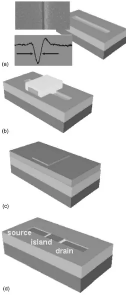
sim-plify the CMP process. The electron beam directly irradiates the SiO2layer, modifying its density8and, as a consequence, its etch rate in a dilute acid solution. The irradiated areas etch faster than the background, leading to trench formation. The trenches are not designed to reach the silicon substrate and the underlying oxide ensures electrical isolation from the substrate. When this isolation layer is reduced to a few tens of nanometers in thickness, it can also be used as a back-gate dielectric layer. The shape of the device after this step is a narrow trench in the oxide less than 15 nm wide by 25 nm deep, as shown in Fig.1共a兲. The depth of the trench is en-tirely controlled by the lithography exposure dose and can be precisely adjusted according to design needs.
Figure 1共b兲 shows how the SET island is created by patterning a Ti line perpendicular to the oxide trench. The line is oxidized in pure oxygen to grow 2 to 12 nm of TiOx
depending on oxidation time and temperature. This TiOxon
the Ti line sidewalls constitutes the tunnel junction dielectric layer. The width of the Ti line will determine the length of the SET island and contributes to its self-capacitance. This line can be patterned with reduced resolution requirements without compromising the total SET capacitance CT, which
must meet the subattofarad target required for wide range temperature operation. This relaxation of the resolution re-quirement is due to the fact that the tunnel junction capaci-tances of this process are extremely small as a result of the self-aligned fabrication technique. This represents a key ele-ment of this SET concept. In this work, EBL combined with a lift-off technique was used for patterning the Ti lines, with a resolution ranging from 50 to 75 nm.
In the last process step, a Ti layer called the blanket layer is deposited over the entire device area, as shown in Fig.
1共c兲. The substrate is fixed to a polishing jig and put face down on a turning polishing pad for chemical mechanical polishing. This planarization process will eliminate all mate-rial located above the surface of the thermally grown SiO2
a兲Electronic mail: [email protected]
APPLIED PHYSICS LETTERS 90, 113104共2007兲
layer. The top of the island is thus removed but its TiOx
sidewalls continue to isolate it from the rest of the thin line, which is now embedded in the SiO2. The end result is
pre-sented in Fig.1共d兲. The CMP process is stopped when test structures placed next to the SETs begin to disappear. This is because they intentionally received a lower exposure dose and are thus a few nanometers shallower that the SETs trench. We are investigating the use of stopping layers to improve the polishing accuracy, but with the current method, this optical end point strategy was quite easy to detect and control. The CMP process leads to the simultaneous forma-tion of the source, drain, and island of the SETs with a thick-ness of only 2 – 3 nm. Depending on the specific design of the devices, larger source and drain electrodes can then be deposited to facilitate the electrical characterization of the SETs.
The source-drain current IDSmeasured at room
tempera-ture is presented in Fig.2共a兲for two different back-gate bias values turning the device on and off. The inset of Fig.2共a兲
shows the SET characteristics under a wider VDSrange. The behavior of the IDS-VDScurves is strongly nonlinear for both
symmetrical and asymmetrical transistors with relatively high current drive in the nanoampere range. The asymmetri-cal case is a design with SET neighboring features that create localized uneven polishing, resulting in rounding of one of the junctions and thus in conductance differences. Other
IDS-VDS curves were obtained on a symmetrical layout and
one example is presented in Fig.2共b兲. We also scanned the back-gate bias and observed a transistor effect. The drain current is modulated by the back-gate voltage and showed regular oscillations, as presented in Fig.3. We have observed a back-gate leakage through the backside oxide on the samples with sub-100 nm thickness. The leakage is a back gate to source current of about 100 pA/ VGS and occurred after several temperature cycling tests. Metallic SETs are known to be surprisingly well described within a certain size range by a set of basic rules called the orthodox theory.9,10To model the devices at room temperature, we have used Monte Carlo simulations within this framework with capacitance
FIG. 1. Wide temperature SETs process overview.共a兲 View of the trench in the oxide layer and its top down SEM picture including the intensity profile showing where the linewidth is measured. Below the oxide layer is the silicon substrate used as a back gate.共b兲 The island formation. The open end drawing of the perpendicular Ti line shows the TiOxlayer grown on the
future island.共c兲 The titanium blanket layer is deposited. 共d兲 End result after CMP.
FIG. 2. Electrical characterization at room temperature.共a兲 Asymmetrical SET data with VGSat 0 V共䊐兲 and at 0.3 V 共䊊兲. The inset shows a wider
VDS range共䊐兲. The line represents the model calculations with CS= CD = 0.06 aF, RS= 1.7⫻107⍀, RD= 3.5⫻106⍀, and CGS= 0.23 aF.共b兲 Sym-metrical SET data with tunnel junction dielectric thickness of 12 nm for VGS at 0 V共䊐兲 and at 0.3 V 共䊊兲. The line represents the model calculation with CS= CD= 0.05 aF, RS= 6.3⫻108⍀, RD= 8.9⫻108⍀, and CGS= 0.3 aF.
FIG. 3. SET drain current behavior as a function of the back-gate bias at low drain voltage共25 mV兲. The line is the asymmetrical SET model and the squares共䊐兲 are the data. A dotted line is added as a guide to the eye. A gate to source leakage to of 100 pA/ VGSwas removed from the data to represent it on the same scale as the model.
and resistance values close to what is expected from the ge-ometry of the devices. The dimensions were extracted from measurements using a scanning electron microscope共SEM兲 and the oxide thickness was verified by ellipsometry. In the case of the asymmetrical transistor of Fig.2共a兲, the junction dimensions were 10 nm wide by 2 nm thick with an 8 nm layer of TiOxgrown at low temperature. The dielectric
con-stant of 3.5 of the titanium oxide was extracted from junction current curves as a function of electric field and temperature. This value is typical of an amorphous TiOx thin film.11,12
With a parallel plate model we evaluated the gate capaci-tance at 2.3⫻10−19F and the source and drain capacitances
at 7.7⫻10−20F. Considering the relative measurement error
of the SEM at this small size scale, these values are in good agreement with the model values which are 2.3⫻10−19F for
the gate capacitance and 6.0⫻10−20F for the source and
drain capacitances. These results confirmed that this self-aligned junction fabrication process is capable of subat-tofarad resolution. We have explored many scenarios and combinations of possible unexpected multiple junctions and conductance but none of them could explain our data other than Coulomb blockade arising from standard SET forma-tion. With this model, we have estimated our charging energy at 457 meV.
The IDS-VDS curve was then characterized as a function
of temperature and is presented in Fig.4. Measurements on the design with the highest charging energy were made up to the limit of the experimental setup at 433 K and the nonlin-earity attributed earlier to Coulomb blockade was still being observed. This is because the charging energy EC of
457 meV is still more than 12 times the value of thermal fluctuations at 433 K. Taking this same factor of 12 as a criterion for an initial approximation, one finds that even if
some fabrication steps deviate from nominal values and re-duce ECby 25% to 343 meV, Coulomb blockade could still
be observable up to around 330 K. This temperature reaches the upper specification limit of normal operation of many Si-FETs processes. It is then clear in this case that the SET operating temperature alone is not the limiting factor in hy-brid design fabrication. This conclusion is important for cir-cuit designers because it sets a value above room tempera-ture under which Coulomb blockade can be guaranteed.
The first three designs fabricated with this approach were all functional devices. A larger number of SETs based on this approach will need to be fabricated in order to evalu-ate the complete yield and repeatability of the process. Nev-ertheless, as an initial step, we have demonstrated the proof of concept of this method. Getting high temperature data gave us a valuable insight on how SETs evolve above room temperature and what kind of process tolerances will be re-quired to establish hybrid circuit fabrication. We also believe that this device platform might have some use to study and validate concepts of single charge tunneling theory at very high temperature.
The authors are grateful for grants from the Natural Sci-ences and Engineering Research Council of Canada. The au-thors also thank NanoQuébec and the Regroupement Québé-cois sur les Matériaux de Pointe for additional support for the nanofabrication infrastructure.
1K. Likharev, Proc. IEEE 87, 606共1999兲.
2Y. Takahashi, Y. Ono, A. Fujiwara, and H. Inokawa, J. Phys.: Condens. Matter 14, R995共2002兲.
3K. Miyaji, M. Saitoh, and T. Hiramoto, Appl. Phys. Lett. 88, 143505 共2006兲.
4Y. Ono, Y. Takahashi, K. Yamazaki, M. Nagase, H. Namatsu, K. Kurihara, and K. Murase, IEEE Trans. Electron Devices 47, 147共2000兲.
5A. Toriumi, K. Uchida, R. Ohba, and J. Koga, Physica B 272, 522共1999兲. 6K. S. Park, S.-J. Kim, I.-B. Baek, W.-H. Lee, J.-S. Kang, Y.-B. Jo, S. D. Lee, C.-K. Lee, J.-B. Choi, J.-H. Kim, K.-H. Park, W.-J. Cho, M.-G. Jang, and S.-J. Lee, IEEE Trans. Nanotechnol. 4, 242共2005兲.
7P. Xiaodan and A. Broers, J. Appl. Phys. 71, 6189共1992兲.
8J. R. Barnes, A. C. F. Hoole, M. P. Murrell, M. E. Welland, A. N. Broers, J. P. Bourgoin, H. Biebuyck, M. B. Johnson, and B. Michel, Appl. Phys. Lett. 67, 1538共1995兲.
9D. V. Averin and K. K. Likharev, in Mesoscopic Phenomena in Solids, edited by B. Altshuler, P. Lee, and R. Webb共Elsevier, Amsterdam, 1991兲, pp. 173–271.
10G. L. Ingold and Y. V. Nazarov, in Single Charge Tunneling, edited by H. Grabet and M. H. Devoret共Plenum, New York, 1992兲, pp. 21–108. 11K. Matsumoto, M. Ishii, J.-I. Shirakashi, K. Segawa, Y. Oka, B. J.
Varta-nian, and J. S. Harris, Tech. Dig. - Int. Electron Devices Meet. 1995, 363. 12F.-C. Chiu, S.-K. Fan, K.-C. Tai, J. Y. Lee, and Y.-C. Chou, Appl. Phys.
Lett. 87, 243506共2005兲. FIG. 4. SET curves as a function of temperature for the design with the
charging energy of 457 meV. Temperatures are 296 K共䊏兲, 316 K 共쎲兲, 336 K共䉱兲, 386 K 共䉲兲, and 433 K 共⽧兲. The back gate is grounded except for the open circles where VGSis 0.3 V at 433 K.