HAL Id: hal-01416945
https://hal.inria.fr/hal-01416945
Submitted on 15 Dec 2016
HAL is a multi-disciplinary open access
archive for the deposit and dissemination of
sci-entific research documents, whether they are
pub-lished or not. The documents may come from
teaching and research institutions in France or
abroad, or from public or private research centers.
L’archive ouverte pluridisciplinaire HAL, est
destinée au dépôt et à la diffusion de documents
scientifiques de niveau recherche, publiés ou non,
émanant des établissements d’enseignement et de
recherche français ou étrangers, des laboratoires
publics ou privés.
Adaptive Overclocking and Error Correction Based on
Dynamic Speculation Window
Rengarajan Ragavan, Cedric Killian, Olivier Sentieys
To cite this version:
Rengarajan Ragavan, Cedric Killian, Olivier Sentieys. Adaptive Overclocking and Error Correction
Based on Dynamic Speculation Window. ISVLSI, Jul 2016, Pittsburgh, United States. pp.325 - 330,
�10.1109/ISVLSI.2016.13�. �hal-01416945�
Adaptive Overclocking and Error Correction based
on Dynamic Speculation Window
Rengarajan Ragavan
University of Rennes 1, INRIA/IRISA Lannion, France
Cedric Killian
University of Rennes 1, INRIA/IRISA Lannion, France
Olivier Sentieys
INRIA/IRISA, University of Rennes 1 Lannion, France
Abstract—Error detection and correction based on double-sampling is used as common technique to handle timing errors while scaling Vdd for energy efficiency. An additional sampling
element is inserted in the critical paths of the design, to dou-ble sample the outputs of those logic paths at different time instances that may fail while scaling the supply voltage or the clock frequency of the design. However, overclocking, and error detection and correction capabilities of the double sampling methods are limited due to the fixed speculation window which lacks adaptability for tracking variations such as temperature. In this paper, we introduce a dynamic speculation window to be used in double sampling schemes for timing error detection and correction in pipelined logic paths. The proposed method employs online slack measurement and conventional shadow flipflop approach to adaptively overclock or underclock the design and also to detect and correct timing errors due to temperature and other variability effects. We demonstrate this method in the Xilinx Virtex VC707 FPGA for various benchmarks. We achieve a maximum of 71% overclocking with a limited area overhead of 1.9% LUTs and 1.7% flip-flops.
I. INTRODUCTION
Dynamic voltage and frequency scaling became the promi-nent way to reduce the energy consumption in digital systems by trading the performance of the system to an acceptable margin. Effect of scaling coupled with variability issues make highly pipelined systems more vulnerable to timing errors [1]. Such errors have to be corrected at the cost of additional hard-ware for proper functioning [2]. The Razor method proposed in [3] is a very popular error detection and correction architecture for timing errors in digital systems, inspired from the more general double-sampling technique [2]. In the double-sampling architecture, an additional sampling element, known as shadow register, is used along with the main output register to sample the output at different timing instances. The shadow registers are clocked by a delayed version of the main clock known as the shadow clock. The timing interval between the rising edges of the main clock and the shadow clock is termed as the speculation window (φ).
There is a trade-off between width of the speculation window and fault coverage. For a wider speculation window, more errors could be detected and corrected, but this requires more buffer insertion for logic paths that are shorter than the speculation window. And vice-versa for a narrower speculation windows. Designs with fixed speculation window optimized for certain operating condition might suffer from an increased error rate under variability issues such as thermal effects. In order to tackle these limitations, double-sampling technique
with dynamic speculation window is required to adpatively vary the speculation window with respect to the variability effects. Razor-like fault detection and correction techniques are used in reconfigurable architectures like FPGAs (Field-Programmable Gate Arrays) and CGRAs (Coarse-Grain Re-configurable Arrays) due to moderate clock frequencies and function-specific pipelines [4], [5]. All these existing methods use a fixed speculation window for the double sampling and overclocking of the system without any adaptive feedback to tackle the variability effects.
In this paper, we propose to use a dynamic speculation window in double-sampling schemes for error detection and correction in pipelined logic paths. An FPGA prototype is used as proof of concept, though the idea can be extended to any type of datapaths. The proposed method is based on double-sampling and online slack measurement [6] to overclock and underclock the design adaptively according to temperature and other variability effects, and therefore to detect and correct tim-ing errors. Addition of buffers for shorter path is not required, since the speculation window is dynamically changed. Results show that a maximum of 71% overclocking is achieved with a limited area overhead of 1.9% LUTs and 1.7% flip-flops.
The paper is organized as follows. Section II presents overclocking and timing error detection in FPGA and the pro-posed dynamic speculation window architecture is described in Section III. Experimental results are given in Section IV, related works are discussed in Section V and finally Section VI gives some conclusions and perspectives.
II. OVERCLOCKING ANDERRORDETECTION INFPGAS
A. Impact of Overclocking in FPGAs
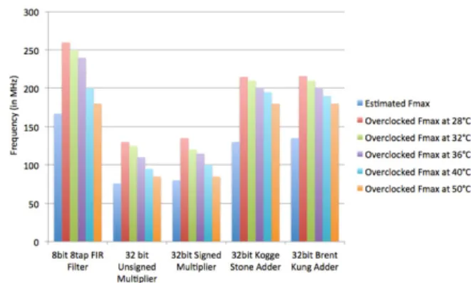
In general, FPGA designs can be safely overclocked by a significant ratio with respect to the maximum operating fre-quency estimated by the FPGA’s synthesis and place-and-route tool flow. This gives the advantage of increasing the imple-mentation throughput without any design-level modifications. As a motivating example, an 8-bit 8-tap FIR (Finite Impulse Response) digital filter was synthesized and implemented in the Xilinx Virtex VC707 evaluation board. The maximum operating clock frequency estimated by Vivado 2014.4 tool flow, with performance optimized synthesis, is 167 MHz. A test bench is created with a 80-bit LFSR, feeding random input patterns to the design, and the output of the design is monitored using Vivado’s Integrated Logic Analyzer (ILA). A functional simulation output obtained from RTL simulation is used to
Fig. 1. Timing errors (percentage of failing critical paths and output bit error rate) vs. Overclocking in FPGA configured with an 8-bit 8-tap FIR filter
compare the output of the ILA. Onboard IIC programmable LVDS (Low-Voltage Differential Signaling) oscillator is used to provide clock frequency for the pattern generator and the design under test. At the ambient temperature, the clock frequency is increased from 160 MHz to 380 MHz and the output data is recorded for all the frequency steps.
Fig. 1 shows the evolution of bit error rate at the output of the design with respect to overclocking. In Fig. 1, the first plot (orange squares) represents the percentage of critical paths that fail when the FPGA is overclocked. Similarly, the second curve (blue diamonds) represents the output Bit Error Rate (BER), defined as the percentage of false output bits. As shown in Fig. 1, there are no errors recorded until 260MHz, which gives the safe overclocking margin of 55% with respect to the maximum operating frequency estimated by Vivado, and therefore a performance gain of 1.55×. Beyond this safe overclocking margin, some critical paths in the design starts to fail and the output error rate increases exponentially with respect to the increase in the clock frequency. Overclocking up to 300 Mhz (×1.8 the operating frequency) leads to BER of 10%, which would be still acceptable for applications that tolerate approximate computations [7]. Around 350 MHz, all critical paths fail and the bit error rate converges to 40%. By employing error detection and correction mechanisms, such as double-sampling methods, FPGA designs can therefore be adaptively overclocked to improve performance at run time, according to varying operating conditions (e.g., temperature). B. Double Sampling
Error detection based on the double-sampling scheme requires less area and power overhead than traditional con-current detection methods such as Double Modular Redun-dancy (DMR) [2]. In the double-sampling method, instead of replicating the entire pipeline, an additional sampling element (latch or flip-flop) is added at the output of the pipeline to sample the output data at two different time instances using the main clock (Mclk) and a shadow clock (Sclk). In
Fig. 2, a logic path P ath1 is constrained between the input
register R1 and the output register Q1. An additional shadow
register S1 also samples the output data at different timing
instance. An XOR gate is used to compare the data from the registers Q1 and S1. An error register E1 is used to record
any discrepancies between output data from Q1 and S1. The
multiplexer M1 is used to select the valid output for error
correction based on error signal from the register E1. Different
versions of double-sampling methods, such as [8], Razor [3],
Fig. 2. Principle of the double-sampling method to tackle timing errors
Fig. 3. Principle of online slack measurement for overclocking
RazorII [9], Bubble Razor [10], GRAAL [11] have emerged and are commonly used in digital designs for detecting timing errors and counteracting the effect of dynamic voltage and frequency scaling (DVFS).
All the doubling sampling techniques use a fixed spec-ulation window and the detected errors are corrected either by copying the valid output from the shadow register or architecture replay technique is used. Due to the fixed specu-lation window, there is no dynamicity in these methods, which cannot adaptively change the frequency of the design in both directions (overclocking and underclocking) at run time. Since the shadow clock always lags behind the main clock, when the critical paths in the design fails to meet the timing constraints due to the temperature or other variability effects, the shadow register can detect and correct the errors. However, the fixed speculation window does not give the adaptability to measure the slack and to overclock the design. Also, in methods like Razor [3], additional buffers are needed for logic paths that are shorter than the speculation window, which results in increased area overhead.
C. Slack Measurement
In [6], [12], and [13], online slack measurement techniques are proposed to determine the delay of the combinational components in the pipeline at run time. An additional sampling register is added to the output of the pipeline, which samples the data before the main output register of the pipeline. As shown in Fig. 3, the output of the pipeline P ath1is sampled by
both main register Q1 and shadow register T1 using the main
clock Mclkand the shadow clock Sclkrespectively. Both Mclk
and Sclkare of same clock frequency but with different phases.
This method is very similar to the double sampling technique discussed in the previous subsection. The only difference is that the shadow clock Sclk always leads the main clock Mclk
by a phase difference φ. An XOR gate is used to compare the outputs from both main register Q1 and shadow register T1.
Output of the XOR gate is sampled by error register e1. To
determine the available positive slack of the pipeline P ath1,
the phase difference φ is increased until the error register e1
records an error. Due to the leading shadow clock, this method is not capable of detecting timing errors in the critical paths that violate timing constraints due to temperature or other variability effects.
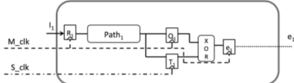
Fig. 4. Principle of the dynamic speculation window based double-sampling method. Solid lines represent data and control between modules, dashed lines represent main clock, dash-dot-dash lines represent shadow clock, and dotted lines represent feedback control
III. PROPOSEDMETHOD FORADAPTIVEOVERCLOCKING
In this work, we propose to use a dynamic speculation window combined with the double-sampling method for error detection and correction and accordingly to adaptively over-clock and underover-clock the design based on variability effects. The following sections present the proposed architecture of a dynamic speculation window and then our adaptive feedback loop for over-/under-clocking the design.
A. Dynamic Speculation Window Architecture
Fig. 4, shows the schematic of the proposed dynamic speculation window architecture. A design composed of n logic paths is annexed with two shadow registers. The number of logic paths n is pre-determined as the percentage of the critical delay margin. In the rest of this section, we consider one path P ath1out of n paths. As shown in Fig. 4, logic path
P ath1 is constrained between input register R1 and output
register Q1. Two shadow registers S1 and T1 are added to
sample the output of the P ath1, in contrast to the one shadow
register approach in [4], [5], and [14]. T1 is used to measure
the available slack in the path which is used to overclock the design, while S1 is used to sample the valid data, when the
delay of the P ath1 is not meeting the timing constraints of
the main clock M clk due to the variability effects. As like double-sampling architectures, it is assumed that the shadow register S1 always samples the valid data. In this setup, all
three registers S1, Q1 and T1 use the same clock frequency
but different phases to sample the output. The main output register Q1 samples the output at the rising edge of M clk,
while shadow register S1 samples the output at the falling
edge of M clk. Shadow register T1 samples the output in
the rising edge of the shadow clock S clk generated by the phase generator. Two XOR gates compare the data in main and shadow registers S1and T1, the corresponding error values are
registered in E1 and e1. The registers E1 and e1 are clocked
by falling and rising edge of the M clk respectively.
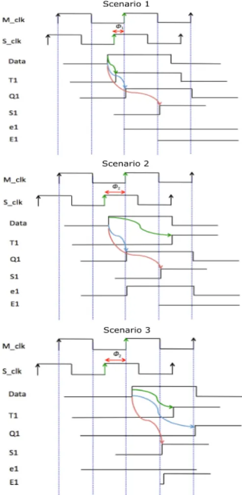
Fig. 5 shows the timing diagram of the proposed method. In Scenario 1, the shadow clock (S clk) leads the main clock (M clk) by phase φ1. Since the Data (output of P ath1) is
available before the rising of the shadow clock, the valid data is
sampled by T1. Registers Q1and S1also sample the valid data
in the rising and falling edges of the main clock respectively. Since the main and shadow registers sampled the same data, e1
and E1 are held at logic zero representing no timing error. In
Scenario 2 shown in Fig. 5, the shadow clock leads the main clock by a wider phase φ2, which results in invalid data being
sampled by T1, while Q1and S1sample the valid data. In this
case, the error signal e1 is asserted at the rising edge of the
main clock, while E1is still at logic zero, which indicates the
overclocking using speculation window greater than or equal to φ2 will result in errors. In Scenario 3 shown in Fig. 5, due
to temperature or other variability effects, the logic delay of the P ath1 violates the timing constraints of both the shadow
and main clocks. This results in wrong data getting sampled by the shadow register T1 and main register Q1. The shadow
register S1 samples the valid data since Data is valid before
the falling edge of the main clock. Since both T1 and Q1
sample wrong data, e1is not asserted, while E1is asserted due
to the difference between Q1 and S1 registers. Fig. 4 shows
the schematic of error correcting mechanism in the proposed method. Here the outputs of the main register Q1 and the
shadow register S1are connected to the multiplexer M1. When
the error signal E1 is equal to zero, multiplexer output M1
passes output of Q1. When E1 is held high, the output of S1
is passed to the next stage of the pipeline.
Scenario 1
Scenario 2
Scenario 3
Fig. 5. Timing diagram of proposed method. Scenario 1: Slack measurement phase. Scenario 2: Maximum overclocking margin. Scenario 3: Impact of temperature at maximum overclocking frequency
B. Adaptive Over-/Under-clocking Feedback Loop
Fig. 4 shows the feedback loop of the proposed method. The error signals Ei and ei from all the monitored paths are
connected to Error Counter and Slack Counter respec-tively. For different speculation windows φi, Error Counter
and Slack Counter count the discrepancies in the paths being monitored. The Slack Counter margin defines the amount of errors that can be tolerated while overclocking the design and the Error Counter margin defines the amount of error that can be tolerated due to variability effects. Tolerable error mar-gin of Error Counter and Slack Counter are determined from the timing reports after synthesis and placement of the design. After, the synthesized bitstream is programmed into the FPGA and the design is intially clocked at the maximum frequency (Fmax) estimated by Vivado.
In this paper, we have implemented error-free overclocking, therefore Slack Counter margin is set to zero. At the ambient core temperature of around 28◦C, when Error Counter and Slack Counter are equal to zero, the speculation window φ is increased for every clock cycle from 0◦ to 180◦ at discrete intervals of 25◦ until the Slack Counter records an error. Beyond 180◦up to 360◦, the speculation window width repeats due to periodic nature of the clock. Once the slack counter records an error, the system is put on halt and safely over-clocked by trading the available slack. While the speculation window φ is swept, the pipeline functions normally since the output register Qiand the shadow register Si sample the same
valid data. Regarding error correction due to variability effects, if Error Counter records more than 2% of the monitored paths not meeting the timing constraints, the system is put on halt and the operating frequency of the system is decreased in multiples of a clock frequency step δ to reduce the errors (in our test platform the frequency step is δ = 5M Hz). Since correcting more errors will reduce the throughput of the design, decreasing the operating frequency is a necessary measure. Multiplexer Mi, as shown in Fig. 4, corrects the error by
connecting the output of the shadow register Si to the next
stage of the pipeline. Once the temperature falls back, the operating frequency of the design is again increased based on the slack measurement as described earlier.
IV. EXPERIMENTS AND RESULTS
The proposed Dynamic Speculation Window in the double-sampling method is implemented in a Xilinx Virtex VC707 evaluation board. Vivado tool flow is used to synthesize and implement the RTL benchmarks into the FPGA. A testbench is created for all the benchmark designs with an 80-bit LFSR pattern generator for random inputs to the design under test. Onboard IIC programmable LVDS oscillator is used to provide clock frequency for the pattern generator and the design under test. As shown in Fig. 4, control signals from the Error Counter and the Slack Counter determine the output frequency of the LVDS oscillator. Different phases of the gen-erated clock frequency are obtained from the inbuilt MMCM (Mixed-Mode Clock Manager) module in the FPGA [15]. The core temperature is monitored through XADC system monitor, and the temperature is varied by changing the cooling fan speed.
To highlight the adaptive overclocking and timing error detection and correction capability of the proposed method,
Fig. 6. Overclocking versus temperature for different benchmarks
we have implemented a set of benchmark designs in both Razor-based method and the proposed dynamic speculation window based method. Benchmarks used in this experiments are common datapath elements like FIR filter (8 taps, 8 bits), and various versions of 32-bit adder and 32-bit multiplier ar-chitectures. After implementation, timing reports are generated to spot the critical paths in the design. Table I shows the area footprint and the maximum operating frequency determined by the Vivado tool flow. Timing and location constraints are used to place the shadow registers Siand Ti close to the main
output register Qi for all the output bits of the design. For the
Razor-based method, all the monitored paths are annexed with one shadow register Siin contrast to the proposed method with
two shadow registers, and the logic paths that are shorter than speculation window are automatically annexed with buffers by the synthesis tool. For comparison purpose, both the Razor-based method and the proposed method are subjected to identical test setup. In the Razor-based method, the design is overclocked beyond the maximum frequency estimated by Vivado and the FPGA’s core temperature is varied to introduce variability effects in the design. Online slack measurement is not used in the Razor-based method to show how the proposed method with slack measurement can adaptively overclock as well as underclock under identical test setup.
In the proposed method, after the synthesized bitstream is programmed into the FPGA, the design is clocked at Fmax
estimated by Vivado. At the ambient core temperature of around 28◦C, the speculation window φ is increased for every clock cycle and if the Slack Counter is zero at the widest speculation window, then the clock frequency can be increased up to 40%, because at 180◦, φ corresponds to half of the clock period. That implies all the critical paths in the design have positive slack equals to half of the clock period. Overclock-ing is done by haltOverclock-ing the design and increasOverclock-ing the clock frequency from the LVDS oscillator. The LVDS oscillator is programmed through the IIC bus with the pre-loaded command word for the required frequency. After changing the frequency, again the phase sweep starts from 0◦until the Slack Counter records an error. This way, the error-free overclocking margin of each design is determined with respect to the maximum operating frequency estimated by Vivado.
While operating at the safe overclocking Fmaxat 28◦C, the
core temperature of the FPGA is varied by changing the speed of the cooling fan. Due to the increase in temperature, the criti-cal paths of the design starts to fail. When the Error Counter records error in more than 2% of the monitored paths, the
TABLE I. SYNTHESIS RESULTS OF DIFFERENT BENCHMARK DESIGNS
Benchmarks Area without error detectionLUTs Flip-Flops (FFs) Area overhead for proposed methodLUTs Flip-Flops Area overhead for RazorLUTs Flip-Flops Estimated Fmax(MHz)
8-tap 8-bit FIR Filter 1279 1547 2.5% 2% 2% 1% 167
Unsigned 32-bit Multiplier 7270 4511 1.9% 1.7% 2.3% 0.9% 76
Signed 32-bit Wallace Tree Multiplier 5997 4458 2.8% 1.8% 3.2% 1% 80
2-bit Kogge-Stone Adder 3944 4117 3.7% 1.7% 4% 1.2% 130
32-bit Brent-Kung Adder 3753 4053 3.3% 1.9% 3.8% 1% 135
TABLE II. IMPACT OF TEMPERATURE WHILE OVERCLOCKING IN BENCHMARK DESIGNS
Benchmarks
Safe overclocking Safe overclocking % of monitored paths Safe overclocking Safe overclocking Fmaxat 28◦C margin fails at 50◦C Fmaxat 50◦C margin
(in MHz) at 28◦C for Fmaxat 28◦C (in MHz) at 50◦C
8-tap 8-bit FIR Filter 260 55% 12 180 8%
Unsigned 32-bit Multiplier 130 71% 22 85 12%
Signed 32-bit Wallace Tree Multiplier 135 69% 26 85 7%
32-bit Kogge-Stone Adder 215 64% 13 180 38%
32-bit Brent-Kung Adder 216 60% 21 180 33%
design is put on halt and the frequency is reduced in multiples of 5MHz until the Error Counter margin is below 2%. Since the shadow register Si latches the correct output, errors are
corrected without re-executing for that particular input pattern. The tolerance margin is used to reduce the overhead in error correction mechanism which can affect the throughput of the design.
Table I provides synthesis results on the benchmarks with-out any error detection technique, with razor flip-flops [4], and with proposed error detection and correction technique. The area overhead of the proposed method compared to the original design is kept between 3.6% to 5.4%, which demonstrates the applicability of the technique in real designs. Table I also provides the maximal frequency Fmax estimated by Vivado.
The Look-Up Table (LUT) overhead of the proposed method is on average 0.4% less compared to the Razor implementation, since no buffers are needed for the shorter paths. However, Flip-Flop (FF) overhead of the proposed method is 0.8% more compared to the Razor method due to the two shadow flip-flops used for slack measurement and error correction.
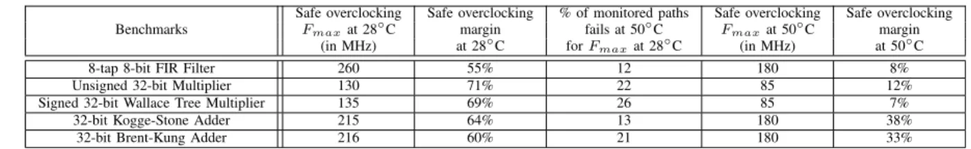
Fig. 6, shows the plot of safe overclocking frequency of all the benchmark designs that can be reached by the proposed error detection method for different FPGA’s core temperature. As an example, for the FIR filter design, Vivado estimated Fmax is 167MHz. However this design can then
be overclocked at the ambient temperature of 28◦C by more than 55% up to 260MHz, without any error, and up to 71% for the other benchmarks. At the safe overclocking frequency, the temperature is increased from 28◦C to 50◦C at which Error Counter records 12% of the paths failed. Since the percentage of failing paths is more than the determined margin of 2%, the clock frequency of the LVDS oscillator is brought down to 180MHz, as shown in Table II, which results in a percentage of failing paths below 2%. Once the temperature falls back to 28◦C, the available slack is measured and the clock frequency is increased again to 260MHz.
Table II lists the impact of temperature and the safe over-clocking margin at the ambient temperature of 28◦C and high temperature of 50◦C for all the benchmarks. The percentage of monitored paths that fails at 50◦C shows the impact of the temperature while overclocking the design. The operating frequency has to be scaled down to limit these errors which
can be eventually corrected by the error correction technique in the proposed method. Even at the higher temperature of 50◦C, the FIR filter is safely overclocked up to 8% compared to the maximum frequency estimated by Vivado. Similarly, at 50◦C, both unsigned and signed multiplier architectures can be safely overclocked up to 12% and 7% respectively. A maximum safe overclocking margin of 38% is achieved for the Kogge-Stone adder and 33% by the Brent-Kung adder while operating at 50◦C. These results demonstrate the overclocking and error detection / correction capability of the proposed method with a limited area overhead in the FPGA resources.
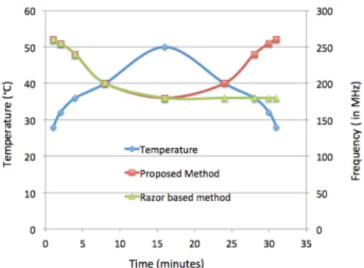
Fig. 7, shows the comparison of the proposed dynamic speculation window and the Razor-based overclocking for the 8-bit 8-tap FIR filter design in Virtex 7 FPGA. As shown in Fig. 7, the core temperature of the FPGA is varied by controlling the cooling fan of the FPGA. The FPGA’s core temperature is increased from the ambient room temperature of 28◦C to 50◦C and then decreased again back to the room temperature. When the temperature increases, critical paths in the design starts to fail, which makes the proposed method and the Razor-based method to scale down the frequency to limit the error below 2% of monitored paths. Initially, at the room temperature, the design is running at 260 MHz. At the tem-perature of 50◦C, the frequency is scaled down to 180 MHz. When the temperature falls back to the room temperature, the proposed method is able to measure the available slack in the pipeline and to increase the frequency to overclock the design and therefore to increse performance. Under similar test setup, the Razor-based feedback loop scales down the frequency as the temperature increases. However, when the temperature falls back, there is no change in the frequency. This is because the Razor implementation does not have the slack measurement in place to adaptively change the frequency when the temperature is reducing. Due to the additional shadow register placed in the proposed method, the system is able to measure the slack available in the pipeline which is traded to overclock the design according to temperature fluctuations. From Table 6, we can observe a 0.78% difference in terms of area overhead between the proposed method and the Razor implementation, on average. This gives more upper hand for the proposed dynamic speculation window based error detection method over the classical Razor-based timing error detection.
Fig. 7. Comparison of Razor-based feedback look and the proposed dynamic speculation window. Curve in blue diamond represents the FPGA’s core temperature. Curve in red square represents the frequency scaling by the proposed method. Green triangle curve represents the frequency scaling by the Razor-based method
V. RELATEDWORK
A. DVFS with slack measurement
In [14], an online slack measurement technique based on [6], [12], and [13] is used to scale the supply voltage or frequency to increase the energy savings. The output of the path under monitoring (PUM) is sampled by both main register and shadow register using same clock frequency but different phases as shown in Fig. 3. The measured slack is compared with the pre-determined guardband to increase the energy savings by scaling the voltage or frequency. This method is providing energy saving without any scope for error detection or correction. Since the shadow clock is leading the main clock, it cannot detect the error when the critical path violates the main clock timing constraints due to temperature and other variability effects.
B. Timing error handling in FPGA and CGRA
In [4], the advantages of using Razor-based error detection and correction in FPGA implementations to increase energy efficiency are discussed. In this method, a timing fault detector (TFD) is added to the pre-determined number of logic paths in the FPGA implementation. After placing the TFDs, the FPGA is overclocked beyond the maximum frequency estimate given by the FPGA timing tool under fixed temperature and supply voltage. Scope of this method is only detecting the fault rate for different frequencies beyond the maximum frequency. No error correction technique is proposed nor the variability issues are discussed.
In [5], overclocking CGRAs using Razor is presented. This method focuses on implementing Razor in 2D arrays and propagating stall signals to correct the errors due to overclocking. However, this method is also not discussing about adaptively changing the frequency based on temperature and variability effects. Similarly, [16] presents timing error handling in CGRAs using triple modular redundancy (TMR). Hardware redundancy methods consume more power and area compared to time redundancy methods.
VI. CONCLUSION
In this paper, we have proposed to use a dynamic specula-tion window in double-sampling for error detecspecula-tion and correc-tion, and implemented this method in an FPGA prototype. The
proposed design uses double-sampling and slack measurement to adaptively overclock the design. The maximum of 71% safe overclocking margin at ambient temperature has been achieved at the cost of shadow registers, XOR gates, and counters, which results in a maximum area overhead of 1.9% LUTs and 1.7% FFs over the original design, as shown in Table I. Instead of merely overclocking the design this method detects timing errors and corrects it in real time. This method can be easily expanded to other form of datapaths and also reconfigurable architecture like CGRAs.
REFERENCES
[1] E. Stott, Z. Guan, J. M. Levine, J. S. Wong, and P. Y. Cheung, “Variation and reliability in FPGAs,” IEEE Design & Test, vol. 30, no. 6, pp. 50– 59, 2013.
[2] M. Nicolaidis, “Double-sampling design paradigma compendium of architectures,” IEEE Trans. on Device and Materials Reliability, vol. 15, no. 1, pp. 10–23, 2015.
[3] D. Ernst, S. Das, S. Lee, D. Blaauw, T. Austin, T. Mudge, N. S. Kim, and K. Flautner, “Razor: circuit-level correction of timing errors for low-power operation,” IEEE Micro, vol. 24, no. 6, pp. 10–20, 2004. [4] E. Stott, J. M. Levine, P. Y. Cheung, and N. Kapre, “Timing fault
detection in FPGA-based circuits,” in Proc. IEEE Int. Symp. on Field-Programmable Custom Computing Machines (FCCM), 2014, pp. 96–99. [5] A. Brant, A. Abdelhadi, D. H. Sim, S. L. Tang, M. X. Yue, and G. G. Lemieux, “Safe overclocking of tightly coupled CGRAs and processor arrays using razor,” in Proc. IEEE Int. Symp. on Field-Programmable Custom Computing Machines (FCCM), 2013, pp. 37–44.
[6] J. M. Levine, E. Stott, G. Constantinides, P. Y. Cheung et al., “SMI: Slack measurement insertion for online timing monitoring in FPGAs,” in Proc. Int. Conf. on Field Programmable Logic and Applications (FPL), 2013, pp. 1–4.
[7] A. Yazdanbakhsh, D. Mahajan, B. Thwaites et al., “Axilog: Language support for approximate hardware design,” in Proc. of the Design Automation & Test in Europe Conf. (DATE), 2015, pp. 812–817. [8] M. Nicolaidis, “Time redundancy based soft-error tolerance to rescue
nanometer technologies,” in Proc. 17th IEEE VLSI Test Symp., 1999, pp. 86–94.
[9] S. Das, C. Tokunaga, S. Pant, W.-H. Ma, S. Kalaiselvan, K. Lai, D. M. Bull, and D. T. Blaauw, “RazorII: In situ error detection and correction for pvt and ser tolerance,” IEEE Journal of Solid-State Circuits, vol. 44, no. 1, pp. 32–48, 2009.
[10] M. Fojtik, D. Fick, Y. Kim, N. Pinckney, D. M. Harris, D. Blaauw, and D. Sylvester, “Bubble razor: Eliminating timing margins in an arm cortex-m3 processor in 45 nm cmos using architecturally independent error detection and correction,” IEEE Journal of Solid-State Circuits, vol. 48, no. 1, pp. 66–81, 2013.
[11] M. Nicolaidis, “Graal: a new fault tolerant design paradigm for mit-igating the flaws of deep nanometric technologies,” in IEEE Int. Test Conference (ITC), 2007, pp. 1–10.
[12] J. S. Wong, P. Sedcole, and P. Y. Cheung, “Self-measurement of combinatorial circuit delays in FPGAs,” ACM Trans. on Reconfigurable Technology and Systems (TRETS), vol. 2, no. 2, p. 10, 2009. [13] P. Sedcole, J. S. Wong, and P. Y. Cheung, “Characterisation of FPGA
clock variability,” in IEEE Computer Society Annual Symp. on VLSI (ISVLSI), 2008, pp. 322–328.
[14] J. M. Levine, E. Stott et al., “Online measurement of timing in circuits: For health monitoring and dynamic voltage & frequency scaling,” in Proc. IEEE Int. Symp. on Field-Programmable Custom Computing Machines (FCCM), 2012, pp. 109–116.
[15] Xilinx, VC707 Evaluation Board for the Virtex-7 FPGA User Guide, v1.6 ed., April 2015.
[16] T. Schweizer, W. Rosenstiel, L. Vaz Ferreira, and M. Ritt, “Timing error handling on CGRAs,” in Proc. Int. Conf. on Reconfigurable Computing and FPGAs (ReConFig), 2013, pp. 1–6.