HAL Id: tel-01433533
https://pastel.archives-ouvertes.fr/tel-01433533
Submitted on 12 Jan 2017HAL is a multi-disciplinary open access
archive for the deposit and dissemination of sci-entific research documents, whether they are pub-lished or not. The documents may come from teaching and research institutions in France or abroad, or from public or private research centers.
L’archive ouverte pluridisciplinaire HAL, est destinée au dépôt et à la diffusion de documents scientifiques de niveau recherche, publiés ou non, émanant des établissements d’enseignement et de recherche français ou étrangers, des laboratoires publics ou privés.
structures et dispositifs III-N
Marco Piccardo
To cite this version:
Marco Piccardo. Spectroscopie des processus photoélectriques dans les structures et dispositifs III-N. Autre [cond-mat.other]. Université Paris Saclay (COmUE), 2016. Français. �NNT : 2016SACLX056�. �tel-01433533�
NNT : 2016SACLX056
T
HESE DE DOCTORAT
DE
L’U
NIVERSITE
P
ARIS
-S
ACLAY
PREPAREE A
L
’E
COLE
P
OLYTECHNIQUE
ECOLE DOCTORALE N° 573
Interfaces : approches interdisciplinaires/fondements, applications et innovations
Spécialité de doctorat : Physique
Par
M. Marco Piccardo
Spectroscopy of photoelectric processes in III-N structures and devices
Thèse présentée et soutenue à Palaiseau, le 23 septembre 2016 :
Composition du Jury :
M. Jean-Michel GERARD, Professeur CEA-INAC Président
M. Jean-Yves DUBOZ, Directeur de Recherche CNRS-CRHEA Rapporteur M. Nicolas GRANDJEAN, Professeur EPFL (Suisse) Rapporteur M. Luca PERFETTI, Professeur Ecole Polytechnique-LSI Examinateur M. Jacques PERETTI, Directeur de Recherche Ecole Polytechnique-PMC Directeur de thèse M. Lucio MARTINELLI, Ingénieur de Recherche Ecole Polytechnique-PMC Co-directeur de thèse M. Claude WEISBUCH, Professeur Ecole Polytechnique/UCSB Co-directeur de thèse M. James S. SPECK, Professeur UCSB (Etats Unis) Invité
To my father,
For daydreaming, from time to time, about me
“The end of one journey is simply the start of another. […] You have to start the journey anew. Always.”
A
CKNOWLEDGEMENTS
First of all I would like to thank my advisors: Prof. Claude Weisbuch, Dr. Jacques Peretti and Dr. Lucio Martinelli.
Claude is the dream of any ambitious young scholar. He is a coach, a wide-ranging master. I would like to call him my Socrates: he bombarded me with questions – good questions – during my PhD, and in this way he helped me shaping my scientific thinking. Sometimes, even if he is not around me, I can hear him in my mind asking me questions. He has not only accompanied me in this journey through science but he has also always been ready to help me in my personal life, as a friend.
Jacques gave me a large freedom to work in research. And freedom has an immeasurable value in science. When he intervened, he helped me adding profound value at the same time to my work and myself. To my work, thanks to his expertise and his perceptive vision of physics, and to myself, enhancing my career path and shaping my future.
Lucio, as everybody knows at the PMC laboratory, is magical. He is everywhere! Whenever I needed him, he appeared. And whatever the problem was, he helped me solving it. I have never seen him without a smile. He has also been a fundamental moral support for the success of my PhD.
During these years I have collaborated and discussed with several researchers at the PMC laboratory. I would like to thank in particular the following ones. Prof. Marcel Filoche, who supervised all the work in my thesis related to the localization landscape theory of disorder in semiconductors. As a theoretician, he has been an important reference for me during these years and with him I have enjoyed blackboards nicely filled with equations. I would also like to thank Dr. Fouad Maroun and Dr. Yves Lassailly, who never hesitated to give me some of their time, for discussing and working together to some experiment: Fouad, in the atomic-force microscopy measurements, and Yves, in the scanning tunneling microscopy measurements.
At the PMC laboratory I have experienced a wonderful atmosphere, thanks to all the people who animate this laboratory: the researchers, PhD students, post-docs and interns,
friends in the coffee room of the laboratory. Thanks in particular to all the students for their solidarity and optimism, and for all the good time spent together, skiing, running, playing poker, and so on.
During these years, I have spent seven months of research welcomed in the laboratories of Prof. James Speck and Prof. Shuji Nakamura at the University of California, Santa Barbara. I would like to thank in particular Jim for having transmitted me a sense of competition and excitement that is in resonance with my feelings in research. We had a wonderful discussion a couple of years ago in a restaurant about life and research that I will never forget. Thanks also to all the graduate students who provided me with the primary source for experiments, i.e. samples, in particular: Justin Iveland, Nathan Young, Leah Kuritzy, Daniel Myers, Abdullah Alhassan and Burhan Saifaddin.
The simulation studies presented in this thesis related to the localization landscape theory of disorder in semiconductors were carried out in strict collaboration with the group of Prof. Yuh-Renn Wu at the National Taiwan University. I would like to thank Yuh-Renn and his team, in particular Dr. Chi-Kang Li, for the frequent and fruitful discussions we had and for their kind availability at any moment.
I would also like to thank Dr. Luca Perfetti, who warmly welcomed me in his laboratory at the synchrotron Soleil and who allowed me to carry out experiments autonomously on his “Ferrary” of ultra-high vacuum, a great angle-resolved photoemission spectroscopy setup.
Finally let me get to the loved ones. Thanks to all my longtime friends with whom, despite the long distance, I still share glories and despairs.
It is not sufficient to thank my family. In Japan they say that, since our birth we have a debt with our family, due to its love and sacrifices, which we will never be able to pay back. Thanks to my mother, my father and my sister for having given me wings to fly. And to conclude, my love, because “Omnia vincit amor”. Thanks to my girlfriend, who simply completes me and allows me to be a three-dimensional man. Obrigado.
A
BSTRACT
itride light-emitting diodes (LEDs) have triggered a real revolution in lighting. Rapid technological progress has led to very high efficiencies with recent records exceeding 300 lm/W in the case of white LEDs. But in spite of these exceptional performances, recognized by the Nobel Prize in Physics in 2014, the intrinsic properties of nitride alloys and the physics of these devices are still not well understood. Carrier dynamics and nonlinear phenomena play a fundamental role on LED performance under high injected current, but electrical measurements can hardly give access to transport processes occurring over a range of energy states larger than kBT without resorting to models and simulations. Besides, there is growing evidence that alloy disorder plays a major role in the electrical and optical properties of nitride materials. However, modelling the disorder-induced localization effects is a practically unrealizable task in the framework of nowadays existing methods and, in fact, device design tools accounting for these effects still lack. In the course of my thesis work, novel experimental and theoretical approaches to tackle the study of the microscopic mechanisms governing the electronic properties of nitride semiconductors have been developed.
The emission of electrons from nitride compounds and devices activated to negative electron affinity was studied under optical excitation and under electrical injection of carriers. This approach gives access to the whole conduction band by low energy electron spectroscopy techniques, thereby allowing selective identification of processes involved in the excitation and transport of electrons. Near band gap photoemission spectroscopy was performed to study the conduction band structure of GaN. These measurements provided, in particular, the first direct determination of the energy position of the side valleys of the band conduction. During this study, "anomalous" photoemission processes were also evidenced. In addition, electron emission from LED under electrical injection of carriers was studied. The origin of the various structures observed in the electroemission spectra is discussed and, in particular, the contribution of anomalous photoemission processes is evaluated.
A recent theory of localization in disordered systems is applied to nitride materials and optoelectronic devices. This method allows for the first time the determination of the localization landscape induced by alloy disorder without solving the Schrödinger equation associated with the disordered system, which leads to a strong reduction of the computation time. The modelling is developed to completely describe a device in operating condition. Experimentally, the problem of disorder-induced localization is approached by photocurrent spectroscopy measurements in LEDs and solar cells whose active regions contain InGaN quantum wells. A clear signature of alloy disorder is observed in the form of an exponential absorption tail (Urbach tail) for below-gap excitation. This allows defining a characteristic energy of the disorder which is found to be in excellent agreement with the predictions given by the novel localization theory. The application of this theory to the modelling of full 3D LED structures with compositional fluctuations allows computing self-consistently device characteristics including quantum effects.
R
ESUME DE THESE
es diodes électroluminescentes en nitrures (LED) ont déclenché une véritable révolution dans l'éclairage. Les progrès technologiques rapides ont conduit à des rendements très élevés, avec des records récents dépassant 300 lm/W pour les LED blanches. Mais en dépit de ces performances exceptionnelles, récompensées par le Prix Nobel de Physique en 2014, les propriétés intrinsèques des alliages de nitrures et la physique de ces dispositifs sont encore mal connues. La dynamique des porteurs et les phénomènes non linéaires jouent un rôle fondamental sur les performances des LED à fort courant injecté, mais les mesures électriques ne peuvent donner accès aux processus de transport dans une gamme d'énergie supérieure à kBT sans recourir à des modèles et
simulations. En outre, il est de plus en plus évident que le désordre d’alliage a un impact fort sur les propriétés électriques et optiques des nitrures. Cependant, la modélisation des effets de localisation induite par le désordre est une tâche pratiquement irréalisable avec les méthodes existantes et les outils de conception de dispositifs qui prennent en compte ces effets manquent encore. Au cours de cette thèse, de nouvelles approches expérimentales et théoriques pour aborder l'étude des mécanismes microscopiques régissant les propriétés électroniques des nitrures semi-conducteurs ont été développées. L’émission d’électrons à partir de composés et dispositifs en nitrures activés en affinité négative a été étudiée, sous excitation optique et sous injection électrique de porteurs. Cette approche donne accès à l’ensemble de la bande de conduction par les techniques de spectroscopie électronique à très basse énergie, permettant ainsi une identification sélective des processus qui interviennent dans l’excitation et le transport des électrons. Les mesures de spectroscopie de photoémission sur le GaN de type p ont permis d’étudier la structure de la bande de conduction de ce composé et, en particulier, de réaliser la première mesure directe de la position en énergie des vallées latérales de la bande de conduction. Au cours de cette étude, des processus « anomaux » de photo-émission ont aussi été mis en évidence. Par ailleurs, l’photo-émission d’électrons à partir de LED sous injection électrique de porteurs a été étudiée. L’origine des différentes structures observées dans les spectres d’électroémission est discutée et, en particulier, la contribution des processus anomaux de photoémission est évaluée.
Une théorie récente de la localisation dans les systèmes désordonnés est appliquée aux matériaux de nitrure et aux dispositifs optoélectroniques. Cette méthode permet pour la première fois la détermination du paysage de localisation induit par un désordre d'alliage sans résoudre l'équation de Schrödinger associée au système désordonné, ce qui conduit à une forte réduction du temps de calcul. La modélisation est développée pour décrire complètement un dispositif en état de fonctionnement. Expérimentalement, le problème de localisation induite par un désordre est approché par des mesures de spectroscopie de photocourants dans des LED et des cellules solaires dont les régions actives contiennent des puits quantiques InGaN. Une signature claire d'un désordre d'alliage est observée sous la forme d'une queue d'absorption exponentielle (queue d'Urbach) pour l'excitation sous l'écart. Ceci permet de définir une énergie caractéristique du désordre qui s'avère être en excellent accord avec les prédictions données par la nouvelle théorie de la localisation. L'application de cette théorie à la modélisation de structures LED 3D complètes avec des fluctuations de composition permet de calculer des caractéristiques de dispositif auto-cohérentes, y compris les effets quantiques.
C
ONTENTS
Introduction ... 11
1 Problems in III-Nitride materials and devices ... 19
1.1CONTEXT ... 21
1.2PROBLEMS IN NITRIDE COMPOUNDS ... 25
1.2.1 Threading dislocations in GaN growth ... 25
1.2.2 Poor conductivity of p-GaN ... 26
1.2.3 Compositional disorder in nitride ternary alloys ... 27
1.2.4 Polarization-induced electric fields in nitrides ... 29
1.3EFFICIENCY DROOP IN NITRIDE LEDS ... 32
1.3.1 Carrier leakage ... 36
1.3.2 Non-radiative recombination processes ... 36
1.3.3 Identification of the dominant droop mechanism ... 37
1.3.4 Remedial actions to diminish droop ... 39
1.4CONDUCTION BAND STRUCTURE AND HOT-ELECTRON PROCESSES IN NITRIDES ... 42
2 Photoelectric processes in III-Nitrides by electron emission spectroscopy ... 47
2.1LED ELECTRO-EMISSION: THE PIONEER EXPERIMENT ... 48
2.2MATERIALS AND METHODS ... 55
2.2.1 Sample structures and contact processing ... 55
2.2.2 Surface preparation for low-energy electron emission ... 58
2.2.3 Electron energy analysis ... 61
2.3CONDUCTION BAND STRUCTURE OF GAN BY PHOTOEMISSION SPECTROSCOPY ... 67
2.3.1 Experimental details ... 68
2.3.2 Principle of near-band gap photoemission spectroscopy ... 68
2.3.3 Near-band gap photoemission spectroscopy of GaN ... 70
2.3.4 Determination of the intervalley energy separation: Method #1 ... 71
2.3.5 Determination of the intervalley energy separation: Method #2 ... 73
2.3.6 Concluding remarks ... 75
2.4ANOMALOUS PHOTOEMISSION EFFECTS IN GAN ... 78
2.4.1 Below bandgap photoemission studies of cesiated p-GaN surfaces ... 78
2.4.2 LED light effects in LED electro-emission ... 94
2.5POTENTIAL INHOMOGENEITY IN ELECTRO-EMISSION DEVICES ... 109
2.5.1 Is the LED electron emitting surface equipotential? ... 109
2.5.2 Device-dependent shift of the high-energy peak in LED electro-emission .. 112
2.5.3 Characterization ... 116
2.5.4 Remedial actions ... 120
2.6DISCUSSION AND PERSPECTIVES ... 128
2.6.1 Discussion ... 128
2.6.2 Future studies and perspectives ... 135
3 Localization landscape theory of disorder in nitrides ... 137
3.1THEORY AND MODELING ... 139
3.1.1 The localization landscape theory ... 141
3.1.2 The transport model ... 148
3.1.3 Applications of the landscape theory to simple 1D heterostructures ... 155
3.1.4 Conclusions ... 162
3.2URBACH TAILS OF DISORDERED INGAN QUANTUM WELLS ... 164
3.2.1 Experiment ... 167
3.2.2 Results ... 170
3.2.3 Theoretical model ... 176
3.2.4 Conclusions ... 183
3.3APPLICATION TO CARRIER TRANSPORT AND RECOMBINATION IN LEDS ... 185
3.3.1 Simulation Methods ... 186
3.3.2 The fluctuating potential in InGaN QWs and AlGaN EBL ... 189
3.3.3 The localization landscape in nitride LEDs ... 194
3.3.4 Electrical and optical properties calculated from the localization landscape theory ... 196
3.3.5 Discussion ... 201
3.3.6 Conclusions ... 204
4 References ... 207
5 Appendices ... 221
5.1SHORTCOMINGS OF THE ABC MODEL AS A PREDICTIVE TOOL ... 221
5.2CURRENT CROWDING IN P-GAN APERTURES OF A HOLEY P-CONTACT ... 226
5.3ABOVE BANDGAP PHOTOEMISSION STUDIES OF PRISTINE P-GAN SURFACES ... 232
5.4PHOTOEMISSION EXCITED BY ELECTRO-LUMINESCENCE LIGHT ... 242
5.4.1 Contribution of the electro-luminescence-excited photoemission to the LED electro-emission ... 242
5.4.2 Contribution of the electro-luminescence-excited photoemission to the electro-emission of a GaN p-n junction ... 243
5.5TYPE-II WELL-TO-BARRIER TRANSITIONS IN INGAN/GANQWS ... 250
5.6COMPUTATION TIME OF THE LANDSCAPE THEORY APPLIED TO LEDS COMPARED TO OTHER MODELS ... 253
L
IST OF ACRONYMS
2DEG Two-dimensional electron gasAPT Atom probe tomography
ARPES Angle-resolved photoemission spectroscopy
BBR Band-bending region CB Conduction band
CBM Conduction band minimum CDS Cylindrical deflection selectors CFL Compact fluorescent lamp CoO Cost of ownership
DEDC Derivative of energy distribution curve DH Double heterostructure DOS Density of states
EBL Electron blocking layer EDC Energy distribution curve EE Electro-emission
EL Electro-luminescence EQE External quantum efficiency FKE Franz-Keldysh effect
HEE High-energy extrapolation HEMT High-electron mobility
transistors
HET High-energy threshold
IQE Internal quantum efficiency ITO Indium tin oxide
LED Light-emitting diode MBE Molecular beam epitaxy MOCVD Metal-organic chemical
vapor deposition MQW Multiple quantum well
NDR Negative differential resistance NEA Negative electron affinity
PE Photoemission
PES Photoemission spectroscopy PL Photoluminescence
PR Photoresist
QCSE Quantum-confined Stark effect
QW Quantum well
QY Quantum yield
SPV Surface photovoltage SQW Single quantum well TD Threading dislocations UHV Ultra-high vacuum UID Unintentionally doped VCSEL Vertical cavity
I
NTRODUCTION
English versionThis thesis work deals with the study of the electronic properties of nitride semiconductor structures and devices by an original approach based on electron emission spectroscopy and photocurrent spectroscopy techniques. This work was carried out in close collaboration with, on the one hand, the University of California in Santa Barbara (UCSB), for the experimental aspects and, on the other hand, with the Group of Physics of Irregular Systems of the PMC laboratory at the Ecole Polytechnique and the National Taiwan University (NTU), for the theoretical aspects.
The nitride industry has been developing over the last twenty years with the invention of the InGaN/GaN light-emitting diodes (LEDs) which was awarded the Nobel Prize in Physics in 2014. One of the reasons for this recognition is related to the expected impact of nitride devices in terms of energy saving. Lamps based on GaN LEDs are indeed very promising light sources for low-energy lighting. In addition, nitride compounds should allow the development of smaller, faster, more efficient and more reliable power devices than their silicon counterparts, which are voltage and frequency limited. These devices should also provide a significant reduction of losses in the transformation and distribution of electricity. However, their performances are far from the intrinsic limits that should allow achieving the targeted objectives in terms of energy efficiency.
Many different problems are encountered in nitride materials and devices which are discussed in Chapter 1 of this manuscript. Two of them are particularly critical and lead to a paradoxical situation where the GaN industry is expanding but the design of devices still relies on empirical approaches. The first problem is that the basic properties
of nitrides (band structure parameters, carrier dynamics…) are still poorly known. The second one is that the devices incorporate heterostructures based on ternary alloys which exhibit a strong compositional disorder. But the effect of composition disorder on the properties and performance of devices is not clearly identified and is usually not taken into account. The objective of my work was to identify, by direct spectroscopic methods, the mechanisms that govern photoelectric processes and the dynamics of electrons in III-N semiconductors. Two problems were more specifically addressed: the transport of hot electrons under high injection and the role of alloy disorder in optoelectronic InGaN/GaN devices.
Chapter 2 reports on the study of the emission of electrons from nitride heterostructures and LEDs activated to negative electronic affinity. The LED devices consist of a GaN p-n junction containing quantum wells of InGaN in the depletion zone. On the surface of the p-type GaN layer is deposited a cesium atomic layer which makes it possible to reach the situation of apparent negative electron affinity where the vacuum level lies below the minimum of the conduction band in the bulk crystal. In this condition, when carriers are injected electrically into the junction, the electrons which escape the active region can be emitted in vacuum. It is then possible to measure the spectrum of the emitted electrons which exhibits structures characteristic of the electronic process that compete with the radiative recombination of the carriers. This very unique approach made it possible to demonstrate the appearance of a contribution of hot electrons, dominant at high injection and correlated with the decrease in the efficiency of the emission of light. This contribution was attributed to the emission of hot electrons, generated by Auger recombination in the quantum wells, and subsequently transferred to the upper valleys of the conduction band from where they were emitted. I thus performed complementary experiments based on low-energy photoemission spectroscopy to determine the parameters of the GaN conduction band. These experiments provided a direct confirmation of the existence of a lateral valley about 1 eV above the minimum of the conduction band. This value is however much lower than those predicted by ab initio calculations of the GaN electronic structure but is in agreement with the contribution of hot electrons observed in the electro-emission experiments. The determination of the position of the first lateral valley of the conduction band is crucial for understanding the transport of hot electrons which is, in fact, quite generally governed by multi-valley processes. Furthermore, I have extended the study of the photoelectric processes towards low excitation energies and to different
samples and structures. A surprising variety of data was collected. For instance, at optical excitation energy smaller than the bandgap, a contribution of "super-energetic" electrons to the emitted current is observed for continuous wave excitation. In pulsed mode, a super-energetic contribution can also be generated for photon energies both lower and higher than the bandgap. These measurements show that the photoelectric processes in nitride semiconductors are complex and still partially understood, in particular for high excitation power density, including for photon energies smaller than the GaN band gap but corresponding to the light emitted by the LEDs. Thus, the study carried out in the present work shows that the photoelectric processes excited by the device's internal electroluminescence are also likely to generate contributions of hot electrons. The origin of these contributions is not yet identified. The difficulties involved in the spectroscopic measurements of electronic transport (electro-emission, below bandgap photoemission, electrostatic force microscopy) on nitrides are analyzed. In all cases, the main problem is the variety of data with excitation conditions and samples. As a consequence, the identification of the origin of the phenomena observed is uncertain and several interpretations are possible.
Chapter 3 addresses the problem of disorder-induced localization effects in optoelectronic devices incorporating InGaN quantum wells. This study includes both an experimental and a theoretical part. From an experimental point of view, the approach I developed consists in measuring the photocurrent variation in InGaN/GaN solar cells as a function of the excitation energy. In these devices, the photocarrier extraction efficiency being very close to unity, the measurement of the photocurrent provides direct access to the absorption of the quantum wells. For an excitation energy smaller than the band gap in the quantum wells, the measurements show an absorption tail, called Urbach tail, which is related to the localization of the electronic states by the compositional disorder of the alloy. The dependence of the Urbach tail on the voltage applied to the junction shows a shift towards high energy (blue shift) compatible with piezoelectric field compensation in the wells. A theoretical description of the absorption in ternary alloy quantum wells has been achieved. This description is based on a localization approach in disordered systems that allows for the first time to straightforwardly determine the localization landscape without solving the associated Schrödinger equation, which greatly reduces the computation time. In this treatment, the fluctuations of the alloy composition are those measured by atomic probe tomography. For the different studied structures, corresponding to quantum well alloy composition
varying from 0 to 30%, the Urbach tail simulations are in excellent agreement with the photocurrent spectroscopy measurements. Then, the modeling is developed to completely describe a device in operating condition. The application of this theory to the 3D modeling of LED structures exhibiting composition fluctuations allows a self-consistent calculation of the device characteristics which includes quantum effects. Finally, the manuscript is complemented by a list of References and an Appendix section which provides supplementary information on various side issues addressed in my PhD work.
Version française
Ce travail de thèse porte sur l'étude des propriétés électroniques des structures et dispositifs semi-conducteurs à base de nitrure par une approche originale basée sur la spectroscopie d'émission d'électrons et la spectroscopie de photo-courant. Ce travail a été réalisé en étroite collaboration avec, d'une part, l'Université de Californie à Santa Barbara (UCSB), pour les aspects expérimentaux et, d'autre part, avec le Groupe de Physique des Systèmes Irréguliers du laboratoire PMC à l'Ecole Polytechnique et l'Université de Taiwan (NTU), pour les aspects théoriques.
L'industrie des nitrures s'est développée au cours des vingt dernières années avec l'invention des diodes électroluminescentes InGaN/GaN (DEL) qui a été récompensée par le prix Nobel en Physique en 2014. L'une des raisons de cette reconnaissance est liée à l'impact attendu des dispositifs à base de nitrures en termes d'économie d'énergie. Les lampes basées sur les DEL en GaN sont des sources lumineuses très prometteuses pour l'éclairage à faible consommation d'énergie. Par ailleurs, les composés en nitrures devraient permettre le développement de dispositifs de puissance plus petits, plus rapides, plus efficaces et plus fiables que leurs homologues en silicium, qui sont limités en tension et en fréquence. Ces dispositifs devraient également permettre une réduction importante des pertes dans la transformation et la distribution de l'électricité. Toutefois, leurs performances sont loin des limites intrinsèques qui devraient permettre d'atteindre les objectifs ciblés en termes d'efficacité énergétique.
Les différents problèmes rencontrés dans les matériaux et dispositifs en nitrures sont discutés dans le Chapitre 1 de ce manuscrit. Deux d'entre eux sont particulièrement critiques et mènent à une situation paradoxale où l'industrie GaN est en expansion, mais la conception des dispositifs repose toujours sur des approches empiriques. Le premier problème est que les propriétés de base des nitrures (paramètres de la structure des bandes, dynamique des porteurs...) sont encore mal connues. Le second est que les dispositifs incorporent des hétérostructures à base d'alliages ternaires qui présentent un fort désordre de composition. Mais l'effet du désordre de composition sur les propriétés et la performance des dispositifs n'est pas clairement identifié et n'est généralement pas pris en compte. L'objectif de mon travail était d'identifier, par des méthodes spectroscopiques directes, les mécanismes qui régissent les processus photoélectriques et la dynamique des électrons dans les semi-conducteurs III-N. Deux problèmes ont été abordés plus spécifiquement: le transport d'électrons chauds sous forte injection et le rôle du désordre d'alliage dans les dispositifs optoélectroniques à base de structures InGaN/GaN.
Le Chapitre 2 décrit l'étude de l'émission d'électrons à partir d'hétérostructures en nitrures et de DEL activées à affinité électronique négative. Les DEL consistent en une jonction GaN p-n contenant des puits quantiques d'InGaN dans la zone de déplétion. Sur la surface de la couche de GaN de type p est déposée une couche atomique de césium qui permet d'atteindre la situation d'affinité électronique négative apparente où le niveau de vide se situe au-dessous du minimum de la bande de conduction dans le cristal massif. Dans ces conditions, lorsque des porteurs sont injectés électriquement dans la jonction, les électrons qui échappent à la zone active peuvent être émis sous vide. Il est alors possible de mesurer le spectre des électrons émis qui présente des structures caractéristiques du processus électronique en compétition avec la recombinaison radiative des porteurs. Cette approche tout à fait unique a permis de démontrer l'apparition d'une contribution d'électrons chauds, dominante à forte injection et corrélée à la diminution de l'efficacité de l'émission de lumière. Cette contribution a été attribuée à la génération d'électrons chauds par recombinaison Auger dans les puits quantiques, et au transfert de ces électrons vers les vallées supérieures de la bande de conduction d'où ils sont émis.
Au cours de mon travail, j'ai réalisé des expériences complémentaires basées sur la spectroscopie de photoémission à faible énergie pour déterminer les paramètres de la bande de conduction GaN. Ces expériences ont confirmé directement l'existence d'une vallée latérale à environ 1 eV au-dessus du minimum de la bande de conduction. La détermination de la position de la première vallée latérale de la bande de conduction est cruciale pour comprendre le transport d'électrons chauds qui est, en fait, généralement gouverné par des procédés à plusieurs vallées. La valeur obtenue est cependant beaucoup plus faible que celles prédites par des calculs ab initio de la structure électronique GaN, mais est en accord avec la contribution des électrons chauds observés dans les expériences d'électro-émission et avec différentes mesures indirectes réalisées par d’autres techniques.
De plus, j'ai étendu l'étude des processus photoélectriques au domaine des faibles énergies d'excitation et à différents échantillons et structures. Une variété de données surprenantes a été recueillie. Par exemple, à une énergie d'excitation optique inférieure à la bande interdite et en excitant en mode continu, on observe une contribution d'électrons « super énergétiques » au courant émis. En mode pulsé, une contribution « super énergétique » peut également être générée (dans certaines conditions d’excitation) pour des énergies de photons à la fois inférieures et supérieures à la bande interdite. Ces mesures montrent que les processus photoélectriques dans les semi-conducteurs en nitrures sont complexes et encore partiellement compris, en particulier pour une densité de puissance
d'excitation élevée, y compris pour des énergies de photons inférieures à la largeur de la bande interdite de GaN mais correspondant à la lumière émise par les DEL. Ainsi, l'étude réalisée dans ce travail montre que les processus photoélectriques excités par l'électroluminescence interne du dispositif sont également susceptibles de générer des contributions d'électrons chauds. L'origine de ces contributions n'est pas encore identifiée. Les difficultés liées aux mesures spectroscopiques du transport électronique (électro-émission, photoémission en bande interdite, microscopie électrostatique) sur les nitrures sont analysées. Dans tous les cas, le problème principal est la dispersion des données avec les conditions d'excitation et les échantillons. En conséquence, l'identification de l'origine des phénomènes observés est incertaine et plusieurs interprétations sont possibles.
Le Chapitre 3 traite du problème des effets de localisation induits par le désordre d’alliage dans les dispositifs optoélectroniques incorporant des puits quantiques InGaN. Cette étude comprend à la fois une partie expérimentale et une partie théorique. Du point de vue expérimental, l'approche que j'ai développée consiste à mesurer la variation du photocourant dans des cellules solaires InGaN/GaN en fonction de l'énergie d'excitation. Dans ces dispositifs, l'efficacité d'extraction du photocapteur étant très proche de l'unité, la mesure du photocourant fournit un accès direct à l'absorption des puits quantiques. Pour une énergie d'excitation plus petite que la bande interdite dans les puits quantiques, les mesures montrent une queue d'absorption, appelée queue d'Urbach, qui est liée à la localisation des états électroniques par le désordre compositionnel de l'alliage. La variation de la queue d'Urbach avec la tension appliquée à la jonction montre un décalage vers les hautes énergies compatible avec la compensation de champ piézoélectrique dans les puits. Une description théorique de l'absorption dans des puits quantiques en alliage ternaire a été réalisée. Cette description est basée sur une approche de localisation dans des systèmes désordonnés qui permet pour la première fois de déterminer directement le paysage de localisation sans résoudre l'équation de Schrödinger associée, ce qui réduit considérablement le temps de calcul. Dans ce traitement, les fluctuations de composition d'alliage sont celles mesurées par tomographie par sonde atomique. Pour les différentes structures étudiées, correspondant à des compositions d'alliage des puits quantiques variant de 0 à 30%, les simulations de la queue d'Urbach sont en excellent accord avec les mesures de spectroscopie de photocourant. De plus, la modélisation est développée pour décrire complètement un dispositif en état de fonctionnement. L'application de cette théorie à la modélisation 3D de structures LED présentant des fluctuations de composition permet un calcul auto-cohérent des caractéristiques du dispositif qui inclut les effets quantiques.
Enfin, le manuscrit est complété par une liste de Références et une section d'Annexes qui fournit des informations supplémentaires sur différentes problématiques spécifiques abordées au cours de mon travail de doctorat.
1 P
ROBLEMS IN
III-N
ITRIDE
MATERIALS AND DEVICES
It is rather surprising that after decades of development of group-III nitrides (as a reference, the first high-brightness blue nitride LED was demonstrated in the early 1990’s by Shuji Nakamura [1]) there is still an intense academic effort to truly understand the physics of nitride devices. Several problems are still unsolved as it will be outlined in the sections of this chapter.
One could think that III-N semiconductors are basically similar to other III-V’s such as GaAs, simply differing by the values of their basic parameters such as lattice constant, band gap energy, refractive index, etc., which can be properly measured. However, nitride devices suffer from a panoply of uncontrolled structural, optical and electronic effects, such as threading dislocations, disorder-induced carrier localization, current crowding, polarization fields, etc. This concomitant ensemble of undesired phenomena occurring beyond the will of the semiconductor “designer” dramatically complicates the understanding of nitrides. It should be pointed out that the industry has already performed a sensational improvement of these devices, but probably more on an empirical basis rather than on a deep comprehension of the microscopic processes occurring in the devices under operation. I however believe that the on-going academic effort is worthy for at least two reasons: first, while it is possible to achieve appreciable performances of a device on a purely empirical optimization process, the ultimate efficiency limit is very unlikely to be attained without a fundamental understanding; second, a fundamental understanding of a device may always lead to evidence new
phenomena, contributing this way to an expansion of the field that goes well beyond the technological optimization.
The aim of this chapter is to outline the main problems existing in nitrides, their identified causes and the possible implemented solutions. After an introduction on the key technologies enabled today by nitrides (Sec. 1.1), problems that stem from intrinsic material properties in nitride compounds, such as threading dislocations, p-type GaN conductivity, compositional disorder and polarization fields, will be discussed (Sec. 1.2). Then the problem of efficiency droop of nitride-based LEDs will be presented, whose phenomenology is identified while its origin is still debated (Sec. 1.3). Finally, the importance of the knowledge of conduction band parameters of nitrides, still poorly known, and their impact on device performances will be discussed (Sec. 1.4).
Figure 1 – Energy band gap of III-V semiconductor compounds as a function of their lattice parameter 𝒂. Solid and dotted lines correspond to direct and indirect gap ternary alloys, respectively. Adapted from M.A. Caro's PhD thesis [2] with permission.
1.1 Context
Group-III nitrides are a class of semiconductor materials very suitable for optoelectronic and electronic applications. III-N compounds, such as GaN, InN and AlN, have a direct band gap in the wurtzite phase and the derived ternary alloy’s band gap energy can span the whole range from the near IR (𝐸𝑔,𝐼𝑛𝑁 = 0.7 eV) up to the mid UV (𝐸𝑔,𝐴𝑙𝑁 = 6.2 eV) while the lattice parameter remains in a rather narrow range. This gives to III-N compounds an exceptional versatility with respect to the other III-V semiconductor compounds, such as III-As, III-P and III-Sb, as shown in Figure 1. [2]
Semiconductor devices based on nitride materials exhibit today phenomenal performances with applications extending in many branches of optoelectronics and electronics.
Among all, the most important application of III-N materials is commonly considered to be solid-state lighting based on nitride light-emitting diodes (LEDs). These devices decrease enormously the energy consumption for lighting compared to traditional incandescent bulbs providing a net reduction in cost and C02 emission. Special mention
should be made of lighting in many parts of the developing world. About 1.6 billion people do not have electricity delivery. There, up to recently, light was mainly produced by kerosene lamps. For a lamp producing 10 lm and consuming 0.05 l h-1 of kerosene, the fuel volume over the 25,000 h lifetime of a competing LED lamp is 1250 l, at a cost of $1250. This is to be compared with a 1W LED lamp producing 60 lm, at an energy cost of $50 assuming a $2/kWh price, where the cost of the lighting system consisting of the lamp with its associated photovoltaic panel and battery is in the $10-100 range [3].
Figure 2 – Schematic of a typical InGaN/GaN LED structure grown on a patterned sapphire substrate.
Six times more light is obtained at 4% of the energy cost (not counting the improved health benefits of suppressing fire risk and indoor pollution). The “benefit to mankind” brought by the invention of efficient blue LEDs was acknowledged in 2014 by the Nobel Prize in Physics awarded to Isamu Akasaki, Hiroshi Amano and Shuji Nakamura. LEDs are semiconductor devices based on electroluminescence (EL) able to convert an injected electrical current into incoherent light within a narrow emission spectrum. A typical GaN-based LED device is depicted in Figure 2, showing the layered semiconductor structure grown on a sapphire substrate. For reasons that will be further
Figure 3 – (a) Schematic of an LED chip with phosphor coating for white light emission and encapsulated in an epoxy dome to enhance light extraction. (b) Typical luminescence spectrum of a phosphor-coated blue LED. Adapted from Ref. [4].
Figure 4 – Comparison of the cost of ownership as a function of time for CFLs and LED lamps for a daily use of 12 hours.
discussed, patterning of the substrate is used to enhance light extraction from the device, and a current spreading layer is employed to homogeneously distribute the injected current in p-GaN. Blue LEDs are a key element for solid-state lighting as white light can be obtained with phosphor coating of the LED device, as schematized in Figure 3a. Part of the blue luminescence will be absorbed by the phosphors and re-emitted as a broad yellow phosphorescence band. The exact shade or color temperature of the white light will depend on the specific spectrum of the blue LED and composition of the phosphor (Figure 3b). Another method to obtain white light from LEDs consists in mixing blue, green and red LEDs on a single module but this method has a higher cost and is more hardware-intensive, as it requires three LEDs and in particular a green LED, which usually suffers from poor efficiency, a problem known as the “green” gap. [4]
White LEDs allow today solid-state lighting at high efficacy with a record value of 303 lm/W (Cree Inc., 2014). The cost of ownership (CoO) of LEDs, which includes the initial cost of the lamp bulb, the replacement costs and the cost of electricity required to deliver the desired lumen × hours, is even lower than that of compact fluorescent lamps (CFL), as shown in Figure 4 for a typical daily use of the light source of 12 h/day. Even though the initial cost of CFLs is lower, the higher conversion efficiency of LEDs (corresponding to a smaller linear slope in the diagram of Figure 4) and their longer lifetime reduce considerably their CoO leading to a short payback time for the adoption of LED lamps [5].
It is worth noting that solid-state lighting based on LEDs not only provides energy saving and cost reduction but has also the ability of improving our quality of life. Thanks to dimming and spectral control of the light source LEDs allow a dynamic lighting, which can be adapted to the different activities of the day (for instance, cool, fresh light to provide a good start to the day, warm dim light to facilitate relaxation at lunch time, etc.).
Other applications of nitride LEDs that are worth mentioning are plant growth based on UV and blue LEDs, which allow to regulate flowering time, biomass accumulation and stem elongation, and automotive headlights based on white LEDs, which can be assembled in all kinds of shapes and provide much focused rays.
Group-III nitrides constitute also the main source of solid-state semiconductor lasers with direct emission, i.e. not frequency-doubled, from the UV to the green range. Violet lasers used in the Blu-ray technology have enabled optical data storage with a 3× higher
information density than the one achieved on DVDs operating with red lasers, thanks to their shorter wavelength. Nitride lasers, in particular vertical cavity surface-emitting lasers (VCSELs), which can be formed in 2D arrays, hold great promise for high-power density displays and projectors [6].
Finally another field in which III-N materials have undergone dramatic progress in the last few years is power electronics [7]. Thanks to their wide band gap GaN-based high-electron mobility transistors (HEMTs) exhibit large breakdown voltages (with a record of 2.2 kV for HEMTs fabricated on Si [8]), low on-state resistances and high-switching frequencies. Moreover, the high sheet charge density of the two-dimensional electron gas (2DEG) allows reducing the transistor area so that more devices can be fabricated on a wafer. The superior performances of GaN HEMTs combined with their reduced cost and expected reduction of electricity losses may lead to displace in the future the corresponding Si power devices.
1.2 Problems in nitride compounds
Despite the remarkable performances of the aforementioned nitride technologies, several problems still exist in these devices setting an obstacle towards a deep understanding of the physics involved and their ultimate optimization. In the following I will give an overview of these problems. Although presented separately, the reader will have to keep in mind that these effects are often concurrent in nitride devices leading to complex optoelectronic systems.
1.2.1 Threading dislocations in GaN growth
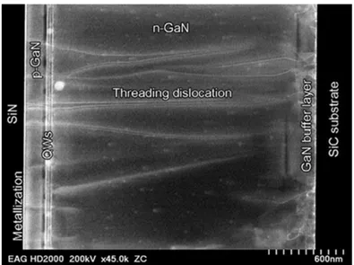
The most widespread growth technique of GaN structures is hetero-epitaxial growth by metal-organic chemical vapor deposition (MOCVD) on lattice mismatched substrates such as c-plane sapphire (α − Al2O3) and SiC (6H-SiC). To absorb strain originating during hetero-epitaxial growth, a GaN buffer layer is usually grown. Because of the large lattice mismatch (16% for GaN on sapphire and 3.5% for GaN on SiC) and different thermal expansion coefficients, threading dislocations (TD) with very large densities, typically ranging between 107 cm-2 and 1010 cm-2, are formed (Figure 5). In principle, TDs may act as non-radiative recombination sites reducing the probability of radiative recombination, and as scattering centers decreasing the mobility of free carriers. [9]
It is very surprising that with such high density of TDs GaN-based devices can still be highly efficient. Different explanations have been proposed for this. Hangleiter et al.
Figure 5 – TEM image showing threading dislocations in a GaN LED structure grown on SiC. Image from North Carolina State University, Ref. [9].
suggested that V-shaped pits nucleating on every TD form sidewall QWs with higher band gap energy that create a potential barrier around every defect and prevent the carriers from entering and recombining non-radiatively at the dislocation [10]. However, this effect seems to be a non-universal phenomenon that depends on the growth condition, as there have been reports showing that similar sidewall QWs can have lower band gap energy [11]. Another mechanism that has been proposed is carrier localization in radiative centers [12] due to random alloy fluctuations statistically occurring in nitride ternary alloys, such as InGaN. The importance of compositional disorder will be discussed in more details in Chapter 3.
There have been consistent efforts to reduce the TD density in nitrides [13]. Silicon-valley LED manufacturer Soraa was founded in 2008 by Shuji Nakamura, Steven DenBaars and James Speck based on the principle that GaN structures grown on bulk GaN substrates would ultimately outperform conventional LEDs grown on sapphire or SiC. Thanks to the developed GaN-on-GaNTM technology, Soraa LEDs have
dramatically reduced TD densities and can be operated at high current density with high efficiency [14]. Consequently, these LEDs can be 15 to 25 times smaller than conventional power LED devices leading to competitive chip prices despite the expensive bulk GaN substrate.
1.2.2 Poor conductivity of p-GaN
The elementary building block of the vast majority of semiconductor devices is the p-n junction in which different regions of the crystal structure are selectively doped with donors or acceptors. These impurities introduce reasonably shallow energy levels that lie in proximity of the conduction or valence band edge giving free carriers (electrons or holes) in the semiconductor.
Historically one of the major obstacles to the realization of nitride devices has been the growth of p-doped GaN. After initial attempts with Zn, Cd and Be the only working dopant for p-type GaN was established to be Mg. Nevertheless due to passivation by H, coming from precursors during the MOCVD growth, Mg acceptors could not be activated resulting in highly resistive layers (106 Ω ⋅ cm, Ref. [15]). In 1989 Akasaki and Amano at Nagoya University discovered that p-GaN could be activated by breaking Mg-H complexes with low-energy electron beam irradiation [16]. This method allowed to obtain a hole concentration of 2 × 1016 cm-3 which was still too low to fabricate
where he managed to activate p-GaN by means of post-growth thermal annealing above 700°C in N2 ambient obtaining a hole concentration of 3 × 1017 cm-3 [15].
Despite decades of development, today Mg-doped p-GaN is still a poor conductor due to the large activation energy EA of Mg acceptors which is ~170 meV [17]. The deep acceptor levels force to use high dopant concentrations NA in p-GaN to obtain a sufficient hole concentration for practical applications. The hole concentration p can be estimated as (Ref. [18], p. 63):
𝐩 = 𝐍𝐀
𝟏 + 𝟒 ⋅ 𝐞𝐄𝐀−𝐄𝐅/𝐤𝐁𝐓 (1)
where 𝐸𝐹 is the Fermi energy with respect to the valence band maximum (VBM) and
𝑘𝐵𝑇 is the thermal energy. Taking 𝑁𝐴 = 2 ⋅ 1020 cm-3, assuming 𝐸𝐴− 𝐸𝐹 = 118 meV
(Ref. [19], p. 39) at room temperature, 𝑝 is ~5 ⋅ 1017 cm-3, that is only 1 acceptor
among 400 is ionized. For this hole concentration, assuming a hole mobility 𝜇ℎ of 4 cm2/V⋅s (Ref. [19], p. 43) the bulk resistivity of the p-GaN layer is calculated to be
~3 Ω ⋅cm from
𝛒𝐛𝐮𝐥𝐤 = (𝐩 ⋅ 𝐞 ⋅ 𝛍𝐡)−𝟏 (2)
The most important consequence of the poor conductivity of p-GaN is that the hole current injected in the p-layer of nitride devices tends to accumulate in proximity of the p-contact without spreading uniformly in the p-layer. This effect is known as current crowding and will be further discussed in Sec. 2.5.1 and Appendix 5.2. In order to contrast current crowding, a very thin indium tin oxide (ITO) layer is usually deposited on the surface of p-GaN. ITO allows spreading current homogeneously in the p-layer because of its high conductivity (𝜌𝑏𝑢𝑙𝑘~5 ⋅ 10−4 Ω ⋅cm) while absorbing only a small
fraction of LED light thanks to its low absorption coefficient at the corresponding wavelength (𝛼𝐼𝑇𝑂~500 cm-1).
1.2.3 Compositional disorder in nitride ternary alloys
As already mentioned, by making ternary alloys between InN, GaN and AlN it is possible to span band gap energies ranging between 0.7 eV and 6.2 eV, which gives a large versatility in the design of nitride structures. Common building blocks of nitride devices are InGaN QWs and AlGaN barriers with In or Al compositions that can vary between few % to several tens of %. An intrinsic material property of ternary alloys is compositional disorder that is statistically determined. For instance, an In0.1Ga0.9N layer
has a crystal structure similar to that of pure GaN but where N atoms are held at the same positions and the other atomic sites are occupied with a probability of 10% by In atoms and 90% by Ga atoms.
Compositional disorder can be characterized by atom probe tomography (APT), a destructive microscopy technique based on time-of-flight of ions evaporated from the sample and allowing to reconstruct a 3D atomic map of the specimen. Figure 6 shows a typical In composition map measured by APT corresponding to the mid-plane of an InGaN QW of a blue LED [20]. As it can be observed for an average In composition of 15% strong compositional fluctuations occur in the plane of the QW. Two essential pieces of information can be deduced from APT measurements of nitride ternary alloys [21]:
Compositional disorder in InGaN layers is purely random, i.e. uncorrelated. APT allows to shed light on a long-lasting debate on the nature of disorder, random or correlated, in InGaN [22];
The typical length scale of compositional disorder is of few nanometers, which makes its experimental characterization challenging.
APT measurements provide atomic maps of InGaN and AlGaN layers but do not explain how the observed compositional disorder may affect the optoelectronic properties of nitride devices. To address this issue it is necessary to describe and characterize the disorder-induced fluctuations occurring in the conduction and valence band of the material that are “seen” by the free charge carriers. This problem will be tackled in Chapter 3 by means of an original theoretical approach allowing us to
Figure 6 – 2D atomic map of indium atoms in the mid-plane of an InGaN/GaN QW measured by atom probe tomography [20]. For a mean In composition of 15% large compositional fluctuations are observed.
incorporate the effect of disorder in the simulations of nitride semiconductor structures without having to solve the complicated eigenvalue problem corresponding to the Schrödinger equation of the disordered system. Moreover this approach will be validated by an experimental characterization of disorder by light absorption measurements in InGaN layers of different compositions.
1.2.4 Polarization-induced electric fields in nitrides
Electric polarization plays a key role in determining the optical and electrical properties of nitrides. A distinction has to be made between spontaneous (𝑃𝑠𝑝) and piezoelectric
(𝑃𝑝𝑧) polarizations. 𝑃𝑠𝑝 is due to the lack of inversion symmetry of the crystal structure and is strong in nitride crystals in the wurtzite phase. For instance, the spontaneous polarization constant of GaN is 0.03 C/m2 [23] giving a surface-polarization charge
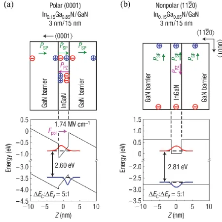
Figure 7 – Structures and simulated band diagrams of In0.15Ga0.85N/GaN QWs
grown on (a) polar and (b) nonpolar crystal orientations. The resulting polarization in the InGaN layer in (a) is dominated by the piezoelectric polarization, which determines the direction of the electric field in the QW. Reproduced after Ref. [12].
density of 2 ⋅ 1013 cm-2. 𝑃
𝑝𝑧 is induced by the strain at the interface between two layers
with different lattice constant. The piezoelectric coefficients of III-N’s are an order of magnitude larger than other III-V semiconductors, such as GaAs, GaP and GaSb.
It is of particular interest to consider polarization effects along the [0001] direction of the wurtzite crystal since conventional nitride structures are epitaxially grown on c-plane along this axis. An example of polarization effects on the optoelectronic properties of InGaN/GaN QWs grown on different crystal directions is shown in Figure 7. In the structure grown on c-plane (Figure 7a) a strong polarization-induced electric field 𝐹𝑝𝑜𝑙 is present in the QW. Typical electric field values measured in similar InGaN/GaN structures are larger than 1 MV/cm for In compositions above 10% [24]. There are three important consequences due to the strong 𝐹𝑝𝑜𝑙:
The electron and hole wave functions are spatially separated.
The QW emission energy undergoes a redshift (compare with the nonpolar structure with 𝐹𝑝𝑜𝑙 = 0 in Figure 7b). This effect is known as the
quantum-confined Stark effect (QCSE).
Increasing the carrier concentration in the QW will screen 𝐹𝑝𝑜𝑙 and cause a
blue-shift of the QW emission energy.
It is clear from these points that the description of the steady-state operation of an optoelectronic device suffering from polarization-induced electric fields in the active region will be quite complicated. In particular, it should be noted that the spatial separation of the electron and hole wave functions reduces the oscillator strength of the e-h pair thus decreasing the recombination rate and the radiative efficiency of the
Figure 8 – Schematic of an AlGaN/GaN HEMT device. The 2DEG in the GaN channel is due to the polarization discontinuity at the AlGaN/GaN interface.
structure. Much effort has been dedicated to the growth of nitride LEDs along alternative orientations [25] with reduced (semipolar) or no (nonpolar, Figure 7b) polarization along the growth direction, in order to mitigate or eliminate these polarization effects.
However it is interesting to note that polarization effects are not always detrimental to nitride devices. For instance, the 2DEG in AlGaN/GaN HEMTs is induced by the discontinuity of polarization at the heterojunction (Figure 8). Therefore, unlike AlGaAs/GaAs HEMTs in which intentional modulation doping is required to create charges in the channel, polarization can be used in nitrides as a tool to design the 2DEG carrier density as a function of the thickness and composition of the AlxGa1-xN
barrier [26]. Note that the penetration of the wave function into the AlxGa1-xN barrier
causes scattering by random alloy disorder limiting the mobility of the 2DEG. This issue can be attenuated by the growth of a thin AlN layer at the interface confining the 2DEG in the channel.
1.3 Efficiency droop in nitride LEDs
LED efficiency droop is a complex problem in III-nitrides as it involves, among others, all the issues already discussed in this chapter. For this reason, it is one of the most debated topics in the LED community. An illustration of the droop phenomenon is given in Figure 9. In presence of droop, the optical output power of a nitride-based LED increases sublinearly with the injected current density (inset). The corresponding efficiency curve of the LED is represented by the continuous red line. The peak efficiency of the device occurs at low current density, while at higher injection the LED efficiency “droops”. The most important consequence of droop is that currently LED bulbs are made of several LED chips allowing to operate each device at its peak efficiency and still obtaining a sufficient total luminous flux from the bulb, but at the expense of a much higher cost of the lamp. Understanding and solving the droop problem represents a major challenge in view of the application of LEDs to solid-state lighting as the requirement in terms of energy saving is to at least displace the quite efficient fluorescent, sodium, and high intensity discharge lamps used today in the main energy consuming lighting sectors, industrial, commercial and outdoors, with more
Figure 9 – Illustration of the effect of droop in a simulated nitride-based LED from Ref. [27]. In presence of droop, the LED efficiency curve (red curve) decreases at high current density, while the ideal trend calculated without droop (green curve) approaches the unity efficiency. The inset shows the corresponding optical powers of the LED exhibiting a sublinear increase with current density in the case of droop, and a linear dependence without droop.
efficient and better light quality lamps. To achieve this, LEDs have to perform at the physical limits of electricity-to-light conversion efficiency, requiring mastering of the intrinsic electrical and optical properties of the materials, and of the electromagnetic properties of the device structure. The goal is to obtain single-chip LED bulbs that are highly efficient at high current density (“no droop” limit shown as a green curve in Figure 9) and at the same time cost-competitive with the other commercial light sources. [27]
The conversion efficacy of electricity into white light in LEDs (𝜂𝐿𝐸𝐷, lumens out/electrical power in) is mainly the product of five terms:
𝛈𝐋𝐄𝐃 = 𝛈𝐞𝐥× 𝛈𝐢𝐧𝐣× 𝐈𝐐𝐄 × 𝛈𝐞𝐱𝐭× 𝐋𝐄𝐑 (3)
𝜂𝑒𝑙, the electrical efficiency, mainly associated with ohmic or contact losses (mostly related to p-GaN, as discussed in Sec. 1.2.2), which represents the fraction of electrical power not injected as e-h pairs;
𝜂𝑖𝑛𝑗, the injection efficiency which describes the fraction of current injected into the light-emitting region;
IQE, the internal quantum efficiency which describes the conversion of injected electron-hole pairs into photons inside the active part of the LED structure; 𝜂𝑒𝑥𝑡, the light extraction efficiency which gives the fraction of photons emitted
outside the LED to those generated inside;
𝐿𝐸𝑅, the luminous efficacy of radiation of the emitted light (lm/W), which represents its visual efficiency, characteristic of the emitted spectrum, and is connected to the color rendering of the light source. A source at the peak of eye sensitivity (555 nm) yields by definition 683 lm/W, but is not white. Adding red and blue to the spectrum reduces lm/W. Depending on the technology used to generate white and on color quality, for instance as displayed by the CRI, the maximum LER is in the 300–400 lm/W range [28,29].
The product of the 3 middle terms gives the external quantum efficiency (EQE).
Much effort has been made to optimize the LED efficiency. In the first place the problem of light extraction was tackled. In principle only a small fraction of the light that is generated in a nitride LED can be directly extracted from the device. The reason for this is that the refractive index of AlInGaN compounds has a typical value of 2.4-2.5 which is often larger than those of the media surrounding the LED. For instance, in the
within a narrow cone defined by 𝜃𝑐 = 𝑠𝑖𝑛−1(𝑛
𝑒𝑥𝑡/𝑛𝑖𝑛𝑡) is directly extracted (Figure
10a). The rest of the light is trapped as a guided mode in the semiconductor by total internal reflection and would usually end up being reabsorbed, dissipating its energy into heat.
In order to increase 𝜃𝑐, LEDs are often encapsulated in hemispherical epoxy or silicone
domes (see Figure 3a) with a refractive index of ~1.5, closer to the refractive index of the semiconductor than 𝑛𝑎𝑖𝑟. (UV LEDs are an exception. No epoxy or silicone dome is used in this case as this would cause strong optical absorption losses in the UV range.) Thanks to the geometry of the dome light rays extracted into the epoxy impinge at the surface almost perpendicularly and are transmitted into air.
In addition to this, various texturing techniques have been developed to improve light extraction from LEDs (Figure 10b-e). The two main approaches are surface roughening [30] and substrate patterning [31] aiming at randomizing the trajectory of trapped light. After some random propagation within the LED, the beam, if not absorbed, will strike the interface within the extraction cone. Side shaping [32] can lead to sizeable low loss side extraction when using transparent index-matched substrates. A light extraction method relying on wave optics rather than geometrical optics is based
Figure 10 – (a) Diagram showing different possible paths for light propagation in a planar luminescent semiconductor slab embedded between a substrate and air. Only the light propagating within the air and substrate extraction cones may be directly extracted from the semiconductor. Adapted from Ref. [33]. (b)-(e) Various techniques of light extraction features for LEDs: (b) surface roughening [30]; (c) substrate patterning [34]; (d) side shaping [14]; (e) photonic crystal [35]. nint next,1 next,2 Guided light Extracted light Extracted light (c) (d) (e) (b) 500 nm 200 nm (a)
on photonic crystals [33]. The main advantage is emission directionality, which does not seem yet a large enough advantage to offset the demanding fabrication technology. These techniques have led to a remarkable progress in the past decade increasing the light extraction efficiency in nitride LEDs from roughly 20% to over 85%. [34,35]
The technological solutions developed in the last decade have led to remarkable progress in all components of the efficiency allowing to attain EQE’s of 80+% in blue LEDs at peak efficiency [36], corresponding to low current densities of the order of 1-10 A/cm2. However getting nearer the physical limits could lead to increasing by 60% the performance of LEDs in the market: the product of several efficiency factors in the 80+% range leads to today’s overall efficiencies around 39% for warm-white phosphor-converted LEDs, with a 2020 target of 62% (Ref. [29] p. 34). Moreover, as already mentioned, solving the problem of LED droop by extending the high-efficiency performances to high current densities would allow decreasing the chip area and reduce the cost of the devices on the market.
Different non-radiative losses, specifically related to microscopic electronic processes occurring in the active region of the LED, may affect the efficiency of the 𝜂𝑖𝑛𝑗 and IQE terms appearing in Eq. (3) and cause droop (Figure 11). The main proposed droop mechanisms affecting 𝜂𝑖𝑛𝑗 (Sec. 1.3.1) and IQE (Sec. 1.3.2) will now be presented. Then the problem of the identification of the dominant mechanism for droop will be discussed (Sec. 1.3.3). Finally, remedial action for diminishing droop will be briefly reviewed (Sec. 1.3.4).
Figure 11 – Principle of different non-radiative microscopic electronic processes which have been proposed to explain droop: (a) carrier overflow; (b) defect recombination following band filling of localized states; (c) direct and phonon-mediated e-e-h Auger recombination.