OATAO is an open access repository that collects the work of Toulouse
researchers and makes it freely available over the web where possible
Any correspondence concerning this service should be sent
to the repository administrator: [email protected]
This is an author’s version published in:
http://oatao.univ-toulouse.fr/24481
To cite this version:
Guerch, Kévin
and Dekany, Justin and Dennison, John Robert and
Christensen, Justin and Paulmier, Thierry and Guillemet, Sophie
and
Lenormand, Pascal
Cathodoluminescence studies of defects in coated
boron nitride. (2017) Journal of Physics D: Applied Physics, 50 (29).
295302. ISSN 0022-3727
https:l/doi.org/10.1088/1361-6463/aa78b7
Cathodoluminescence studies of defects in
coated boron nitride
Kévin Guerch1 •2•3, Justin Dekany2, J R Dennison2, Justin Christensen2, Thierry Paulmier1 , Sophie Guillemet-Fritsch3 and Pascal Lenormand3
1 ONERA, 2 venue Edouard Belin 31055 Toulouse Cedex 4, France
2 Materials Physics Group, Physics Department, Utah State University, Logan, UT 84322, United States of America
3 CIRIMAT, Université de Toulouse, CNRS, UPS, 118 route de Narbonne 31062 Toulouse Cedex 09, France
E-mail: [email protected] and [email protected]
Abstract
Optical emission properties of boron nitride (BN) substrates, BN with alumina (A!iO3)
coating, and thermally-annealed alumina-coated boron nitride (an-BN/A!iO3) were
investigated under electron irradiation using cathodoluminescence (CL) measurements.
Tests were performed, temperatures ranging from -lO0K to -300 K, with monoenergetic beams from 5 keV to 30keV, and electron flux densities from I nA • cm-2 to 500 nA • cm-2. These experiments were conducted to identify the effects of coating and thermal annealing on the nature and occupation of defect states in different samples with BN substrates. Previous studies have shown that these treatments can limit the charging of BN substrates. Consequently, thorough investigations of electron trapping and recombination processes as a fonction of low temperature, dose and charging/discharge were performed in order to explain the differences of electrical behaviour and compare the CL spectra of the three different samples studied. Broad features associated with the BN and sharper features resulting from the annealed alumina coating were observed. Changes in the intensity, energy, and width of the features with sample lreatments were observed. Different incident beam parameters were used to associate these features with specific types of defect states. The effects of charging, temperature- and dose-dependent conductivity, and thermal annealing and aging of the samples on the CL spectra were investigated. These were used to study defect creation and occupation and to understand the predominant physical mechanisms and main structural and chemical differences between these ceramic configurations.
Keywords: aluminum oxide, boron nitride, cathodoluminescence, charging, coating, defects, electron irradiation
(Sorne figures may appear in colour only in the online journal) 1. Introduction
Technical ceramic materials are subjected to extreme condi tions in plasma environments, such as those encountered by satellites in space [I], devices for plasma vapour deposition [2], high power applications [3], or nuclear radiation [4]. To survive, these ceramic insulators must have exceptional elec trical and thermal properties. Boron nitride (BN) is used in
particular because it combines good electrical insulation and high thermal conductivity [5]. However, partially shielded environments such as those found in spacecraft interiors irra diated by electrons with preferentially higher energies can lead to charge trapping in the ceramic's bulk. With the aim to limit charging of BN under electron irradiation, studies of a coating and a thermal treatment of this substrate were per formed. Specifically, BN subslrates were coated with alumina
(Al2O3) coatings (using plasma vapour deposition) with some
coated BN subsequently subjected to thermal annealing under vacuum.
This study focuses on the nature, density and occupation of the localised defects (traps), which control electrical and optical behaviour in these systems. These traps are generated from physical (e.g. vacancies, interstitial, or grain bounda-ries) and chemical (e.g. substitutional or interstitial impuri-ties) defects in the crystallographic phase of materials. Trap depths (i.e. the binding energies of trapped charges) depend on the nature of the defects. Simple band theory of disordered materials, based on the energy and spatial distributions of these deep trap (DT) defect states, is used to describe the dark conductivity and radiation induced conductivity (RIC) [6] and the electron beam-induced optical emission (cathodolumines-cence) spectra.
On one hand, we compare the nature and densities of defects of BN substrates, alumina-coated BN (BN/Al2O3),
and annealed Al2O3-coated BN (an-BN/Al2O3) through
studies of the energies and intensities of spectral features of emitted light. On the other hand, we investigate the sig-nificant influence of thermal annealing and extended radia-tion doses (aging) experienced by the materials on charge trapping processes, trap creation and annihilation, electron release kinetics, and charge mobility. The sample temper-ature during irradiation tests has a substantial influence on electron transport and optical spectra through the electron transitions in the band gap of an-BN/Al2O3. These, in turn,
are related to the charging/discharge processes and espe-cially to the sample surface deterioration as a function of time and thus of dose.
2. Experimentation
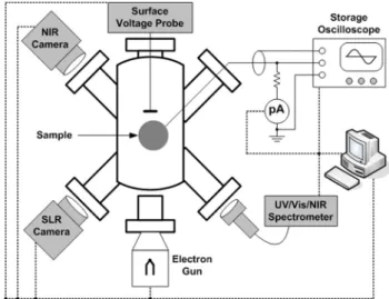
The ultrahigh vacuum electron emission test (EET) chamber at Utah State University [7, 8] was used to investigate the cathodoluminescence (CL) of the ceramic samples. Figure 1 provides a schematic overview of instrumentation used during the tests described herein. This versatile facility allows the
characterization of spacecraft materials in different repre-sentative space conditions. Ultrahigh vacuum (~1.10–6 Pa) is achieved through use of mechanical, turbomolecular and ion pumps. For most tests, samples were mounted on a carousel held at room temperature which has ten sample holder faces and one location for a Faraday cup used to monitor incident beam profiles and fluxes. Low temperature tests from ~100 K up to ~300 K were made using a cryogenic sample holder [9], using a closed-cycle He refrigerator installed on a flange of the chamber. A high-energy electron gun (Kimball, Model EGPS-21B) provided an electron beam with incident ener-gies of 5 keV to 30 keV (5, 10, 15, 20, 25 and 30 keV ±0.1% during tests). Stable and reproducible incident electron fluxes of 1 nA · cm−2 to 500 nA · cm−2 (1, 10, 30, 100, 500 nA · cm−2
±3% during tests) with a beam diameter of ~1 cm2 FWHM
were used [10].
The visible/near infrared (Vis/NIR) emission from samples under electron irradiation was measured with two cameras and a spectrometer [9]. Colours and intensity of glow were cap-tured with a single-lens reflex (SLR) CCD camera (Cannon, EOS Rebel XT DS126071; ~400 nm–700 nm in RGB format, capture time of 1 s/frame, with an average spectral response of ~4 · 109 counts/(W cm−2· sr · µm)). The low intensity of light
was monitored with a Vis/NIR image-intensified video camera (Xybion, ISG-780-U-3; ~400 nm–900 nm, 30 frames s−1,
with an average spectral response of ~4 · 1010 counts/(W cm−2
· sr · µm)). The absolute sensitivity of the cameras were cali-brated against National Institute of Standards and Technology (NIST) traceable sources. A UV/Vis fibre optic spectrometer (Stellarnet, 13LK-C-SR; ~350 nm–1080 nm with 0.5 nm or 2 meV resolution) was used to measure the luminescence emission spectra [1].
The materials studied are industrial samples (~1 × 1 × 10 mm) of pyrolytic hexagonal boron nitride (BN), alumina-coated boron nitride (BN/Al2O3), and annealed
alumina-coated boron nitride (an-BN/Al2O3). Commercial
BN was coated with alumina (~0.3 µm thickness) using an
industrial PVD-RF method. The industrial thermal annealing treatment was carried out under vacuum. Surface roughness was equal to ~0.5 µm prior to coating [12]. Before irradia-tion tests, samples were cleaned with methanol and under-went a 48 h vacuum bakeout at ~375 K and <1.10–3 Pa in
order to eliminate adsorbed water and volatile contaminates. Subsequently, they were installed in EET chamber at low pres-sure (<1.10–6 Pa) for a duration higher than 30 hours to allow
outgassing prior to irradiation tests. Samples for room temper-ature tests were mounted on grounded Cu sample holders on the EET sample carousel. Several samples of an-BN/Al2O3
were mounted side-by-side on a similar grounded Cu sample holder attached to the cryostat in order to increase the exposed sample surface area for temperature-dependent tests.
Accurate prediction of luminescence intensity from multi-layered materials is difficult, especially for materials with different densities, thicknesses, atomic weights, backscatter coefficients and scattering cross-sections [13]. Production of cathodoluminescence results from the deposition of inci-dent electron energy and creation of electron-hole pairs in the material. The energy and depth dependence can be modelled
Figure 1. Diagram of instrumentation used to characterise samples
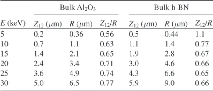
through complex Monte Carlo simulations such as CASINO [14], or can be characterized by a single parameter such as the electron penetration depth or the range [15] in the continuous slow down approximation (CSDA) [16, 17]. Table 1 compares values of the penetration depth (depth at peak energy loss) from CASINO simulations to range in the CSDA for bulk Al2O3
and BN over the experimental energies. These two measures for energy deposition are consistent with one another, based on a relation developed by Bentabet [18, 19]. In a spherical geometric model for a semi-infinite target, Bentabet shows the mean penetration depth Z12=( / )(R2 1−η)
( )
1−σσTrel . The
term with the backscatter coefficient η corrects for
backscat-tered electrons and the term involving the transport cross- section σTr and the elastic cross-section σel corrects for inclu-sion of elastic scatter; both terms are weakly energy dependent with (1−η) increasing with increasing energy and (1−σσTr)
el
decreasing such that Z12≈0.45⋅R for both materials over the
experimental energy range. The CASINO results for h-BN are in fair agreement with limited experimental data [20]. The asymptotic limits of η at high energies were measured
for bulk microcrystalline Al2O3 and h-BN to be 0.2 and 0.15,
respectively.
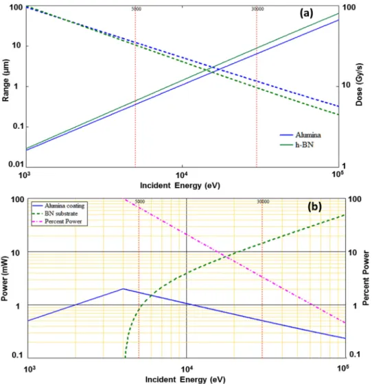
A simple model for luminescence production in the Al2O3
coating and BN substrate appropriate for the course data presented here follows from a calculation of the electron range (CSDA), R(Einc), as a function of incident energy, Einc
(figure 2(a)) assuming bulk densities ρm of 3.45 g · cm−3 for
BN and 3.97 g · cm−3 for Al
2O3 [16]. The range of hexagonal
sp2-coordinated BN has been approximated using an
esti-mated effective number of valence electrons NVeff = 2.742.
NVeff is predicted from a simple formula—involving band gap energy (~6 eV for hexagonal BN [20, 21]) plus the average atomic weight and atomic number—which was determined by fitting NIST range data in the CSDA [17] and NIST ine-lastic mean free path data [22] for a wide range of materials [23]. Figure 2(a) also shows the energy-dependent dose rate
( ) (= )/[ ( ) ]ρ
D E˙ inc J Einc inc q R Ee inc m for a 500 nA · cm−2 non-penetrating beam in the CSDA [8]. Figure 2(b) shows the mean power density deposited by a beam of area A and range
R(Einc)—which is given as P E A( )/ =(J Einc inc)/qe—in the ~300 nm thick alumina coating and the underlying BN substrate of BN/Al2O3 and an-BN/Al2O3 samples for a 500 nA · cm−2
beam. Note that at the lowest incident energy, the electron beam just penetrates the estimated thickness of the Al2O3
coating. Since electron range increases with beam energy, the
dose imparted to the fully penetrated Al2O3 coating (or
simi-larly, to a thin surface layer of BN) decreases with increasing incident energy from ~75% at 5 keV to ~4% at 30 keV (figure 2(b)). Use of the penetration depth for this analysis would shift the power deposition curve to higher energies by about 35%; however, penetration depth and range scale with density, so values in figure 2 are overestimated for less dense coatings and rough surfaces.
3. Results and discussion
3.1. Results for BN and BN/Al2O3
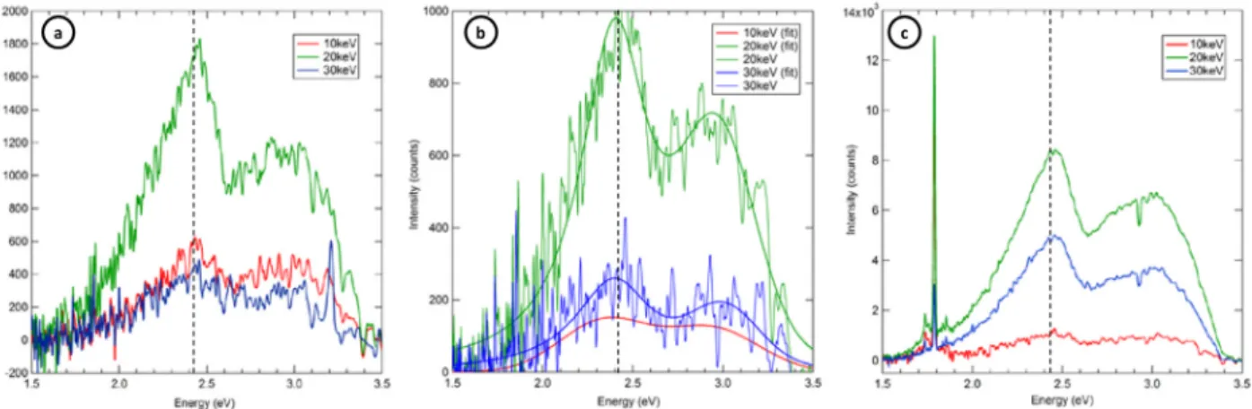
Emission spectra as a function of photon energy and wave-length are shown in figure 3 for an uncoated BN sample irradi-ated with 5 keV and 30 keV electrons. The red curves represent the emission spectra raw data; the small intensity of lumines-cence from BN substrates results in a low signal-to-noise ratio (SNR). These spectra were fitted with least-squares methods for up to four Gaussian peaks with peak central energy, width, and amplitude as fitting parameters. The black curves show the sum of the individual fitted peak profiles and component curves are shown below.
The intensities of BN/Al2O3 spectra have consistently even
lower SNR than those of BN. Hence, for clarity sake, the composite fit emission spectra of BN/Al2O3 at various
inci-dent electron energies are shown in figure 4(b), while only raw data are shown for BN. Since the observed features were broad, such smoothing is acceptable. Gaussian peak profiles were found to produce better fits than Lorentzian or Voight functions, as would be expected for long-lived deep level trap states (see below) with very little lifetime broadening [8]. Gaussian widths are a reasonable measure of the DT energy density of states widths, since measured widths are much larger than the 2 meV instrumental resolution.
For the BN substrate (figure 3), two broad peaks were observed at ~2.4 eV (~516 nm) and ~3.0 eV (~416 nm). Cathodoluminescence spectral features of BN have been dif-ficult to identify and associate with specific defect structures due to the different band gap energies (~4.5 eV to ~6.5 eV) [20] and structures associated with cubic (sp3-bonded) c-BN
[24, 25], hexagonal (sp2-bonded) h-BN [20, 24, 26], boron
nitride nanotubes [24], and disordered BN such as pyrolytic pBN [24]. Broad peaks at 2.48 eV (attributed to multiva-cancy complexes of B and N vacancies in c-BN) and 3.12 eV (of unknown origin) have been reported in CL spectra of higher purity c-BN close to our observed peaks at ~2.4 eV and ~3.0 eV. However, sharper peaks of similar intensities at 2.81 eV, 3.01 eV and 3.20 eV attributed to c-BN and a broad intense peak at ~3.55 eV attributed to h-BN seen in [25] were not observed in our spectra.
The intensities of BN/Al2O3 spectra are lower than those
of BN. The integrated peak intensities at given incident ener-gies of both of the two observed broad ~2.40 eV (figure 5(a)) and ~2.98 eV (figure 5(b)) peaks for the BN/Al2O3 spectra are
consistently ~50% smaller than corresponding peaks for BN. However, the shapes of the ~2.40 eV and ~2.98 eV peaks— indeed the shape of the full spectra from 1.5 eV to 4.5 eV—are
Table 1. Penetration depth and range of Al2O3 and h-BN.
Bulk Al2O3 Bulk h-BN E (keV) Z12 (µm) R (µm) Z12/R Z12 (µm) R (µm) Z12/R 5 0.2 0.36 0.56 0.5 0.44 1.1 10 0.7 1.1 0.63 1.1 1.4 0.77 15 1.4 2.1 0.65 1.9 2.8 0.67 20 2.4 3.4 0.71 3.0 4.6 0.66 25 3.6 4.9 0.74 4.3 6.6 0.65 30 5.0 6.5 0.77 5.9 9.0 0.66
Figure 3. Emission spectra of BN at room temperature with a 500 nA · cm−2 incident beam at (a) 5 keV and (b) 30 keV. Lower graphs show
the component curves in the fits.
Figure 2. (a) Range (solid curves, left axis) and dose for non-penetrating beam (dashed curves, right axis) as a function of incident energy.
(b) Power deposited (left axis) in 0.3 µm Al2O3 coating (solid curve) and BN substrate (dashed curve) as a function of incident energy for a
500 nA · cm−2 beam. Percentage of incident electron power absorbed in Al
2O3 coating (right axis, dash-dotted curve). The 5 keV to 30 keV
very similar for the BN and BN/Al2O3 spectra (figure 4).
The peak energies of the two observed broad ~2.40 eV and ~2.98 eV peaks for BN/Al2O3 spectra coincide with those of
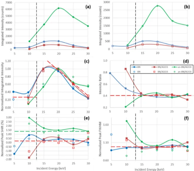
the BN spectra to within <0.5% above 10 keV incident ener-gies and deviate at lower enerener-gies by <1.5% (figure 5(e)); numerical uncertainty due to the fitting process is 1%. The peak widths for both peaks show little change from the mean high energy peak FWHM of 0.49 ± 0.04 eV over the full incident energy range and are similar for both BN and BN/Al2O3 (figure 5(f)). The ratios of intensities of ~3.0 eV
peak to ~2.4 eV peak at the same incident energy (I2.98/I2.40) for
both BN and BN/Al2O3 has a mean ratio of 0.41 with average
deviation of <2% above 10 keV incident energies, though the ratios do increase substantially at lower energies (figure 5(e)). The fact that the addition of a coating does not change the broad shape of the spectra and produces no new sharp spec-tral features—as are seen for an-BN/Al2O3 (see below)—
suggests that the as-deposited PVD-RF Al2O3 coating of
BN/Al2O3 does not have appreciable cathodoluminescent
active or absorptive states in the 1.5 eV–4.5 eV range. Rather, the Al2O3 coating acts to absorb about half of the power from
incident electrons, thereby reducing the dose to BN and the resulting BN emission intensity as the incident beam is attenu-ated passing through the Al2O3 coating.
Additional information about the power deposition can be deduced from the relative changes in emission intensity as a function of incident electron energy. Given the conclusion above, that the unannealed Al2O3 coating does not contribute
appreciably to the emission spectra, these energy dependent changes most likely result from difference in the rough sur-face layer and bulk of the BN substrate. Such sursur-face state effects could result from the mechanical treatment of the BN surface which produces a local mechanical strain or from the significant surface roughness. There is a surprisingly con-sistent dependence on incident energy for both the ~2.98 eV and ~2.4 eV peaks of both BN and BN/Al2O3 samples. Both
peaks for both materials show a distinctly different behav-iour in relative intensity (figures 5(c) and (d)), peak position (figure 5(e)), and (to a lesser extent) peak width (figure 5(f)) at lower incident energy electrons below 15 keV (which are more surface sensitive due to reduced electron penetration (see
figure 2(b))). Figure 5(c) shows the relative change of the inte-grated intensity of the ~3.0 eV and ~2.4 eV peaks for both BN and BN/Al2O3 (i.e. the integrated peak intensities nor malized
to largest intensity for each peak of each sample), plotted as a function of incident energy. The horizontal dashed red line indicates mean low energy behavior at <15 keV, ~30% of the maximum normalized intensities for each peak and sample near 20 keV. The sloped dashed red line (in figure 5(c)) is a linear fit to decreasing intensity above 15 keV, with a decrease of 76% from 20 keV to 30 keV. A similar decrease of 50% is predicted for the fraction of power deposited in a 0.3 µm
surface layer from 20 keV to 30 keV (figure 2(b)). Both the BN ~2.40 eV and BN ~2.98 eV peaks in both the BN and BN/Al2O3 spectra show a ~40 meV (~1.5%) shift to lower
ener-gies (see figure 5(e)) at incident electrons energies <15 keV. This suggests that at lower incident energies (where a higher faction of the incident power is deposited in the surface layer), BN surface DT states are more weakly bound than the bulk DT states. Substantial decreases in integrated peak intensi-ties for the ~2.40 eV and ~2.98 eV in both BN and BN/Al2O3
spectra are likewise observed at lower incident energies (figures 5(a) and (b)). Further, the relative density of deeper traps to shallower traps—as reflected in the ratio of peak inten-sities (I2.98/I2.40) (figure 5(d))—increases below 15 keV for both
BN and BN/Al2O3 samples, with BN/Al2O3 exhibiting a larger
change than BN; this could indicate that the relative fraction of surface states is larger for BN/Al2O3 than for BN samples and
for the ~2.98 eV defect than for the ~2.40 eV defect. 3.2. Results for an-BN/Al2O3
Emission spectra of an-BN/Al2O3 for several incident electron
energies are dramatically different than BN and BN/Al2O3
spectra. Overall, CL intensity from an-BN/Al2O3 is
sub-stantially higher, with higher SNR; consequently, the curves shown in figure 4(c) are raw data rather than fitted curves.
First, we consider the broad peaks at ~2.40 eV and ~2.98 eV which we previously attributed to the BN substrate. The CL intensities of these two peaks at 20 keV when the peak inten-sity is highest are ~4–6 times more intense than the corre-sponding BN peaks and 8–12 times more intense than those
Figure 4. Emission spectra of (a) BN, (b) BN/Al2O3 and (c) an-BN/Al2O3 acquired at 500 nA · cm−2 beam current, 10, 20 and 30 keV
of unannealed BN/Al2O3 (figures 4(a) and (b)). The increase
in an-BN/Al2O3 integrated peak intensities is only about twice
that of BN at 10 keV, but increases with increasing incident energies to about 10 times at 30 keV (figures 5(a) and (b)). These increased enhancements for more penetrating higher energies suggest that they originate preferentially from deeper BN material. It was suggested in a companion study—which included measurements of Raman spectroscopy, XPS, elec-trical conductivity, and electron-induced surface charging and relaxation—that the annealing treatment of an-BN/Al2O3
generated a higher density of physical and chemical defects especially near the surface [27]. Thermal annealing could allow either chemical or physical defects inherent in the sur-face layers to diffuse further into the bulk. An alternate cause of the observed increased emissions from BN could be due to reduced surface charging from the incident electron beam.
The reduced charging could result from increased total elec-tron emission [28], as well as from increased conductivity which increased charge dissipation. Measurements showed the bulk conductivity of an-BN/Al2O3 was 15 times that of
BN and 40 times that of unannealed BN/Al2O3 [27]. Negative
surface potential of up to 3500 V was measured for BN irradi-ated with a 11 keV beam; this was reduced to ~1700 V for BN/ Al2O3 and ~200 V for an-BN/Al2O3 [27]. Enhanced negative
surface charging reduces the landing energies of incident elec-trons, thereby reducing the absorbed power and the penetra-tion range and hence reducing the CL intensity [7].
There are some small differences in the shape of these broad peaks at ~2.40 eV and ~2.98 eV. The ~2.40 eV and ~2.98 eV peak energies of an-BN/Al2O3 at incident energies >10 keV
are about 1.5% higher than those for BN and BN/Al2O3
spectra and increase modestly at lower energies instead of
Figure 5. BN cathodoluminescence peak fitting parameters as a function of incident electron energy for ~2.4 eV (filled) and ~2.98 eV
(open) peaks at 500 nA · cm−2 beam current for the three samples BN (circle), BN/Al
2O3 (square) and an-BN/Al2O3 (triangle). Vertical
dashed black lines indicate the boundary between low energy peak behavior and high energy peak behavior between 10 keV and 15 keV. (a) and (b) Integrated peak intensities, for ~2.4 eV and ~2.98 eV peaks, respectively. (c) Integrated peak intensities normalized to largest intensity for each peak of each sample. The horizontal dashed red line indicates mean low energy behavior. The sloped dashed red line is a linear fit to decreasing intensity above 15 keV, with a slope of −76%/10 keV. (d) Ratio of intensities of ~2.98 eV peak to ~2.4 eV peak (I2.98/I2.40), with 0.41 mean ratio at high energies (horizontal dashed red line). (e) Percent shift in peak energy normalized to the mean low
energy unannealed peak positions at 2.388 ± 0.005 eV (solid) and 2.995 ± 0.005 eV (open), respectively. The an-BN/Al2O3 (triangle) peaks
decreasing as for BN and BN/Al2O3 peaks (figure 5(d)).
The widths of these two peaks are similar for all three mat-erials, with some differences below 15 keV (figure 5(f)). The relative density of deeper traps to shallower traps— as reflected in the ratio of peak intensities (I2.98/I2.40)
(figure 5(d))—are nearly identical for all three samples above 10 keV, although the ratio does decrease for an-BN/Al2O3
below 15 keV. The energy dependences of the normalized integrated intensities exhibit very similar energy dependen-cies for all three materials (figure 5(c)). Altogether, these dif-ferences in spectral shape suggest the added intensity in the broad an-BN/Al2O3 spectra is not from the Al2O3 coating,
though we cannot rule out some contributions due to broad CL peaks in similar energy ranges of 3.5 eV–5.0 eV some-times observed for Al2O3 materials [29, 30].
Second, we consider additional sharp features in figure 4(c). These include a strong sharp emission peak at ~1.785 eV with numerous small sharp satellite peaks visible in figure 6, plus a sharp absorption peak at ~2.93 eV. Annealing induces both chemical and structural changes in the Al2O3, leading to CL
which can be clearly attributed to the annealed Al2O3 surface
layer. Chemical characterization of an-BN/Al2O3 with Raman
[27] and XPS [12] methods found evidence for (Cr3+)
impu-rities and chemical bonds of compounds Al(2p) and O(1s). O vacancies are known to be produced in Al2O3 in a reducing
(vacuum) environment [30] and by electron irradiation [31]; these have been associated with luminescence attributed to one electron (F+ emission) or two electron (F emission)
trap-ping processes [30].
The most prominent feature attributed to the alumina layer in figure 4(c) is a sharp and intense low energy peak at ~1.785 eV. This peak is called the ‘ruby peak’ because it is
characteristic of ruby (crystalline Al2O3 (sapphire) of the
min-eral family of corundum with Cr impurities). This peak cor-responds to the no-phonon line caused by localized chemical defects (colour centres) related to Cr3+ impurities [4, 27, 30,
32, 33]. Very low concentrations of <5 ppm of Cr3+ can cause
intense emissions [34].
Around this intense no-phonon peak at ~1.785 eV, sym-metric peaks were observed at ~1.758 eV and ~1.835 eV (figure 6) corresponding to vibrational (phonon-) assisted electron transitions, similar to those seen in previous studies [4, 27, 32]. Indeed six or more smaller satellite peaks are evi-dent in figure 6, evenly spaced at 14 ± 1 meV intervals, at energies both above and below the 1.785 eV peak. This incre-mental energy is the phonon energy. Additional satellite peaks are observed at ~1.737 eV and 1.853 eV; peaks at these ener-gies have been previously attributed to point defects of Fe2+
and Ti4+ in Al
2O3 [30].
A narrow absorption peak is observed at ~2.93 eV, super-imposed on the emission from the ~2.98 eV BN peak. Charge carriers are excited from deep traps (DT) to shallow traps (ST) in the annealed alumina coating by absorption of pho-tons coming from the luminescence of BN substrate. Carriers excited to these ST states can then be thermally excited into conducting states, thereby activating charge transport in the Al2O3 layer. This absorption band is near a band observed at
~2.89 eV from radiation induced defects [35].
All these chemical defects generating low energy electron transitions are activated by thermal annealing of the alumina coating. Consequently, the annealing process must generate several kinds of relatively low energy localized defects with substantial densities within the Al2O3 band gap. These low
energy trap states can potentially act to increase conductivity
Figure 6. Emission spectra of an-BN/Al2O3 near the 1.785 eV ruby
peak acquired at 500 nA · cm−2 beam current, 10,15, 20, 25 and
30 keV beam energies, and room temperature. Larger satellite peaks are observed at ~1.737 eV, ~1.758 eV, ~1.835 eV and ~1.853 eV are indicated by vertical dashed lines.
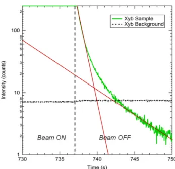
Figure 7. Delayed luminescence of an-BN/Al2O3. The electron
beam (30 keV at 500 nA · cm−2) incident on a room temperature
sample is turned off at 737 s, as denoted by the vertical dashed line. The CL intensity measured with the Xybion CCD camera (green solid line) has had the background (black curve) subtracted; the camera is saturated when the beam is on. Red lines are exponential decay fits with decay constants of 0.81 ± 0.01 s and 5.4 ± 0.1 s.
in the alumina layer in several ways. Absorption of higher energy photons from the BN luminescence could excite electrons from the low energy Al2O3 chemical defect states
directly into the CB or into ST states which are then thermally excited into the CB. Further, more mobile charge carriers in the annealed sample would reach recombination centres more easily thereby enhancing electron-hole recombination. This in turn may act to limit charging in the annealed alumina layer as compared to the unannealed alumina layer or the BN surface layer, thereby increasing the incident electrons flux reaching the BN and enhancing BN CL intensities in the an-BN/Al2O3
samples.
The glow intensity of an-BN/Al2O3 after the end of
irradia-tion is shown in figure 7. During this relaxairradia-tion phase after the beam is turned off, delayed luminescence (phosphorescence) is observed with an exponential decrease in intensity with two discernible decay constants of 0.81 ± 0.01 s and 5.4 ± 0.1 s. This delayed luminescence is characteristic of recombination processes of charges carriers after irradiation that involves detrapping of longer-lifetime trap states at the beginning of the relaxation phase.
3.3. Influence of temperature
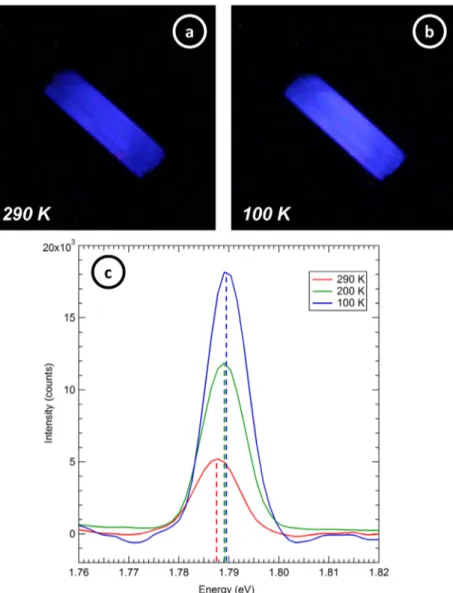
A thorough study of an-BN/Al2O3 at various temperatures
was performed in order to get more information about elec-tron transitions within the band gap of the annealed coating. Figure 8 shows the temperature evolution of the strong CL ‘ruby’ peak (related to Cr3+ defects) from an-BN/Al
2O3
exposed to an electron beam with energy of 5 keV and flux of 500 nA · cm−2. This low incident energy was chosen for three
main reasons: (i) at this energy with a electron penetration range is ~0.25 µm (figure 2(a)), most electrons were depos-ited in the ~0.3 µm thick alumina coating, thereby optimising
the CL intensity from the annealed Al2O3 layer; (ii) to limit
charging of the ceramic sample, thereby avoiding a decrease in the local incident energy which would affect CL measure-ments as a function of time and (iii) lower incident energies above the second crossover energies such as 5 keV have total electron yields near unity that cause less charging.
The overall CL intensity increases when the temperature decreases and the luminescence hue is more magenta than violet especially at the center of specimen (figure 8). That is due to a larger increase of the ‘ruby’ peak intensity than that of
Figure 8. Evolution of cathodoluminescence of an-BN/Al2O3 as a function of temperature under electron bombardment at 5 keV and
500 nA · cm−2. (a) and (b) Intensity evolution captured through SLR CCD camera photographs. (c) Temperature variation of ‘ruby’ peak
the higher energy broad peaks attributed to the BN substrate. Powell [32, 36] and Green [33] performed detailed studies of the temperature dependence of the ‘ruby’ peak (~1.785 eV). Green showed that the conversion efficiency (which is directly proportional to CL intensity) is linearly proportional to the optical phonon density which increases exponentially at lower temperatures as an Arrhenius function; his theoretical predic-tion of a ~20 increase in CL intensity from room temper-ature to 100 K is larger than the four-fold increase shown in figure 8(c).
This increase in the intensity of ‘ruby’ peak is due to a relative increase of electron transitions to the more shallow (low energy) DT states (emission from Cr3+-center: transition 2E → 4A
2 [37]). Indeed, when T decreases the deeper traps (blue and violet BN traps) become more filled because charges are decreasingly thermally excited into ST or CB states, lim-iting the number of these traps that electrons can decay into and emit photons. By contrast, the occupied density of the shallower DT traps (red an-BN/Al2O3 traps) remains lower
due to thermal excitations into the ST and CB and thus elec-tron transitions from ST into the red traps and the accompa-nying CL remain high. The same sort of increase in CL with decreasing temperature was observed for four DT states in SiO2. The behavior of these SiO2 peaks was attributed to the
thermal dependence of the occupancy of the deep traps, as explained by a model for CL for highly disordered insulating materials based on band models of the localized disordered trap states found in the forbidden band gap region of insu-lating materials. CL intensity increases with decreasing occu-pancy and increased number of available low energy states to decay into [8, 29].
Figure 8(c) shows a small (~22 meV from 100 K to 290 K) red shift of the ‘ruby’ peak at higher temperatures. This red shift of the ‘ruby’ peak was similar to small decreases in peak energy observed for three of the four SiO2 peaks; the peak
shifts can be explained as due to energy of the emitted photons increasing as the mean occupation level of the DT decreases; this too is related to the occupancy of the DT states [29]. 3.4. Influence of long irradiation time (dose)
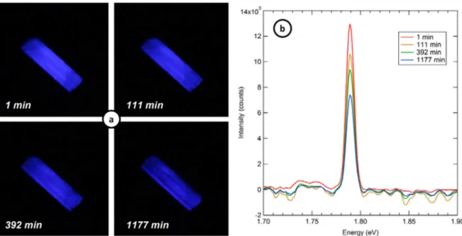
An annealed coated sample was irradiated for several hours under high electron flux in order to study the evolution of defects and their occupation in an-BN/Al2O3 as a function of
the ionizing dose. For the same reasons noted in section 3.3, an incident energy of 5 keV was used to irradiate the sample.
Figure 9(a) shows the temporal evolution of CL intensity under prolonged irradiation, with a noticeable diminution in the red colour of the sample at lower temperatures. The gen-eral intensity, brightness and hue of CL of the an-BN/Al2O3 sample approach those of the BN substrate over irradiation time. However, some regions of the an-BN/Al2O3 sample
becomes brown (dark spots on the picture in figure 9(a) for 1177 min exposure). On occasion, the sample would abruptly increase in intensity after prolonged beam exposure; this and the asymptotic behaviour suggest that the intensity variations were related to sample charging and a concomitant decrease in power deposited in the sample. This is consistent with the temporal evolution of the surface potential of an-BN/Al2O3,
which after 300 min exposed to a 750 nA · cm−2 20 keV
beam at room temperature reached approximately −3700 V [12, 27].
More specifically, the CL intensity of the an-Al2O3‘ruby’
peak decreases ~50% after 1177 min (figure 9(b)). This decrease could be a result of the surface potential build up described above. Alternately, the decrease could result from CL saturation as the occupancy of final ‘ruby’ trap increases with charge accumulation thereby diminishing the CL trans-ition rate [29]. The CL decrease could also result from chem-ical or structural evolution of the Al2O3 surface from defect
Figure 9. Evolution of cathodoluminescence of an-BN/Al2O3 as a function of irradiation time under electron bombardment of 5 keV at 500
nA · cm−2 and at 110 K: (a) evolution of overall intensity captured through SLR CCD camera photographs. (b) Emission CL spectra
modification, contamination or aging [12]. Further details— related to CL—of the effects of electron irradiation on the electrical aging from an-BN/Al2O3 samples are discussed in
[12, 27].
4. Conclusion
A thorough investigation of defects states in samples of boron nitride (BN), alumina coated BN (BN/Al2O3), and annealed
BN with Al2O3 coating (an-BN/Al2O3) was carried out under
electron bombardment through cathodoluminescence (CL) measurements. The natures and densities of defects and their occupation were studied as a function of incident electron energy and flux, sample temperature, and dose. Evidence sug-gests that much of the broad signature emission attributed to BN was produced in the rough near surface regions of the sam-ples and its CL intensity was diminished by surface charging. The Al2O3 coating deposited through physical vapour
deposi-tion does not have substantial CL-active defects, which could impact the surface conductivity of Al2O3 coating. However,
the vacuum thermal annealing treatment performed on BN/Al2O3 has a very significant effect on CL emissions.
Indeed, this thermal treatment generates many sharp features in the CL spectra ascribed to specific types of defects in the sample and especially in the Al2O3 coating. This increase
of the nature and density of Al2O3 defects states, especially
Cr3+ defects, seems to favour electron transitions and charge mobility under electron irradiation. The influence of temper-ature on electron transitions from the conduction band (CB) and shallow trap (ST) states to red trap levels (upper band of DT) is significant. In fact, these states become predominant when the temper ature decreases and charges in the deeper bands remain trapped. Nonetheless, the CL decreases as a function of time under high electron flux. The ionizing dose deposited in the Al2O3 coating gradually degrades this
mat-erial which affects electron transitions.
Acknowledgment
The authors would like to thank A Jensen and A Souvall of Mat erials Physics Group for their technical support. The authors gratefully acknowledge the laboratories and com-panies which contributed to this international collaboration, including the USU Physics Department, ONERA Toulouse, CIRIMAT and THALES.
References
[1] Jensen A E et al 2013 Properties of cathodoluminescence for cryogenic applications of SiO2-based space observatory
optics and coatings Proc. Society of Photo-Optical Instrum.
Engineers Cryogenic Optical Systems and Instruments Conf. vol 8863 pp 88630A1–10
[2] Helmersson U, Lattemann M, Bohlmark J, Ehiasarian A P and Gudmundsson J T 2006 Ionized physical vapor deposition (IPVD): a review of technology and applications Thin Solid
Films513 1–24
[3] Prokofiev B V 2010 Pyrolytical boron nitride as a window material for high power microwave electron devices 8th
Int. of Vacuum Electron Sources Conf. and Nanocarbon (IVESC) (Piscataway, NJ: IEEE) pp 205–6
[4] Treadaway M J, Passenheim B C and Kitterer B D 1975 Luminescence and absorption of electron-irradiated common optical glasses, sapphire, and quartz IEEE Trans.
Nucl. Sci.22 2253–8
[5] Haubner R, Wilhelm M, Weissenbacher R and Lux B 2002 Boron nitrides—properties, synthesis and applications High
Performance Non-Oxide Ceram II (Structure and Bonding vol 102) (Berlin: Springer) pp 1–45
[6] Fowler J F 1959 Radiation-induced conductivity in the solid state, and some applications Phys. Med. Biol. 3 395–410
[7] Dennison J R 2009 Characterization of electrical materials properties related to spacecraft charging Radiation
Capabilities for the Europa Jupiter System Missions Instrument Workshop (Laurel, MD: Johns Hopkins Applied Physics Laboratory)
[8] Jensen A 2014 Modeling the defect density of states of disordered SiO2 through cathodoluminescence Master
Thesis Utah State University, Logan, UT
[9] Dekany J, Johnson R H, Wilson G, Evans A and Dennison J R 2014 Ultrahigh vacuum cryostat system for extended low-temperature space environment testing IEEE Trans.
Plasma Sci.42 266–71
[10] Wilson G, Dennison J R, Jensen A E and Dekany J 2013 Electron energy-dependent charging effects of multilayered dielectric materials IEEE Trans. Plasma Sci. 41 3536–44
[11] Evans A, Dennison J R, Wilson G and Dekany J 2014 Low-temperature cathodoluminescence in disordered SiO2 IEEE
Trans. Plasma Sci.42 272–7
[12] Guerch K 2015 Etude des propriétés physiques et électriques de matériaux céramiques utilisés en application spatiale
PhD Thesis Université Toulouse III, Paul Sabatier [13] Brillson L J 2012 Applications of depth-resolved
cathodoluminescence spectroscopy J. Phys. D: Appl. Phys.
45 183001
[14] Hovington P, Drouin D and Gauvin R 1997 Scanning 19 1–14
[15] Reimer L 1998 Scanning Electron Microscopy: Physics of
Image Formation and Microanalysis 2nd edn (Heidelberg: Springer)
[16] Wilson G and Dennison J R 2012 Approximation of range in materials as a function of incident electron energy IEEE
Trans. Plasma Sci.40 291–7
[17] International Commission on Radiation Units and Measurements 1984 Stopping Powers for Electrons and Positrons ICRU Report 37 (http://physics.nist.gov/ PhysRefData/Star/Text/ESTAR.html)
[18] Bentabet A 2012 Spherical geometric model for absorption electrons/positrons phenomenon: application to the mean penetration depth calculation Vacuum 86 1855–9
[19] Bentabet A 2014 Range and stopping power energy
relationships for 0.5–30 keV electron beams slowing down in solids: analytical model Mod. Phys. Lett. B 28 1450006
[20] Silly M et al 2007 Luminescence properties of hexagonal boron nitride: cathodoluminescence and photoluminescence spectroscopy measurements Phys. Rev. B 75
[21] Kubota Y, Watanabe K, Tsuda O and Taniguchi T 2007 Deep ultraviolet light-emitting hexagonal boron nitride synthesized at atmospheric pressure Science 317 932–4
[22] Powell C J and Jablonski A National Institute of Standards and Technology 2010 NIST Electron Inelastic-Mean-Free-Path Database: Version 1.2 (Gaithersburg, MD: Institute of Standards and Technology) (www.nist.gov/data/nist71.htm) [23] Starley A, Wilson G, Phillipps L and Dennison J R 2016
Predictive formula for electron penetration depth of diverse materials over large energy ranges Proc. 14th Spacecraft
Centre of the European Space Agency ESA/ESTEC)
(Noordwijk, Netherlands, 4–8 April 2016). [24] Berzina B et al 2005 Photoluminescence excitation
spectroscopy in boron nitride nanotubes compared to microcrystalline h-BN and c-BN Phys. Status Solidi c
2 318–21
[25] Zhang W J, Kanda H and Matsumoto S 2002
Cathodoluminescence of cubic boron nitride films deposited by chemical vapor deposition Appl. Phys. Lett. 81 3356–8
[26] Jin M-S and Kim N-O 2010 Photoluminescence of hexagonal boron nitride (h-BN) film J. Electron. Eng. Technol.
5 637–9
[27] Guerch K, Paulmier T, Dennison J R, Dekany J, Lenormand P and Guillemet-Fritsch S 2016 Electrical properties of annealed and coated boron nitride under electron-beam irradiation J. Spacecr. Rockets 53 1100–4
[28] Hoffmann R and Dennison J R 2012 Measurement methods of electron emission over a full range of sample charging
IEEE Trans. Plasma Sci.40 298–304
[29] Jensen A E and Dennison J R 2015 Defects density of states model of cathodoluminescent intensity and spectra of disordered SiO2 IEEE Trans. Plasma
Sci.43 2925–32
[30] Garcia-Guinea J et al 2001 Luminescence of α-Al2O3 and
α-AlOOH natural mixtures Radiat. Meas. 33 653–8
[31] Kristianpoller A R N 1998 Radiation effects in pure and doped Al2O3 crystals Nucl. Instrum. Methods Phys. Res. B 141 343–6
[32] Powell R C, DiBartolo B, Birang B and Naiman C S 1967 Fluorescence studies of energy transfer between single and pair Cr3+ systems in Al
2O3 Phys. Rev. 155 296
[33] Green B A and Passenheim B C 1977 Broad-band
radioluminescence in electron-irradiated ionic compounds
J. Appl. Phys.48 424
[34] Jonnard P, Bonnelle C, Blaise G, Rémond G and Roques-Carmes C 2000 F+ and F centers in α-Al
2O3
by electron-induced x-ray emission spectroscopy and cathodoluminescence J. Appl. Phys. 88 6413–7
[35] Springis M J and Valbis J A 1985 Red luminescence of color centres in sapphire Phys. Status Solidi b 132 K61–5
[36] Powell R C 1967 The interaction of chronium ions in ruby crystals PhD Thesis Arizona State University, Tempe, AZ [37] Ghamnia M, Jardin C and Bouslama M 2003 Luminescent
centres F and F+ in α-alumina detected by
cathodoluminescence technique J. Electron Spectrosc.