Analysis and Modeling of Capacitive Coupling
Along Metal Interconnect Lines
by
Andrew K. Percey
Submitted to the
Department of Electrical Engineering and Computer Science
in partial fulfillment of the requirements for the degrees of
Bachelor of Science in Electrical Science and Engineering
and
Master of Engineering in Electrical Engineering and Computer Science
at the
MASSACHUSETTS INSTITUTE OF TECHNOLOGY
June 1996
@
Andrew K. Percey, MCMXCVI. All rights reserved.
The author hereby grants to MIT permission to reproduce and
distribute publicly paper and electronic copies of this thesis
document in whole or in part, and to grant others the right to do so.
M ASSACH'USETTS NSTi'U L'
OF TECHNOLOGY
JUN
1
1996
Author...
LIBRARIESDepartment of Electrical Engineering andCo mputer Science
Eng.
May 28, 1996
Certified
by ...
...
...
Jacob White
Professor of Electrical Engineering
",sis
Supervisor
A ccepted ',,
....
I
...
.. .
...
...
F. R. Morgenthaler
Analysis and Modeling of Capacitive Coupling Along Metal
Interconnect Lines
by
Andrew K. Percey
Submitted to the Department of Electrical Engineering and Computer Science on May 28, 1996, in partial fulfillment of the
requirements for the degrees of
Bachelor of Science in Electrical Science and Engineering and
Master of Engineering in Electrical Engineering and Computer Science
Abstract
Electrical signals propagating along metal interconnect lines within contemporary microchips experience significant delay and noise due to capacitive coupling effects. Analysis and modeling of these effects was performed at the author's VI-A Internship company. Numerous CAD circuit simulations were performed to acquire a better understanding of these coupling effects. A program was created to assist circuit designers in analyzing these effects for their particular circuit topologies. Two signal buses that were potentially at high-risk for coupling problems were analyzed in detail, and recommendations were made for reducing such problems. Finally, CAD circuit simulation data was compared with experimental data to determine the modeling accuracy of the CAD tools being used with respect to capacitive coupling.
Thesis Supervisor: Jacob White
Acknowledgments
I would like to express my sincere gratitude to David Chin, my supervisor for my final six-month internship assignment at Intel, for providing me with the opportunity to engage in this thesis work within his group and for supplying the guidance and support necessary to make it a successful endeavor.
I owe much of my happiness and success at Intel to George Dallas, Technical Program Manager with Corporate College Recruiting, who spent much time and effort in helping me to find worthwhile and challenging internships within the company for the past three years and who was always been generous with his honest and friendly advice.
Many thanks to Professor Jacob White, my thesis advisor at MIT, who provided encouragement and direction for the thesis and was very open to the ever-changing plans for the focus and scope of my work.
I especially want to recognize my wonderful parents, Kenneth and Ellen Percey, who have made both my academic and non-academic successes possible by always giving me nothing less than wholly unconditional love, support, and understanding for all of my chosen endeavors. I hope I will always make them proud of me.
Finally, I owe deep thanks to my dear sister, Deborah O'Leary, who first got my foot in the door of the high-tech world, which paved the way for my acceptance into the VI-A program with Intel and all of my successes that have since followed.
Contents
1 Introduction
1.1 Motivation for this project . . . . 1.2 Goals for the thesis work . . . . 1.3 Organization of the document . . . .
2 An 2.1 2.2 2.3
Overview of Capacitance
Capacitance physics and modeling ... Capacitive coupling...
Schematic modeling . . . . 2.3.1 Simple RC models . . . . 2.3.2 Idealized capacitive coupling model 2.3.3 r-RC models . . . . 13 . . . 13 .. . 17 . . . 21 . . . 21 . . . 22 . . . 24
3 A Simulation Program for Modeling Cross-Talk Effects 3.1 Simulation circuit model ...
3.2 Program interface screen ... 3.3 Program results screen ...
3.4 Final evaluation ... ...
4 Cross-talk Simulation Data
4.1 Qualitative summary of simulation results . . . . 4.2 Graphs and tables of simulation results . ...
4.2.2 4.2.3 4.2.4
Noise and delay vs. cross-talk models . ... . . Noise and delay vs. interconnect length, width, and spacing . Noise and delay vs. temperature . ... . . .
5 Cross-talk Analysis of Two Microprocessor Buses 5.1 Simulation modeling ...
5.1.1 Precision calculation of cross-coupling capacitance . 5.1.2 Circuit model ...
5.2 Analysis of bus #1 ... 5.3 Analysis of bus #2 ...
6 Correlation of Experimental to Simulation Data 6.1 Approach used for comparisons . ... 6.2 Models and assumptions . ... 6.3 Model comparisons ...
6.3.1 Accuracy with and without cross-talk effects . . . . 6.3.2 Rising/falling transitions . ...
6.3.3 M etal width ...
6.3.4 Overall correlation results . . . .
7 Conclusions A Xtalk.sim files 51 . . . . 52 . . . . . . 52 . . . . 54 . . . . 55 . . . . 57 58 58 59 60 62 63 63 63 64
List of Figures
2-1 A parallel-plate capacitor: a) physical depiction, b) circuit representation 2-2 Current flow "through" a capacitor . . . . 2-3 Electric fields of a single metal plate over a ground plane for two cases:
2-4 2-5 2-6 2-7 2-8 2-9 2-10 2-11 a) h < W,L, and b) h comparable to W,L ... Electric fields of a single metal line over substrate ... Abstract cross-section of a microchip . ...
Electric fields of multiple metal lines over substrate ...
Capacitance modeling of multiple metal lines ... . . A simple RC circuit model ...
An RC model for interconnect . ...
Idealized model for analyzing the physics of capacitive coupling wr-RC model used for estimating interconnect delay ... 2-12 Segment of complete cross-talk model for both noise
.. . 16 . . . 17 . . . 18 . . . 19 . . . 19 .. . 21 . . . 22 . . . 23 . . . 25 . . . 26 and delay Circuit model for Xtalksim program Sample Xtalksim interface screen . . Sample Xtalk.sim output screen . . . Signal delay vs. length ... Signal delay vs. width ... Signal delay vs. spacing ... Signal delay vs. width and spacing Signal noise vs. width and spacing Signal delay vs. temperature... . . . . . 29 . . . . 31 . . . . . 34 . . . . 46 . . . . 47 . . . . 48 . . . . . 49 . . . . . 49 . . . . 50 3-1 3-2 3-3 4-1 4-2 4-3 4-4 4-5 4-6
4-7 Signal noise vs. temperature ... 50
5-1 Cross-section used for precise capacitance analysis . ... 53
5-2 Two layout possibilities for worst-case capacitive coupling ... 53
List of Tables
Sensitivity tests: metal 1 data . . . . Sensitivity tests: metal 2 data . . . . Sensitivity tests: metal 3 data . . . . Sensitivity tests: metal 4 data . . . . Signal noise vs. simulation model . . . . . Signal delay vs. simulation model . . . . . Signal delay vs. level of cross-talk present
5.1 Summary of simulation results: bus #1 .. 5.2 Summary of simulation results: bus #2 ..
Interconnect experimental/simulation correlation - metal 1 Interconnect experimental/simulation correlation - metal 2 Interconnect experimental/simulation correlation - metal 3 4.1 4.2 4.3 4.4 4.5 4.6 4.7 . . . . 42 . . . . 42 . . . . 43 . . . . 43 . . . . 44 . . . . 45 6.1 6.2 6.3 . . . . . 56 . . . . . 57
Chapter 1
Introduction
This Master's thesis represents the bulk of the work that I performed during my final VI-A internship assignment at Intel Corporation in Santa Clara, CA. I completed this work on metal interconnect coupling effects in the group responsible for the design of an enhanced version of the Pentium ProTM Microprocessor. While my work was intentionally focused to be directly usable by this design group, the effects studied and their implications are generally useful and will be even more important for future microchip generations.
Important note about proprietary material:
Given the setting of this work, sensitive proprietary information must, by necessity, be excluded from this thesis document. This censoring manifests itself in several ways:
1) Microprocessor specifications are left out, including architectural descriptions, and functional unit names.
2) For references to values such as clock speeds and process sizes, which are essential to this work, actual numbers have been replaced with variables.
3) Detailed equations for proprietary simulation models are glossed over with only relatively simple, top-level relations being included.
4) Large tables of raw data are excluded in favor of edited summary tables that still fully detail the most important observations and trends.
5) References to material from internal Intel technical memos, reports, and other sources are not included.
I feel that these compromises in no way detract from the understandability or significance of this thesis work.
1.1
Motivation for this project
Capacitive and inductive coupling effects (also termed "cross-talk", since it is the signal dynamics of adjacent lines which cause most of the effects) are always present to some extent in electronic systems. Within high-density, high-performance microchips, these effects become very significant. As device and interconnect sizes decrease and circuit frequencies increase, signal degradation due to electrical coupling becomes more prominent. These trends are prevalent in microchip design, especially leading microprocessor design where circuit density and clock frequencies are continually pushed to their physical limits.
Within microchips it is the long metal interconnect lines which cause the most concern when considering coupling effects. Buses and other sets of parallel interconnect lines in particular must be closely scrutinized as they are composed of many thin, closely spaced wires, running in parallel for considerable distances on the chip. Coupling along these lines not only slows down the circuit, but also introduces noise (voltage fluctuations), which is especially dangerous for sensitive receiving circuits such as pass gates, domino logic, and clocks.
This work focuses on capacitive coupling effects, disregarding the effects of inductance. The decision to exclude inductance effects was made based on previous investigations performed within the microprocessor group which indicated that while capacitive effects were very significant, inductive coupling would have less than a 10% effect on noise and delay given the project's interconnect geometries and target clock frequencies. Since the simulation tools are only accurate to within about 10% overall, the variation due to inductance is safely disregarded, which greatly simplifies the cross-talk simulation models.
1.2
Goals for the thesis work
Specific goals for this thesis work were not set at the beginning of the project. Rather, the work developed as each stage led naturally to further applications and investigations. A general goal was to create a better understanding of not only the ways in which numerous circuit parameters contribute to capacitive coupling but also the significance of these effects and what can be done to minimize their negative impact.
Several smaller and very specific capacitive coupling investigations had been completed within the group before the commencement of this thesis work. Those reports looked mainly at variations in noise and delay when a particular parameter was varied through some specified range. They did not attempt to create a comprehensive understanding of the complex interactions of all of the circuit parameters involved. An important goal of this work is to provide a broader perspective than previously attained on the issue of capacitive coupling.
Another motivating factor for this work was derived from the circuit design practices of the microprocessor group engineers. Many of the integrated circuit engineers used simulation models to account for the performance effects of capacitive coupling but not for the signal integrity effects because including the latter effect greatly increases the complexity of the cross-talk model1. This thesis work uses comprehensive models to consider both performance and signal integrity simultaneously.
Ultimately, the results of this work were to be used to aid circuit designers by providing a more informed understanding of capacitive coupling effects and how to restructure designs to minimize them.
1In this thesis, good "performance" means short signal delays along the interconnect lines, and
1.3
Organization of the document
Chapter 2 develops the mathematical background and circuit models used for capacitive coupling effects.
Chapter 3 describes the Unix script created to help engineers consider coupling effects in their circuit analyses.
Chapter 4 describes the results of numerous circuit simulations performed to investigate cross-talk effects.
Chapter 5 contains an analysis of the capacitive coupling experienced by the two longest buses on the microprocessor chip.
Chapter 6 provides a comparison of capacitive coupling effects as estimated with simulations against the same effects as measured with physical test chip data.
Chapter 7 contains conclusions based upon the results of the work described in the previous chapters.
Chapter 2
An Overview of Capacitance
2.1
Capacitance physics and modeling
Any two objects that are capable of being electrically charged and which are separated by some dielectric material 1 will form a capacitor. Applying a voltage difference between two such objects leads to a buildup of charge on those objects that is proportional to the capacitance between them. This relationship is described mathematically in Equation 2.1, where Q = charge (measured in Coulombs), C = capacitance (Farads), and V = voltage (Volts). Larger capacitances lead to greater accumulation of charge for a given voltage difference. [1, p. 6501
Q = CV [Coulombs] (2.1)
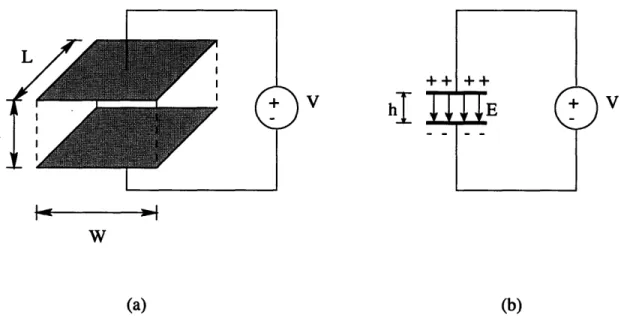
Capacitance can be produced between objects of any shape. The capacitances of concern in this project occur between interconnect lines which, as we shall see, can be fairly accurately modeled as parallel-plate capacitors. For parallel-plate capacitors, the capacitance is given by the relationship in Equation 2.2, where W = the width of the parallel plates (meters), L = the length of the plates (meters), h = the distance
1
A dielectric is any material, including free space, which does not permit current flow, thus
allowing charge to accumulate. Current will flow through dielectrics if the voltage difference is greater than the breakdown voltage of the dielectric. However, for the voltage levels and dielectrics used in this project, dielectric breakdown is not a concern.
between the plates (meters), and E = o-er (Farads/meter) where ~o is the permittivity
of free space (8.854 - 10-6 pF//m) and E, is the relative dielectric constant of the material between the plates. [1, p. 653]
WL
h [Farads] (2.2)
These geometries are shown in Figure 2-1(a). The plates are idealized as having zero thickness. In the remainder of this thesis, references to capacitors will imply parallel-plate capacitors.
hI
w
I
W
(a)
(b)
Figure 2-1: A parallel-plate capacitor: a) physical depiction, b) circuit representation
Placing a voltage across a capacitor produces an electric field, E, between the plates of the capacitor as shown in Figure 2-1(b). The electric field, by definition, is directed from the more positively charged plate towards the more negatively charged plate and is inversely proportional to the distance separating them, as given in
Equation 2.3. [1, p. 653]
V E = h
h [Volts/meter] (2.3)
will "flow" through the capacitor corresponding to Equation 2.4, where ic is the current flowing through the capacitor (Amperes), Vc is the voltage across the capacitor (Volts), and t is time (seconds). [2, p. 126]
ic = C. dV [Amperes] (2.4)
dt dt
As already mentioned, current will not actually flow through a dielectric unless it experiences break down, but the effect here is equivalent. Figure 2-2 demonstrates this graphically.
ic
+
dVC
dt
ic
Figure 2-2: Current flow "through" a capacitor
As the voltage across the capacitor in Figure 2-2 increases (due to voltage changes in the "rest of circuit" black box), electrons (negative, mobile charge carriers) are pushed from the upper plate of the capacitor to elsewhere in the circuit, while electrons are pulled to the lower plate. Electrons exiting the upper plate leave behind a concentration of positive charge on that plate, while electrons accumulating on the bottom plate create a buildup of negative charge there. This effectively creates current flow2 "through" the capacitor from the upper plate to the lower plate. When the voltage level finally stabilizes, the top plate is left with Q (= CV) Coulombs of
2
Current is defined to flow from the more positive voltage to the more negative voltage, which is opposite the flow of electrons.
positive charge, while the bottom plate has
Q
Coulombs of negative charge. [2, p.126-7]
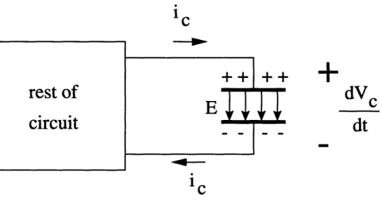
A parallel-plate capacitor can also be created between a single thin plate and a thick plane. Figure 2-3 shows two cases of a single metal plate forming a capacitor with a ground plane. Here, the metal plate is charged to some positive voltage, while the ground plane is at 0 Volts (also termed "V,,"). Imagine that the plates are rectangular with length (the dimension going "into" the page) about equal to the width. Va I Vb
Eb
4(b)
(a)
Figure 2-3: Electric fields of a single metal plate over a) h < W,L, and b) h comparable to W,L
a ground plane for two cases:
In Figure 2-3 (a), the height above the V,, plane, h, is much less than both the width and the length of the metal plate. For this case, the total electric field is dominated by the vertical field and the small "fringing" fields (fields that extend beyond the area of the plate) can be ignored. In Figure 2-3 (b), however, the three dimensions are comparable and the fringing fields are no longer negligible. These fringing fields act to increase the effective area of the plate. Accounting for these
4
I
1P
fringing fields is complex and often ignored when modeling simplicity is important. It should be noted, however, that Equation 2.3 only explicitly holds within regions where E is orthogonal to the parallel plates (i.e., where there is no fringing effect).
[3, p. 191]
2.2
Capacitive coupling
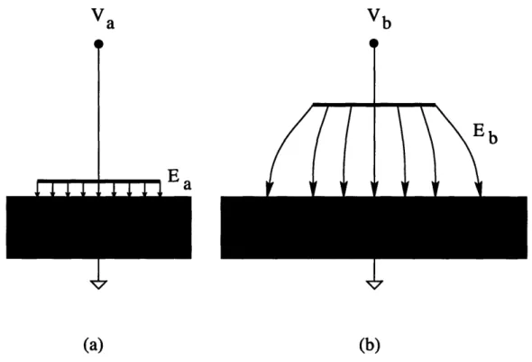
Analyzing real metal lines adds another dimension to this problem because metal lines also have a non-zero thickness, t. A representation of the fields produced by a metal interconnect line is shown in Figure 2-4. The metal line is charged to V,, (logical "1", the highest voltage level intentionally present on the chip), while the substrate below is tied to V,, (logical "0", the lowest voltage level intentionally present on the chip). Note that now the fringing fields are even more prominent than before. Also note that actual interconnect wires may have rectangular cross-sections of any dimensions and are certainly not limited to the square shape shown in the figure. [3, p. 191]
V
Figure 2-4: Electric fields of a single metal line over substrate
Capacitive coupling along interconnect lines refers to the effects experienced by an electrical signal wire due to voltage fluctuations on nearby signal wires. When
dealing with interconnect, these local voltages are produced either by neighboring metal lines (to the side, above, or below) or by the substrate below them. When voltage levels on interconnect lines change, charge flows between the lines due to the capacitive coupling present, as was revealed by Equation 2.4. This flow of charge affects both signal propagation delay (circuit performance) and noise levels (signal integrity). The capacitances present are called "parasitic" capacitances because they are almost always undesired and act to harm performance and signal integrity.
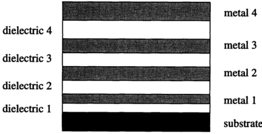
Modern microprocessor designs use multiple layers of metal, each of which has parasitic capacitance to every other layer as well as to the same layer. A cross-section showing the different layers of a microchip is presented in Figure 2-5. Note that the fabrication process used by the design group allows for four distinct metal layers. The metal and dielectric thicknesses are on the order of tenths of microns (millionths of a meter). metal 4 dielectric 4
Smetal
3
dielectric 3metal 2
dielectric 2 metal 1 CU.LI1CLU1L I substrateFigure 2-5: Abstract cross-section of a microchip
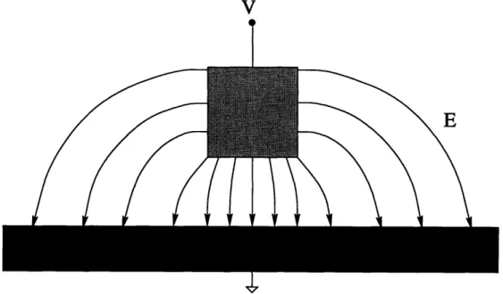
The problem of estimating capacitance for calculating its effects becomes even more complicated when multiple metal lines are considered. Figure 2-6 shows a complete picture of the electric fields present in a 3-metal parallel configuration.
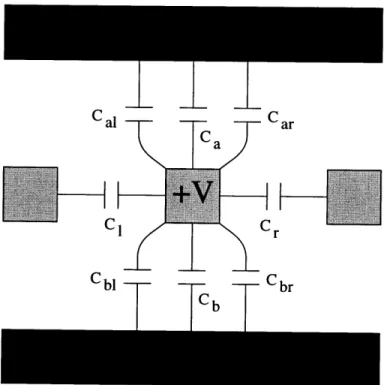
When running waveform simulations on large circuits it becomes prohibitive to attempt to analyze every electric field present to get a completely accurate view of the capacitances and their effects. The "compromise" model used by the simulation tools in this project is shown in Figure 2-7. The upper and lower rectangles simulate
AA/
61`11i
I
Figure 2-6: Electric fields of multiple metal lines over substrate
C
al C ar Cl C-C1 r Cbl C br Cb"'iTc
T
Figure 2-7: Capacitance modeling of multiple metal lines
%,
\Xl f / l ·S
AA/ • f Jfull metal coverage. The top rectangle can be removed, indicating that there is no metal coverage above the signal line. There may also be no metal coverage below the signal line, in which case the lower rectangle represents the substrate.
The equation used to calculate the overall capacitance seen by the central metal line of Figure 2-7 is given in Equation 2.5 with the term definitions following. This model has been experimentally proven in previous investigations using an electromagnetic field solver program to yield values for total capacitance that are accurate to within 10% of the actual values.
Ctotal = Ca + Cb + Ca, + Car + Cb, + Cb + K
-
C, + K . Cr (2.5)Ca = area capacitance to the layer above Cb = area capacitance to the layer below Cat = fringing capacitance to the above left Car = fringing capacitance to the above right Cbl = fringing capacitance to the below left Cbr = fringing capacitance to the below right
C, = line-line capacitance to the left Cr = line-line capacitance to the right K = Miller capacitance factor (constant)
The constant, K, is used to try to compensate for adjacent lines in the same metal layer which may be experiencing voltage changes different from the line of interest in the center. This is very often the case in buses. K can be assigned by the circuit designer the values 0, 1, or 2, depending on the application, and it will be explained in detail later.
2.3
Schematic modeling
2.3.1
Simple RC models
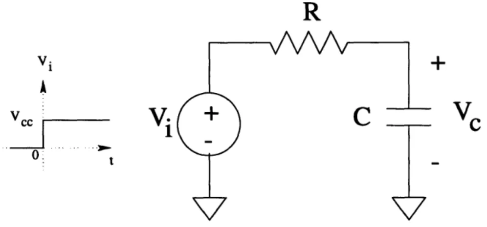
Delay along long interconnect wires is "RC dominated", meaning it is the combination of the resistances and capacitances along the line which has the most significant influence on delay. For a simple RC circuit, as shown in Figure 2-8, the output is given by Equations 2.6 and 2.7 for an ideal voltage step input. It is apparent from these equations that a larger RC product corresponds to slower voltage swings across the capacitor. [2, p. 139-47]
R
V i AVcc.
V
0 t+
Figure 2-8: A simple RC circuit model
(charging) Vc = V, - (1 - e- t/Rc) [Volts] (2.6)
(discharging) Vc = Vec -e- t/Re [Volts] (2.7)
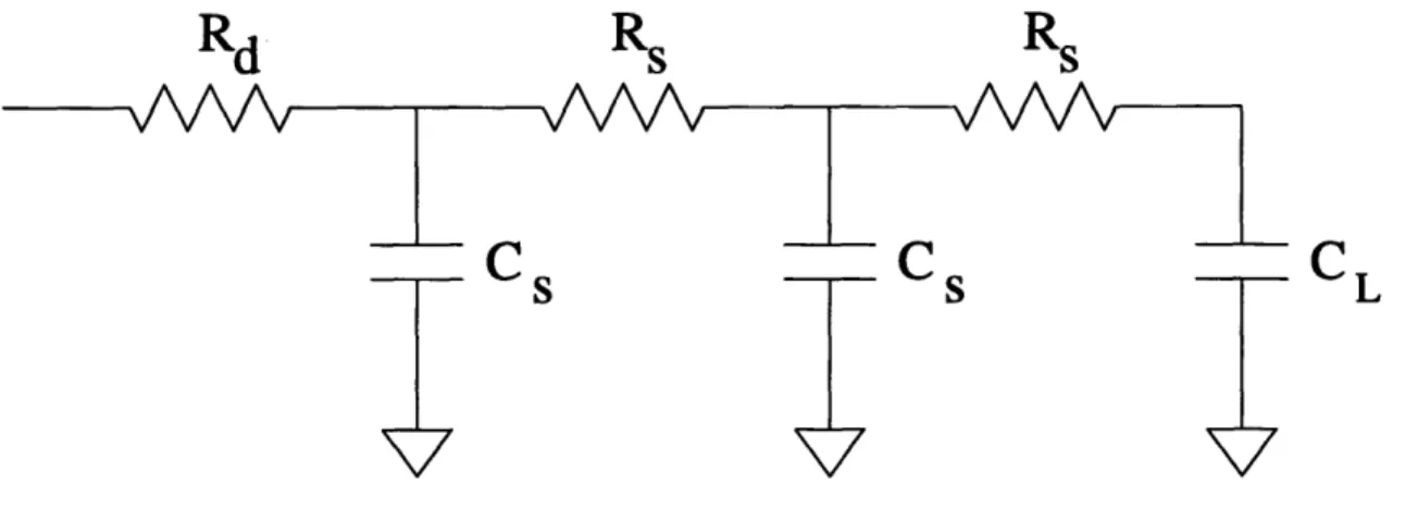
Fully modeled interconnect lines add much complexity to this model. A model for interconnect is shown in Figure 2-9, where C, is the capacitance of each segment, C, is the capacitance of the receiving element (also called the "load"), R, is the resistance of each segment, and Rd is the resistance of the driving element.
Rd
R
sR
sSs
sL
Figure 2-9: An RC model for interconnect
circuit is given in Equation 2.8. Any number of R,/C, segments could be used in this model. The more segments used, the more the model will approach a "true" description of the wire, which can best be thought of as being made up of an infinite number of infinitesimally small RC segments. [3, p. 198-200]
m n
(RC)total - -[Ci -E(Rj)] = (Rd) -Cs + (Rd + Rs) -Cs + (Rd + 2Rs) -C1 (2.8) i=1 j=1
For interconnect lines, R is calculated from Equation 2.9, where p is the resistivity of the metal (Ohm - meters) [1, p. 678-81], and C is calculated from Equation 2.2.
L
R= p -. [Ohms] (2.9)
2.3.2
Idealized capacitive coupling model
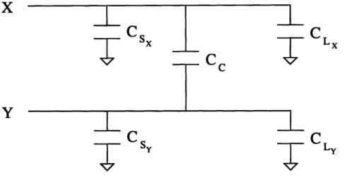
To understand capacitive coupling, it is instructional to consider the idealized case presented in Figure 2-10, which shows two coupled lines with all resistances removed from the model. Cs is the self-capacitance of each interconnect line, CL is the capacitance of each receiving load device, and Cc is the cross-coupling capacitance present between the two parallel lines.
I I I
T
SxLx
Y
Tcy
TcLy
Figure 2-10: Idealized model for analyzing the physics of capacitive coupling
(to V,c). If X now switches low (to V,,), then it has to discharge the charge stored on capacitors, Csx, CLx, and Cc. Capacitance adds when capacitors are in parallel, so the Ct,oat that needs to be considered in the instantaneous transient for signal line X is Csx + CLx + Cc. If the coupling to line Y was not present, then there would not be a Cc capacitor and hence no Cc term in Ctot. Therefore, with capacitive coupling there is more stored charge to remove in order to switch the line low, which results in slower signal propagation and transition times.
To understand how voltage glitching occurs, consider what happens to Y in the previous example. When X and Y are both high, there is no voltage drop across Cc. Assuming that Y is not being actively driven (i.e., it is a "floating" node), then the voltage on Y is maintained by the charge on Csy and CLy. Thus, the initial voltage on Y is:
QY
Vy = ( y+ (2.10)
(CsY + CLY)
But when X switches low, Cc is suddenly thrown into the picture. When the transient on X has passed, Y now "sees" three capacitors to ground, but the total charge stored on Y has not changed because it is an isolated node. So now, the final voltage on Y is:
QY
VY = +L ) (2.11)
(CsY + CLy + CC)
Combining Equations 2.10 and 2.11 yields Equation 2.12, which clearly shows the final voltage on Y to be less than the initial voltage when there is capacitive coupling present.
S
(
+
CL)
(2.12)
YV (Cs + CLY + c) (2.12)
This analysis is idealized but easily expanded to include realistic situations. If Y were a long, driven, resistive line, then the portion of the line at the load end can be considered to be a temporarily floating node. When X switches, Vy will drop as noted above, but will recover through the influence of its driver. The voltage dip and recovery will both be exponential with RC rather than instantaneous as in the idealized case. This dip is dangerous even when temporary because it may cause the receiving element to change its logical output, a logical error which could in turn propagate through the rest of the circuit.
2.3.3
7r-RC
models
The values used to calculate the individual terms of Ctot, in Equation 2.5 are acquired from two places: from the process file for the fabrication process being used, and from the designer, who provides the length, width, and spacing of the lines, the metal layer and coverage by other layers, and a value for K. This information, as well as resistance information that is also read from the process file, is incorporated into circuit schematics by using the 7r-RC model shown in Figure 2-11. This r-RC model is instantiated in schematics to model delay due to resistance of the line and due to the self- and cross- capacitances present.
The r-RC model is often instantiated several times along a single schematic wire in order to yield a more accurate, distributed RC model rather than a simple, lumped (single R, single C) RC model. The 7r-RC model can only be specified within the simulation tool to have either zero or complete overlap with any metals above it
Figure 2-11: 7r-RC model used for estimating interconnect delay
or below it or with the substrate. This "all or nothing" modeling shows the value of using multiple ir-RC models along the same line so that overlap variations can be approximated with different specifications for each 7r-RC model. All of this information is then used to select the appropriate parameter values from the process file for the resistance and capacitance calculations.
One significant limitation of this 7r-RC model is that it has no facility for incorporating noise effects due to capacitive coupling to adjacent lines. This shortcoming is present because each interconnect line has no information about the dynamic voltage levels on adjacent lines. To incorporate this important information, explicit cross-coupling capacitors must be included in the schematic. A complete section of 3 adjacent, same metal layer interconnect lines with distributed 7r-RC modeling and explicit cross-capacitors is shown in Figure 2-12.
Simulation results for circuits using ir-RC modeling vary considerably depending on the value chosen for K, which is used in Equation 2.5. To understand the role of K, refer to Figure 2-12, but ignore the cross-capacitors for now and consider delay only. Setting K = 0 is the best case for delay. It assumes that both adjacent lines are switching along with the center line, either all from low to high or all from high to low, so that dV/dt = 0 (in Equation 2.4) and the capacitances between them, therefore, have no effect. Since dV/dt cannot be set to zero within the model, K is set to zero, which eliminates the capacitance contribution from the adjacent lines, thus achieving the same goal. Setting K = 1 means that the voltages on both adjacent lines are remaining constant while the center line switches, so that capacitance to these lines
Figure 2-12: Segment of complete cross-talk model for both noise and delay
is felt. Finally, setting K = 2 is the worst case for delay. It means that both adjacent lines are switching in the opposite direction of the center line so that the dV/dt is essentially doubled. Since in this case there are no explicit cross-capacitors to model dV/dt in the simulation, the K value is needed to appropriately scale C, and Cr in Equation 2.5. Note that only delay can be modeled by varying K, not noise.
Now consider the full model of Figure 2-12. Not only do the explicit cross-capacitors allow switching on the adjacent lines to cause voltage glitching (noise) on the center line, but dV/dt is explicit in the simulation so that K values are not needed. Indeed, for this complete simulation schematic, the K values of all the 7r-RC models are set to zero, else the capacitance effects would be counted twice! By setting K = 0, we are removing all line-line coupling estimation from the 7r-RC model, instead accounting for such coupling explicitly.
The values for the cross-coupling capacitors must also be retrieved from the process file, based upon metal layer, spacing, and segment length. It was the additional complexity introduced through using explicit cross-coupling capacitors that led many
V
-T
V
T
v v
designers to forsake this full coupling model for the simplicity of the simple wr-RC model. Note that this full model is not only more satisfying in its completeness in providing a way to measure noise, but it is also more accurate in its delay calculation in most cases, as will be shown in Chapter 6.
It is important to understand why all of this circuit estimation is performed when much more accurate circuit values can be extracted from layout and more accurate cross-coupling analysis performed at a later stage of the project. The benefits are gained because improving the circuit level timing and noise analysis has been shown to greatly reduce the amount of debugging required after the layout phase. Furthermore, as circuit designers become accustomed to accurately modeling parasitics, they will naturally learn to optimize their circuits for such effects from the outset, again minimizing debugging time.
Chapter 3
A Simulation Program for
Modeling Cross-Talk Effects
My initial approach for improving engineers' understanding of cross-talk effects within the project group was to create a series of graphs that plotted variations in signal delay and noise due to each contributing parameter. It soon became apparent, however, that this approach would have limited usefulness because of the number of parameters involved and their intricate interactions. Faced with this problem, I thought of and developed the idea of creating a program, called "Xtalk.sim", which could account for all relevant parameters simultaneously.
The goal of this program was to provide a straightforward means for engineers to analyze capacitive coupling in their circuits without needing to create elaborate models themselves. The simulation program was written using the C-Shell programming language. This language was chosen for its straightforward means of interfacing with the circuit simulation tool. The C-shell script creates an interactive interface through which engineers may specify numerous parameters relevant to their interconnect lines of interest. After the relevant data has been entered, a simulation is spawned using a circuit model whose values are governed by those input parameters. When the simulation completes, the results are displayed in an Emacs window. The hope was that this program would become a useful addition to the current design flow in the microprocessor group.
3.1
Simulation circuit model
The full circuit model, complete with variable parameters, is shown in Figure 3-1. This cross-talk model is an embellished version of the circuit of Figure 2-12. The inputs, Xi, Yj, and Zi are fed into inverting drivers, which drive the signals down the long interconnect lines into inverting receivers, to produce the outputs, Xo, Yo, and
Zo.
Xo
Yo
Zo
T "L
Figure 3-1: Circuit model for Xtalk-sim program
Note that every circuit element in the simulation model has a variable assignment which is determined from the user inputs. The drivers, receivers, metal layer, metal coverage, metal length, metal spacing, metal width, cross-coupling capacitances, optional additional load capacitances, and even input signal rise and fall times are all variable. Some of these parameters are assigned directly from the user inputs,
while others are either calculated or looked up in the process file for the project. The Xtalk-sim program handles all of these variable assignments. Note that each of the three adjacent signal paths are identical with the exception that the outer paths are not coupled to further metal lines.
3.2
Program interface screen
A sample of the interface created when Xtalksim is run is shown in Figure 3-2. Every choice for which the user is prompted has a default value (listed in <>, and given here as a variable name) which can be kept by simply pressing return (< CR >). The program requests information about the drivers, the receivers, the input waveforms, and the interconnect, and it also includes a few extra options.
For both the driver and receivers, specific inverter-like library cells can be specified, as these are the most common driver and receiver elements for long interconnect lines. A non-inverter-like gate can be approximated by specifying the effective p and n transistor sizes of the gate, which are then used to calculate output drive and input capacitance. Adding the capability to directly specify any type of gate from the libraries available would have greatly complicated the program while adding little utility, so was not included. For the receiver specification there is a third option: specifying a capacitive load (in which case the receiving gates are removed from the circuit). This is useful for cases either where there are multiple receiving elements or else where the receiver is not an inverter and the input capacitance of the gate is more readily available or more accurate than a value calculated from the effective p
and n sizes.
The sample shown assumes that the default choice of specifying explicit library cells was selected. In this case, the further options of choosing inverter libraries and exact drivers are presented. If the choice of indicating effective p and n transistor sizes had been made, then the program would have prompted for those values. Finally, if the capacitive load option had been selected, a capacitive value in units of picofarads would have been requested.
##########################
# XTALK_SIM version 2.0 # # Created on 10/13/95 by Andrew Percey #
##########################
Enter the following parameters for the interconnect lines (or hit < CR > for default values):
Do you want to specify the driver with:
(1) an explicit library cell
(2) effective p and n sizes for an inverter model choice = < 1 >:
driver library [basic, complex, etc] < basic >: driver type < inv7 >:
Do you want to specify the receiver with: (1) an explicit library cell
(2) effective p and n sizes for an inverter model (3) a capacitive load
choice = < 1 >:
receiver library [basic, complex, etc] < basic >: receiver type < inv7 >:
20%-80% rise time for input to drivers < trie,, NS >: 80%-20% fall time for input to drivers < tfaLL NS >: process corner < prOCdef >:
7r-RC modeling:
total line length < len >:
7r-RC model name < default: metal 2 over substrate >: 7r-RC spacing < sm2 >:
ir-RC width < wm2 >:
fraction of line using this 7r-RC model < 1.0 >: Run extra simulations without explicit cross-capacitors
to compare delays? (y/n) < n >: y
What K value should be used for modeling the delay? K (0,1,2) < 0 >: 2
Run xtalk.sim again? (y/n) n
After the drivers and receivers have been characterized, the program requests information about the input waveforms. Specifically, it will prompt for the rise and fall times of the input signals, where rise and fall times are measured from the 20% to 80% of Vc, points. With this information Xtalksim generates closely-approximated waveforms to be used as the inputs. For example, if the input rise time is tr, then then the generated rising transition will consist of three linear voltage ramps each of duration tr: one from V,, to 20% of V,,, one from 20% of Vc, to 80% of Vc, and one from 80% of Vc, up to V,,.
Next is a request for the "process corner" to be modeled. This parameter defines assumptions about the quality of silicon produced - whether is has faster or slower devices than expected, etc. This specification was included for completeness, but at the time this work was done, the simulation tool did not differentiate between different process corners.
Several parameters are needed to fully characterize the interconnect: the total length of each of the interconnect lines, the metal/substrate coverage model to use, the spacing between each pair of lines, the width of each line, and the percentage of each interconnect line that should use the parameters just entered. The coverage model indicates the metal layer for the current line and also the interactions with other metals above and below or the substrate below. For example, the default model, metal 2 over substrate, indicates no significant overlap with other metals; its only source of coupling capacitance comes from the substrate below. If the "fraction of line" option is kept at 1.0, then all of the ir-RC models in the simulation schematic will be assigned the parameters that were just selected. Optionally, a fraction in multiples of 0.1 (since there are 10 wr-RC models along each interconnect line) can be specified. In that case, the r-RC modeling input section will repeat, allowing different characterization for further sections of the interconnect until 100% characterization is achieved.
Next, a further option is presented. If desired, a second set of simulations can be run. In this optional set of runs, the explicit cross-coupling capacitors are effectively removed from the circuit and instead K values are specified. This option was made
available so that designers who were accustomed to the simple K value modeling could easily see how much of a difference the full characterization makes in delay analysis. After this option, the circuit database is built and the simulations are spawned.
Finally, the user may choose to re-run Xtalksim. This can be done immediately because the simulations running are spawned as background processes in Unix. If the program is re-run, all of the values that the user just specified become the default values.
The simulations performed are for worst case scenarios. For noise simulations, the victim line is first held high while the attacking lines switch from high to low then from low to high in unison. Then the victim line is held low and the attacking line pattern is repeated. For delay simulations, the victim line first switches high to low while the attacking lines simultaneously both switch opposite the victim line. Then the victim line switches low to high while the attackers again switch oppositely.
3.3
Program results screen
Figure 3-3 shows a sample Xtalksim output screen that resulted from running simulations with the parameters that were chosen from within the interface screen of Figure 3-2. This output screen has two main sections. The first half restates the input values that were specified by the designer. The second half gives the noise and delay values calculated by the circuit simulator.
The simulation results section is further broken down into two sets of data. In the first, the attacking lines (the two lines surrounding the "victim" line of interest) are switching from low to high (rising), while in the second, the attacking lines are switching from high to low (falling). A glance at the numbers will reveal that both noise and delay are considerably worse in the second set of data. This trend is explained by the fact that in the default driver as well as in most of the drivers in the cell libraries used, the pull-down devices (NMOS transistors) are stronger than the pull-up devices (PMOS transistors).1
XTALK-SIM SIMULATION RESULTS
Simulation parameters chosen:
driver library: basic
driver type: inv7
receiver library: basic
receiver type: inv7
driver input rise time: trise
driver input fall time: tfall process corner: prOCdef
total line length: len
ir-RC model: metal 2 over substrate spacing: sm2 width: w,n2 fraction of line: 1.0
Simulation results - worst case effects on victim line:
%%%%%%%%%%%%%%%%%%%%%%%%%%%%%%%%%%%%%%%%%%%%%%
% Attacking lines RISING from V,, to V,,: %
% Voltage glitch from V,,: +.1726 V %
% Voltage glitch from Vcc: +.3291 V %
% Delay with cross-caps K = 2 %
% Interconnect delay: .0202 NS .0256 NS %
% Driver delay: .1268 NS .1603 NS %
% Total delay: .1470 NS .1859 NS %
%%%%%%%%%%%%%%%%%%%%%%%%%%%%%%%%%%%%%%%%%%%%%%%%%
%%%%%%%%%%%%%%%%%%%%%%%%%%%%%%%%%%%%%%%%%%%%%%%
% Attacking lines FALLING from Vc, to V,,: %
% Voltage glitch from V,,: -.2692 V %
% Voltage glitch from Vcc: -.5176 V %
% Duration IV9litchl > 20%Vcc: .1078 NS %
% Delay with cross-caps K = 2 %
% Interconnect delay: .0206 NS .0301 NS %
% Driver delay: .3515 NS .3107 NS %
% Total delay: .3721 NS .3408 NS %
%%%%%%%%%%%%%%%%%%%%%%%%%%%%%%%%%%%%%%%%%%%%%%% average (cross cap)/(total cap) along victim line = 0.930
Therefore, the attacking lines switch more quickly during the falling transitions, leading to a greater "current" flow through the cross-coupling capacitors in the model, increasing both noise and delay along the victim line.
Both sets of data give the same information. Consider the set with the attacking lines rising. The first piece of data is the level of the voltage glitch when the victim line is being driven low. The voltage glitch is measured at the input to the receiver, where noise is of most concern. In this case, the victim line rises to about 0.17V temporarily, due to the low to high transitions of the attacking lines, before being driven back down to OV by its driver.
The second data is the level of the voltage glitch when the victim line is being driven high. In this case, the victim line actually rises above Vc, by about 0.33V before settling back down to Vc. The trend within the noise data is that the glitch is always worse when the victim line is being driven high than when it is being driven low. Again, this effect is a result of the driving pull-up device being weaker than the pull-down device and therefore less able to maintain a steady voltage level in the presence of capacitive coupling.
Note that the second set of results data has an additional line following the "Voltage glitch from Vc" value. If any of the output voltage glitches exceeds 20% of Ve, in magnitude, then an additional line of data is reported which reveals the duration of time for which that threshold is exceeded. This information is provided to help the user visualize the noise to distinguish between a very brief noise spike and a longer-lasting glitch. The latter is more dangerous in terms of causing the receiving stage to switch, which could lead to a logic error.
Finally, delay information is reported, split into the sub-categories of interconnect delay (delay from the output of the driver to the input of the receiver), driver delay (delay from the input of the driver to the output of the driver), and total delay (the sum of interconnect and driver delay). As throughout this thesis, delay is measured
and P type MOSFET transistors, which can only be overcome by making the P devices larger than the N devices, which is often done. By default, however, drivers with same size N and P transistors can drive the output low more strongly (i.e., more quickly) than they can drive the output high.
at the 50% of V,, points.
At least one, and optionally two, columns of data are given for delay information. The first column presents the results of the simulations run with the full cross-coupling capacitor circuit model and K = 0. The second, optional column gives delays from simulations in which the cross-coupling capacitors are removed and instead the K value is used to approximate coupling effects. As explained previously, this option was included for engineers who were accustomed to such modeling.
Note that for the parameters given for this simulation run, the driver delay is much more significant than the interconnect delay. For longer interconnect lines, the interconnect delay component becomes a much more substantial and, eventually, dominant part of the full signal delay.
At the bottom of the output screen is a report of the average cross-coupling along the victim line in terms of a (cross - couplingcapacitance)/(totalcapacitance) ratio. This number was included also as a reference for engineers accustomed to using this ratio to determine potentially problematical interconnect lines. This ratio by itself, however, does not encompass all of the relevant parameters. For example, changing any of the length, driver, receiver, or input waveform parameters will alter both noise and delay along a capacitively coupled line, but will not change the % cross-cap ratio. Too much importance, therefore, must not be placed on this ratio without full knowledge of all of the circuit parameters.
3.4
Final evaluation
Xtalksim was designed to have many features desirable for circuit designers who are concerned with capacitive coupling in their circuits. The program offers a much quicker alternative for accurate coupling analysis than creating a full 7F-RC and cross-capacitance model for each metal line in a circuit schematic. The interface is straightforward and simple to use. Any number of simulations can be spawned simultaneously, with values from one simulation conveniently appearing as the default values for the next so that testing of limited parameter tweaking is very simple.
Finally, the set of simulations run by each execution of Xtalk.sim requires only about
1 1/2 minutes of CPU time to complete, so results are very quickly attainable.
Xtalksim, as written, performed all simulations at To Celsius. As both noise and delay exhibit slight changes in performance due to temperature (as described in Chapter 4), including temperature as a specifiable variable in the interface screen would be a worthwhile future addition.
Chapter 4
Cross-talk Simulation Data
During the course of the work I performed at Intel, I ran a large number of circuit simulations to investigate cross-talk effects. The results of some of the more revealing ones, which provide insight into the effects of capacitive coupling, are included in this chapter.
4.1
Qualitative summary of simulation results
Performance problems (delay) and signal integrity problems (noise) are affected to different degrees and, in certain cases, in different ways by the same circuit parameters. These parallels and differences are discussed below and exemplified in the tables and graphs of this chapter.
Signal propagation delay is governed by the time required to charge or discharge capacitances, parasitic and otherwise, along the interconnect line. In general, the capacitance of the receiving element is the most critical, but as line lengths and, therefore, cross-coupling, increase, interconnect capacitance becomes more and more important.
Signal noise is introduced by dynamic voltage switching on adjacent interconnect lines. As line lengths increase, the metal lines behave more like floating nodes because the driving elements are relatively far away so that it takes significant time to recover from voltage fluctuations. This effect makes long metal lines more susceptible to
cross-talk noise, especially at points close to the receiving elements (the farthest from the driver a line segment can be), which, unfortunately, is where voltage stability is the most important.
The circuit conditions leading to noise are a slightly different set than those leading to delay, but they both have many factors in common. Decreasing spacing between metal lines increases the cross-capacitance between the lines, adversely affecting both noise and delay. Decreasing the metal width of the wire increases noise susceptibility because the self-capacitance is reduced so that the cross-capacitances play a more significant role, while smaller width also means larger resistance through the metal so that delay is increased. Also, a smaller driver for the victim line (buffer, inverter or whatever it may be) means the signal is driven more weakly so is more susceptible to noise effects and also takes longer to (dis)charge line capacitances, thus increasing delay. Finally, as circuit temperatures increase, wire resistances increase, which directly increases delay (through the RC product) and indirectly increases noise by further isolating the receiver from its driver.
There are also several parameters that affect noise and delay oppositely. A large capacitive load at the end of the line due to the receivers helps maintain voltage levels and hence reduces noise effects, but it also increases (dis)charge time. Fast input transitions (short rise and fall times) cause more noise because of the increased dV/dt, but can actually help delay when measured as we are measuring it, using 50% of Vcc points, because the line and load capacitances are (dis)charging while the input has yet to swing to 50%, thus giving the output signal a "head start". Having non-switching metal or substrate above and/or below the line helps reduce noise by adding "quiet" capacitance, but it increases delay because of this same additional capacitance.
4.2
Graphs and tables of simulation results
A number of tables and graphs of data were produced that explicitly show these noise and delay effects due to capacitive cross-coupling. Most of the data was generated
using Xtalksim and the full ir-RC model shown in Figure 3-1, which includes explicit cross-coupling capacitors with the K coefficient set to zero. Any deviations are noted within the relevant sections. The simulations that were run to produce all of these tables and graphs use the parameter values below as defaults except for the particular parameter that is being varied.
default 7r-RC model = metal x over substrate with no overlap of other metal layers default spacing = sm, = minimum spacing of metal x
default width = wm, = minimum width of metal x default length = len
default driver size = buf7
default receiver size = buf7
default rise time = trise default fall time = t all
default temp = To
These default parameters were chosen based upon average or customary parameters for circuits in which cross-talk concerns arise. The default ir-RC model of "metal x over substrate with no overlap of other metal layers" makes the cross-coupling to the adjacent metal lines dominant, leading to worst case noise glitching. Spacing and width are set to minimum for worst case noise and delay modeling. The length was made sufficient to produce substantial variations in noise and delay when other parameters were varied. The driver and receiver were set to the typical bus driver/receiver inverter. The rise and fall times were set to typical times for the target clock speed. The default temp was set to the minimum test value.
Initially, a model with 20 7r-RC elements modeling each interconnect line was used for performing simulations. Changing the model to use only 10 7r-RC elements, however, led to less than a 1% difference in noise and delay calculations while decreasing computation time by more than 20%. Thus, the 10 element model was chosen for performing simulations.
4.2.1
Broad-range sensitivity tests
The following "sensitivity" experiments were performed to get a "feel" for the effects of individually varying all the parameters that change the influence of capacitive coupling. A summary of the changes in noise and delay for metals 1 through 4 are presented in Tables 4.1 through 4.4, respectively.
The first column of each of these tables lists the parameter that is being varied from its default value. For example, the second data row reads: "spacing: 1.5. smX", which indicates that the data in that row was produced by simulations run using the default parameters except for spacing, which was increased by 50%. Also, "buf8" is
one inverter size larger than "buf7", and so on. For simplicity and symmetry, the
tests were run with tris = tfall = ttran,,. Reading the data, in Table 4.1 increasing the spacing by 50% decreases the worst case voltage glitch by 23% and worst case total delay by 10%. The percentage changes listed in the sensitivity tables are the worst case changes found from examining the results of all input transition combinations. Total delay is the sum of line (interconnect) delay and driver delay; For these examples driver delay makes up a more significant portion of the total delay. The final column gives the change in the cross-cap ratio, which was introduced in Chapter 3.
Studying these tables reveals many prominent trends which hold in general across all of the metal layers. In fact, taking metal 3 as a base line data set, all of the other metals exhibit the exact same behavior for all of the given parameter changes to within 5% (except for metal coverage values which vary up to 10%). Notice that changing the 7r-RC model from one with no metal coverage above or below the current metal layer to one with full coverage has the greatest impact on reducing the level of the voltage glitching experienced. Increasing the spacing also significantly reduces noise. Increasing the length of the interconnect greatly increases noise, of course. And making the rise/fall transitions sharper also worsens noise. In terms of delay, length is the most influential dimension, obviously. A stronger driver will significantly improve signal propagation time, as will faster input transitions and wider spacing. All of these trends are exactly as discussed in Section 4.1, which details the reasoning
Table 4.1: Sensitivity tests: metal 1 data
(cross cap)/
voltage glitch total delay line delay driver delay (total cap) parameter changed % change % change % change % change % change
ir-RC model: full coverage -32 -1 +7 -2 -33
spacing: 1.5-Sm, -23 -10 -8 -10 -13
width: 1.5-Wm, -5 -1 -34 +3 -3
length: 1.5-len +31 +28 +89 +20
-driver: bufs -6 -14 -3 -15
receiver: buf8 -7 +4 +14 +2
rise/fall time: 0.5"ttran +14 -16 +3 -18
Table 4.2: Sensitivity tests: metal 2 data
(cross cap)/
voltage glitch total delay line delay driver delay (total cap) parameter changed % change % change % change % change % change
7r-RC model: full coverage -47 -4 +10 -5 -48
spacing: 1.5-Sm2 -21 -10 -9 -10 -9
width: 1.5Wim2 -4 -1 -34 +2 -2
length: 1.5-len +32 +26 +85 +22
-driver: buf8 -8 -14 -3 -15
receiver: bufs -6 +4 +17 +3
-rise/fall time: 0.5-ttran +16 -16 +1 -17
Table 4.3: Sensitivity tests: metal 3 data
(cross cap)/ voltage glitch total delay line delay driver delay (total cap) parameter changed % change % change % change % change % change
7r-RC model: full coverage -42 -6 +3 -7 -40
spacing: 1.5-sm, -20 -9 -8 -9 -9
width: 1.5-wm, -3 -1 -35 +1 -1
length: 1.5-len +32 +26 +87 +22
-driver: bufs -7 -14 -3 -15
receiver: bufs -6 +4 +17 +3
Table 4.4: Sensitivity tests: metal 4 data
(cross cap)/ voltage glitch total delay line delay driver delay (total cap)
parameter changed % change % change % change % change % change
7r-RC model: full coverage -34 +2 +12 +2 -39
spacing: 1.5-s,4 -28 -11 -6 -11 -15
width: 1.5-wm, -2 +1 -31 +1 -2
length: 1.5-len +31 +23 +84 +23
-driver: buf8 -11 -15 -6 -15
-receiver: bufs -6 +4 +19 +4
-rise/fall time: 0.5-ttran +18 -17 +0 -17
-behind these results.
4.2.2
Noise and delay vs. cross-talk models
Tables 4.5 and 4.6 show the results of simulations run with various circuit configurations. Table 4.7 shows the results of simulations run with various cross-talk models. All of these tables use metal 2 for the simulation models.
Table 4.5: Signal noise vs. simulation model glitch with
attacking lines rising attacking lines falling model used from V,, from Vc from V, , from V,,
default
+0.173
+0.329
-0.269
-0.518
1st half: no coverage
+0.120
+0.237
-0.194
-0.377
2nd half: full coverage
full metal coverage +0.087 +0.169 -0.146 -0.272
four attacking lines +0.182 +0.338 -0.272 -0.516
only one attacking line +0.088 +0.179 -0.140 -0.285
two attacking lines +0.081 +0.160 -0.127 -0.249
separated as if shielded
two attacking, shielded lines +0.013 0.022 -0.019 -0.033
Tables 4.5 and 4.6 show two sets of results for the same set of ir-RC models (in the first column). The default model is metal 2 over substrate with no overlap of other metals and with two adjacent, parallel lines set at minimum spacing. The second row