Applications of Emerging Optoelectronic
Materials: Lead Sulphide Quantum Dots and
Steam Cracker Tar
by
Owen P. Morris
M.Sci., University of Glasgow (2014)
Submitted to the Department of Materials Science and Engineering
in partial fulfillment of the requirements for the degree of
Doctor of Philosophy in Materials Science and Engineering
at the
MASSACHUSETTS INSTITUTE OF TECHNOLOGY
June 2019
@
Massachusetts Institute of Technology 2019. All rights reserved.
Signature redacted
A uthor
...
...
Department of Materials Science and Engineering
May 24, 2019
Certified by
Signature redacted
y W/
Jeffrey C. Grossman
Professor of Materials Science and Engineering
Thesis Supervisor
Signature redacted
Accepted by.
MASSACHUSETS INSTITUTE OF TECHNOLOGYJUN 142019
LIBRARIES
Jr /7VDonafd R. Sadoway
Chair, Departmental Committee on Graduate Studies
Applications of Emerging Optoelectronic Materials: Lead
Sulphide Quantum Dots and Steam Cracker Tar
by
Owen P. Morris
Submitted to the Department of Materials Science and Engineering on May 24, 2019, in partial fulfillment of the
requirements for the degree of
Doctor of Philosophy in Materials Science and Engineering
Abstract
Optoelectronics covers a wide and varied field of devices and applications, with many requiring different material properties for operation and manufacturing. In this thesis, I describe work performed over the course of my degree to improve the performance and understanding of various optoelectronic materials. In particular, I, with the help of my collegues and collaborators, have focused on two materials with emerging applications in optoelectronic devices: lead sulphide quantum dots (PbS
QDs),
quantum confined materials primarily used in photovoltaics; and steam cracker tar (SCT), a petrochemical by-product that at the outset of this work was simply a waste product, with no electronic applications demonstrated. This thesis documents the progress made in five distinct projects: the development of direct nanoimprinting as a nanoscale patterning method for PbS QDs and other nanoparticles; experimental and computational work to improve our understanding of the anomalously large Stokes shift in PbS QDs; the development of a novel processing method to produce optoelectronic films from SCT and the demonstration of first applications; an in depth study of SCT as a material for windscreen de-icing, including a demonstration prototype and a technoeconomic analysis; and further optoelectronic study of SCT with the aim of evaluating its potential for use in more complex, active optoelectronics. Finally, this thesis concludes with an outlook on the future prospects of these materials and suggestions for continuing research.Thesis Supervisor: Jeffrey C. Grossman
Title: Professor of Materials Science and Engineering
Acknowledgments
While a Ph.D is meant to represent that an individual has made a unique contribution to science, it would be disingenuous to suggest that it is something that can be done
by an individual alone. Over the course of five years, I have faced many challenges,
both scientific and personal, and would not have been able to reach this point without the help and guidance of many others.
My supervisor, Professor Grossman, was a large part of why I decided to come
to MIT and a similarly large part of why I have had such an enriching experience here. In addition to providing great and engaging scientific discussions, building a warm and welcoming research group, and all other things one could hope for from an advisor, he is also simply a great person to interact with, a scientist with grand and original ideas who cares deeply for the welfare of his students, and probably the best mentor I could have asked for.
My thesis committee, Professors Silvija Gradecak and Rafael Jaramillo, both provided
valuable feedback and insight throughout the process of this degree, often suggesting solutions to problems or new directions and applications that I had never even consid-ered, and I greatly appreciate their input as it has dramatically enhanced this thesis.
My collegues and labmates have all been incredibly helpful, from Brent, Brendan,
Shreya and David B. making the decrepit, gray office a fun and interesting place to be, to David Z. who taught this recovering physicist to try and be a chemist, to all the other Grossman group members who made Building 13 a much more enjoyable place to be. My collaborators in the GridEdge collaboration and ExxonMobile Research and Engineering helped me greatly with productive advice and discussions, and in particular, Nicole Moody was instrumental in the final success of my long-suffering quantum dot work, and deserves credit even just for putting up with how many of her hours of hard work I broke in the imprint machine. Furthermore, I was lucky enough to supervise the work of three excellent students, Ximena Hasbach, Aoife
Gregg and Lucia Hughes, all of whom went above and beyond what was expected of undergraduate researchers and contributed greatly to their respective projects. In particular, Ximena deserves credit for keeping her incredible work ethic even as I abandoned the lab to write this thesis, and for brightening up even the most dull shared labwork with her positive and fun attitude.
I believe that it is also important for me to thank the people who helped me from MIT
Mental Health and their affiliated therapists. I reached a point late in my program where I was not sure how I would be able to continue working, and the help of all those I saw through MIT Medical was instrumental in giving me the confidence to carry on. Equally if not more important was the support of my labmates and advisor during this time, who were nothing but incredibly understanding and helpful during the times that I struggled. I would encourange anyone reading this who feels like
they are struggling to seek help, both from professionals and from friends and family
-there is nothing wrong with admitting that you are struggling.
On a personal note, I would like to thank my family, especially my parents, who encouraged me all my life to be curious and to work for things I cared about, and who always made home my favourite place to be even after five years away. I would not be where, or who, I am today without them. My friends here in the USA are responsible for many of my best memories and for turning a foreign city into my second home, and they got me through many tough times, especially my flatmates in
7 Seckel - Jerome, Kevin, Jonathan and Seth - and when I visted Scotland, my friends there always made me feel like I had never left. And finally, I would like to thank my long-suffering long-distance parter, Beth, whose love and support transcended five years and three thousand miles, and who helps me be better than I ever was alone.
Contents
List of Figures 11
List of Tables 15
1 Introduction 17
1.1 M otivation . . . . 17
1.2 Lead Sulphide Quantum Dots . . . . 19
1.2.1 Quantum dot solar cells . . . . 22
1.3 Natural Carbon and Steam Cracker Tar . . . . 23
2 Direct Nanoimprinting of Nanoparticle Films 27 2.1 Introduction . . . . 27
2.1.1 Trap states . . . . 29
2.1.2 Charge extraction . . . . 31
2.2 Direct Nanoimprinting . . . . 33
2.3 DNi of ZnO Films . . . . 37
2.4 DNi of PbS QD Films . . . . 41
2.4.1 Layer-by-layer deposited PbS QD Films . . . . 42
2.4.2 Ink deposited PbS QD Films . . . . 44
2.4.3 Particle density measurements . . . . 47
2.5 Device Characterisation . . . . 50
2.5.1 QDPV devices . . . . 50
2.6 Conclusions and Future Work . . . .
3 Stokes Shifts of PbS QDs
3.1 Introduction . . . .
3.2 Experimentally Observed Stokes Shifts . . . .
3.3 Computational Insight . . . .
3.3.1 Ligands and Franck-Condon relaxation . . . .
3.3.2 Defects and density of states . . . .
3.4 Conclusions and Future Work . . . .
4 Thin Films of Steam Cracker Tar
4.1 Introduction . . . .
4.2 SCT Structure . . . .
4.3 Processing and Characterisation of Steam Cracker Tar . . .
4.4 Devices and Applications . . . .
4.5 Conclusions and Future Work . . . .
4.5.1 Improving conductivity . . . .
4.5.2 Improved laser processing . . . .
5 Manufacturability and Technoeconomic Analysis of Steam Tar Devices
5.1 Introduction . . . .
5.2 Background . . . .
5.2.1 Blade casting and wound rod rolling . . . .
5.2.2 Spray coating . . . .
5.2.3 Current autoglass manufacturing . . . .
5.3 Results and Discussion . . . .
5.3.1 Large area coating . . . .
5.3.2 Prototype de-icing glass . . . .
5.3.3 Technoeconomic analysis . . . . 5.3.4 Results of analysis . . . . 73 . . . . . 73 . . . . . 73 . . . . . 74 . . . . . 80 . . . . . 88 . . . . . 88 . . . . . 89 Cracker 91 . . . . . 91 . . . . . 92 . . . . . 92 . . . . . 93 . . . . . 93 . . . . . 96 . . . . . 96 . . . . . 98 . . . . . 101 . . . . . 102 54 55 55 57 62 62 65 69
5.4 Conclusions and Future Work . . . .
6 Future Optoelectronic Applications of Steam 6.1 Introduction . . . .
6.2 Background . . . .
6.2.1 Electronic properties . . . .
6.2.2 Optical properties . . . .
6.3 Results and Discussion . . . .
6.3.1 Electronic Properties . . . .
6.3.2 Optical Properties . . . .
6.3.3 D evices . . . .
6.4 Conclusions and Future Work . . . .
7 Conclusions and Future Work 7.1 PbS Quantum Dots . . . .
7.2 Steam Cracker Tar . . . .
7.3 Closing Remarks . . . . A Tables B Bibliography Cracker Tar 105 107 107 108 108 108 111 111 112 114 115 117 117 120 121 123 125 . . . . . . . . . . . .
THIS PAGE INTENTIONALLY LEFT BLANK
List of Figures
1-1 Worldwide energy consumption and CO2 emissions over time. .... 18
1-2 Model and TEM image of PbS CQDs with long organic capping ligands. 21 1-3 Record research photovoltaic cell efficiencies, published by the National Center for Photovoltaics. . . . . 23
2-1 The architecture and band structure of a typical depleted heterojunction QDSC... ... 28
2-2 The architecture and band structure of a band alignment engineered QDSC... ... 30
2-3 SEM images of hydrothermally grown ZnO nanowires . . . . 32
2-4 Schematic of nanoimprint lithograpy. . . . . 34
2-5 (a) Example of silicon mould. (b) ZnO film after DNi with no functional-isation. (c) Mould surface afer DNi of ZnO film with no functionalfunctional-isation. (d) Schematic functionalisation of mould surfaces. . . . . 36
2-6 ZnO films imprinted at different temperatures. . . . . 39
2-7 Imprinted ZnO layer after mould functionalisation. . . . . 39
2-8 Performance of PbS QDPV with imprinted ZnO. . . . . 41
2-9 (a) Top down image of imprinted LbL PbS QD film. (b) Cross-sectional SEM image of a LbL PbS QD film after 2hrs DNi at 100'C. . . . . . 44
2-11 (a) sectional SEM image of a planar ink PbS QD film. (b)
Cross-sectional SEM image of an ink PbS QD film after 2hrs DNi at 1000C.
(c-d) Cross-sectional images of imprinted ink PbS QD films made using (c) no drying and (d) a reduced drying step. (e) Top down image of an
imprinted ink PbS QD film. . . . . 46
2-12 Scattering intensity and pair distribution functions from GiSAXS of
PbS Q D film s . . . . 49
2-13 JV curve of a PbS QDPV ink device with imprinted active layer.. . 51
2-14 Absorption of planar and imprinted QD devices. . . . . 52
3-1 Schematic of CQD ligand exchange performed in solution. . . . . 58
3-2 Comparison of Stokes shifts with different ligands between PbS CQD
film s and solutions . . . . 62
3-3 The partial density of states of PbI04S80X48 from Pb, S and Cl species. 64 3-4 Density of states for defects in Cl-passivated PbS QDs for various chosen
defects . . . . 67
3-5 (a) The FC shifts and average atomic displacements between the
ground-state and excited-ground-state of PbI04S80X48 CQDs. (b) The FC shifts and
average atom displacements caused by various defects . . . . 68
4-1 (a-d) Process flow for fabrication of thin SCT films. (e-f) Cross sectional
images of SCT films. (g) TGA data for SCT . . . . 76
4-2 (a-b) Profilometry line scans of SCT films. (c-d) Thickness control of
SCT through solution concentration and annealing temperature . . . 77
4-3 Optical and electornic characterisation of SCT films. . . . . 79
4-4 SCT transparent heaters in operation . . . . 81
4-5 Extended stability tests of SCT heaters. . . . . 82
4-7 (a) FTIR absorption spectrum of SCT. (b) Direct write laser patterning process for SCT films. (c) Annealing effects of effective laser power on
SCT films. (d) Raman spectra of SCT annealed via various methods.
(e) Microstructure of laser annealed films. (f) SCT heater patterned
with the MIT logo. (g) Laser ablated transparent heater. . . . . 86
4-8 Full Raman spectra for annealing done with various laser powers and a 950'C furnace anneal . . . . 87
4-9 Extended SCT TGA scan . . . . 88
5-1 Schematics of blade casting, wound rod rolling and spary coating. . . 93
5-2 Float glass process schematic . . . . 95
5-3 Cost breakdowns of autoglass and float glass, and energy used in float glass m anufacturing. . . . . 95
5-4 Examples of blade cast and wound rod rolled SCT films. . . . . 97
5-5 Process for SCT de-icing prototypes. . . . . 99
5-6 Testing of de-icing prototypes. . . . . 100
5-7 SCT de-icing autoglass manufacturing process flow. . . . . 101
5-8 Technoeconocmic analysis of an autoglass plant with and without SCT processing. . . . . 104
6-1 Schematic of UPS analysis. . . . .111
6-2 (a) Cyclic voltammetry of SCT. (b-c) UPS of SCT annealed at (b) 350'C and (c) 450'C. . . . . 113
6-3 HOMO and LUMO levels of SCT with annealing, and potential device band alignm ents. . . . . 115
7-1 Technoeconomic comparison of various PV technologies. . . . . 118
List of Tables
3.1 The relative formation energies and FC shifts of select ionic defects. . 68
A. 1 The FC shifts of CQDs with and without the inclusion of SOC effects. 123 A.2 Performance comparison of various transparent heaters from literature
Chapter 1
Introduction
1.1
Motivation
It is one of the great prides of materials science that the ages of man have been defined
by the dominant material of the time. Major cultural and craniological developments
in prehistory were marked by the transition from the Stone Age to the Bronze Age. Civilisations with access to bronze had a major technological advantage over Stone Age civilisations. Civilisations with bronze technology were dominant until the advent of the Iron Age, where tools and weapons of iron and steel again replaced or dominated those of less advanced materials.
The 2 1st century has been marked by incredible technological progress, such as drastic
imprivements in computational processing power, great leaps forward in artificial intelligence and machine learning, and the ubiquity of the ever-smarter smartphone. Much of this progress has been enabled by materials science, such as the fabrication of ever smaller, more complex transistors that has allowed the continuation of Moore's Law [1]. The explosion of information technology driven by improved engineering of complementary metal-oxide-semiconductor (CMOS) integrated circuits has led our time becoming known as the Silicon Age, where once again, silicon transistor technology has superceded many of the technologies we relied on in the past.
There is a strong case to be made that we are now living in an age characterised by no single material. Richard Feynman dreampt of living in a 'Scientific Age,' but lamented near his death that, "What I cannot create, I do not understand" [2]. However, with the advent of modern nanoscience, we now have an unprecendented ability to engineer our own desired materials at an atomistic level. Nanoparticles can be grown with dimensional precision down to a single layer of atoms [3]. Extreme Ultraviolet Lithography is allowing for the development of transistors with nodes of just 3nm, while atomic layer deposition (ALD) is already used to ensure atomic precision in commercial 5nm transistors [4, 5]. We are now entering a scientific age where almost anything we can understand, we can create.
In this era of relentless technological progress, however, we find ourselves with an ever increasing demand for energy to power our societies, with worldwide energy consumption in 2015 on the order of 575 quadrillion Btu and predicted to increase
by 28% through 2040 [6]. This increase in demand comes at a time when climate
science shows that to reduce the impacts of man-made -climate change, societies must drastically reduce the energy generated by the combustion of fossil fuels. The continuation of technological progress will, as it always has throughout history, require the development of novel materials.
600 35 a United States 30 U Middle East 50 -M Nuclear 1 E International > 400 25 transport 400 Hydroelectric ! * India
20 ut Natural gas E u Europe (other)
300 EU-28
Oil 15 -China
200 Coal 10 m Asia and Pacific
LLJ 100(other) 1 Blofuels 5Ae as (other) 01 * Africa 1820 1840 1860 1880 1900 1920 1940 1960 1980 2000 1751 1801 1851 1901 1951 2001 Year Year (a) (b)
Figure 1-1: (a) Worldwide energy consumption timeline. Adapted from [7]; based on Tsverberg
2012, Smil 2010, and data from British Petroleum. (b) Total global CO2 emissions over time, split
This thesis examines two very different materials that may both nevertheless have a role in the transition from a fossil fuel-based energy economy to one built around more sustainable energy generation. Furthermore, both are grounded in the new age of atomistic materials engineering and understanding. Lead sulphide quantum dots are a promising material for solar energy applications with the potential to reduce our reliance on fossil fuels for electricity generation. They can be synthesised with controlled sizes on the order of single nanometers, containing just a few hundred atoms each, and yet can be produced in industrial scale batches in a simple solution phase process. Steam cracker tar (SCT) is a petrochemical by-product that is usually considered a waste product and often burned, with associated emissions of greenhouse gases. Yet it is a chemically rich and diverse material, whose nanoscale constituents could be a low cost substitute for expensive synthetic carbonaceous materials, and it is produced in huge quantities as a by-product of one of the most prolific industrial reactions worldwide.
In many ways, these materials are diametrically opposite. One has been the subject of meticulous research seeking to control the final product with the greatest possible precision and the least possible polydispersity; the other is an unwanted by-product, largely heterogeneous in its complex chemical content but with little effort expended to understand it. One represents the cutting edge of the new age of nanoscience; the other could be seen as just another waste product of the industrial age. Yet both are complex material systems, where a deeper understanding of the materials at both atomistic and manufacturing scales could benefit many applications.
1.2
Lead Sulphide Quantum Dots
Quantum dots (QDs) are semiconductor nanocrystals, often capped with stabilising ligands and colloidally dispersed. These colloidal quantum dots (CQDs) allow easy, scalable manufacturing, as synthesis and processing can both be performed in the solution phase. The key quality of these nanoparticles is that they are small enough
for the quantum size effect to take hold. This occurs when the nanoparticle is (in the case of strong confinement, where the energy levels become discrete) smaller than the material's exciton radius. This leads to quantum confinement in all three spatial dimensions, and hence the variation of the bandgap energy. This is normally modelled using the Brus equation, which is derived by considering the QD as a 3D particle in a box and is given by
E*(r) = Ebulk +
h2
+ - R*, (1.1)2me hm
where E* is the effective bandgap energy, Ebulk is the bandgap of the bulk material, r
is the radius of the particle, m* and m* are the effective masses of the electron and hole respectively, and R* is a material dependent Rydberg constant incorporating the effects of the exciton binding energy [9]. This allows the bandgap of the QDs, a direct bandgap particularly useful for optoelectronic applications, to be tuned over a large range simply by changing the dot size, which can be controlled during synthesis.
Lead sulphide (PbS) has a low bandgap of 0.41eV and a relatively large Bohr exciton radius of 18nm, due in part to its high dielectric constant partly shielding the interac-tions between the paired electrons and holes in excitons [10]. These features make PbS
CQDs one of the leading QD materials for efficient solar energy harvesting, as they can be tuned to have a bandgap over four times larger than the bulk material [11]. This prodigious tunability allows PbS CQDs to be tuned to the ideal photovoltaic bandgap of around 1.3eV as calculated in the Shockley-Queissar (SQ) limit, or to absorb in the infrared (with a bandgap around 0.8eV) for use as a low bandgap layer in tandem cells or in thermophotovoltaics for harvesting waste heat [12,13].
As well as having a bandgap range ideal for the full utilisation of the solar spectrum,
PbS CQDs have high air stability compared to other QD types and the constituent
materials are cheap and readily available, contributing to lower costs [14]. Synthesis methods are straightforward and, despite the use of lead, the chemicals used are
less toxic than those of other leading QD types based on cadmium. The synthesis process is also well optimised, giving consistently sized CQDs with low polydispersities around 5% [15]. Furthermore, and very importantly, PbS CQDs fulfil all the electronic requirements for effective solar cells, such as high light absorption and density of states [16]. For these reasons, PbS QDs were the active material of choice for the photovoltaic research performed during this thesis.
5 nm
10 nm
(a) (b)
Figure 1-2: (a) Model of a PbS QD with long organic capping ligands. Figure from Wikimedia Commons, based on [17]. (b) TEM image of drop cast PbS CQDs, with a single QD inset. Adapted with permission from [18].
In addition to the tunability of the energy levels, processing techniques also allow for great flexibility in the dots' surface chemistry. PbS dots as synthesised are passivated
by long, bulky organic molecules (see a schemicatic representation in Fig. 1-2a, and a
TEM image of oragnic-passivated PbS QDs in Fig. 1-2b). Fortunately, capping ligands can be exchanged in both quantum dot solutions and films, and can in general be chosen to fit the desired application. For example, shorter ligands have been shown to improve charge transport in QD films by reducing the inter-dot distance, even so far as using halide anions as "atomic ligands." [19]. Other work has shown that it is possible to remove the ligands from some of the dots' surfaces completely, causing partial fusing of dots and the formation of inter-dot necks, leading to the creation of ordered QD superlattices with unique transport qualities [20, 21].
1.2.1
Quantum dot solar cells
QDs
have generated great interest since their discovery over three decades ago. Sincethen, they have been used in myriad applications, including sensors, television displays and lasers [22-24]. However, the great flexibility of QDs, coupled with favourable optical and electrical properties, mean they could potentially be a very important material for solar energy harvesting, and as such research into QDSCs has been an active field since their inception. Since the first reported QDSC in 1998, efficiencies have leapt from below 1% to over 12%, the record certified performance for PbS QDs at time of writing (see Fig. 1-3) [25].
At first glance, quantum dots have many advantages that make them ideal for high efficiency, low cost solar cells. Traditional solar cells are restricted by the SQ limit to a maximum power conversion efficiency of around 33.7%, with practically achievable efficiencies slightly lower [26]. The normal method for circumventing this limit is to create a stack of solar cells with different bandgaps, thereby harvesting more of the incident solar spectrum and increasing the overall efficiency. This stack is referred to as a multijunction or tandem solar cell. A tandem structure of two cells can have an efficiency of 42%, and an infinite stack could have a theoretical efficiency of up to
68%, though with diminishing returns for each additional junction [27]. Quantum dots
naturally lend themselves to the concept of tandem cells, as their flexible bandgap allows for the possibility of multijunction cells composed entirely of the same active material. The challenge then has been for single junction QDSCs to reach a high enough power conversion efficiency (PCE) that multijunctions cells become economi-cally competitive, often thought to be at around 15% PCE.
In this thesis, we sought to address two of the main problems limiting the per-formance of PbS QDSCs. In Chapter 2, we discuss the development of a novel
Best Research-Cell Efficiencies _NRE MuidJunction Cdls (2-Iemuia moif) Thin.PimnTadmdagio.J76
48 -L .IuR.d 'e.mBaEp .tersnwsd 0 CIGS I= SVior
0 C0Te (LM 35A. ILK 2 ) FbG48FJS
4 Th4ew4wb (i 4a) 0 A pSH(SflM S NREL
44 V Them~mcbA (RnAOEaifb) Erglr4 PV M.4X 0 ~
A TWO i (WANIal ond r 0 D eAsCa 1A 4j 37x
A Twa+,c (rwn-= V#"~io 0 WVW ANAsb"= 74 IM240 1 N r)
U ojcm rmr (cmnBin~ ofnr) A Pwovoi8lnde tmnti) NRLfE9A N EML WABJAS ScBiSe"
40 0 Faioa rm (nw- lm ) *MM I "W E LM 4 J)) ML
S h A Orgenle dmenas BIb 8 g 357
A bRlWbI spn, r SansE ME.R
toa NREt TREL EnLrgyN 0 Want=~ " ca S
,, 4 M(31h
Uvnu 5nbeyWoolo nagaMlnt ~.28 * BA heW RE Cia(BET
2 1ohsg ss--- ---. --- ~W)N -C AI
S10, RE(67) N
024 -. -- - spn UNW UNSWW G-E Sn Fi1 C
AM r ..SAE... . E
- . r ayA UNSW GN RE Ja aL NAREA C5l NR LARISF KE ARCiS
99 nd A - 3 U. GBbc R GE~
A rsnW Vr E E U S N RE L E n e rg y -A BE L -K -.-h COiU- C
906a " RC- ---- ---- --~ -N-B FA I sFCA S PoN DwRa 5 1
SeaBo 9 REEm CS ng Un aons c~) Ni UCLA
12 -AEn Kkk K40 dA ARCO ARCO B - - R h CCAT
MaSsRRhAS B- ARC -A -- --A -g
U A. 1anE Kp RCA E ----EPL -N-E -k - C
4 -e-Rtr -
---RC A
RCA RCA RCA RCA LA U LU R '
1975 1980 1985 1980 1995 2000 2005 2010 2015 2020
Figure 1-3: Record research photovoltaic cell efficiencies, published by the National Center for
Photovoltaics. Quantum dot devices (bottom right, red hollow diamonds) exhibit rapid improvement
from their initial appearance, though still lag behind more established technologies [25].
materials processing technique that aims to improve the undesirable trade-off between full light absorption in the cell and high extraction of the generated charge carriers,
with the potential to improve the short-circuit current density (Jsc) of PbS
QDSCs.
In Chapter 3, we recount our combination of experimental and computational methods to improve our understanding of the deleterious trap states found in PbS CQDs, in
order to allow for much needed improvements to the open-circuit voltage
(Von)
ofPbS
QDSCs.
By addressing these two limitations, we hope to help the field movecloser to the upper PCE limit for PbS
QDSCs
and further towards their economicviability.
1.3
Natural Carbon and Steam Cracker Tar
Since the industrial revolution, society has thrived on the energy produced by the combustion of natural carbon in the form of fossil fuels. They have been essential to our technological advancement as a species, and continue to be the cornerstone of almost all of our energy generation portfolios worldwide. However, it has become
clear that using natural carbon in this way and in such vast quantities has come with severe negative externalities, as the impact of the greenhouse gases we release doing so has led to rapid, man-made climate change [28-30]. As the world struggles with how to reduce our reliance on energy produced from the combustion of fossil fuels, the vast infrastructure we have built around the extraction and processing of these fuels continues to increase output, as economically, renewable energy is not mature enough to cover worldwide energy demands, and there is little political or economic will to force a change.
However, carbonaceous materials can also offer myriad opportunities. Natural carbons, such as coal and petroleum feedstocks, or the undesirable by-products of subsequent chemical processing of these feedstocks, such as tars and pitches, comprise a huge chemical phase space incorporating a wide range of chemical, optical and electronic properties. Synthetic carbon materials, manufactured from chemical feedstocks, take advantage of the chemical versatility of carbon to produce complex, promising ma-terials such as fullerenes, carbon nanotubes (CNTs) and graphene. Interest in these materials has exploded in the past decade, due to a wide variety of potential. applica-tions, such as solar cell materials, electrodes and battery additives [31, 32]. However, production of these materials is generally energy and cost intenstive [33].
In contrast, natural carbonaceous materials, whether raw feedstock or industrial by-products, are still most often burned either as a fuel or simply for disposal, with an associated generation of greenhouse gases. Yet, given the chemical diversity in such materials, it is of interest to explore their tunability and applicability in long-lifetime, potentially high-value products, as opposed to single-use burning, particularly as society worldwide drives to reduce emissions of greenhouse gases in accordance with the Paris Climate Accord. For example, there is growing interest in extracting or synthesising graphene, carbon quantum dots, and other carbon nanomaterials from natural carbon, as they offer desirable electronic properties from inexpensive feedstocks, and recently thin films of coal microparticles were found to produce highly tunable
electronic- grade thin films [34-36].
Herein, we focus primarily on one particularly abundant by-product, steam cracker tar
(SCT). SCT is a by-product of the steam cracking process used to produce ethylene
from coal. The worldwide production of ethelyne exceeds that of any other organic compound, with 150 million tons produced in 2016 and demand forecast to rise to over 200 million tons by 2025 [37,38], and as such, SCT is produced on a similarly large scale. The SCT must then be removed or disposed of, at a cost to the producer or with corresponding emissions of greenhouse gases. As such, SCT is a low value by-product, with its complex and diverse chemistry posing a barrier to its use as a synthesis feedstock [39]. As such, developing processing methods and useful applica-tions for SCT, such as in optics or electronics, would benefit both the producer and the environment.
In this thesis, we have striven to develop methods of processing SCT into useful, long-lifetime products that could provide value to society while reducing the emissions of greenhouse gases associated with its disposal. In Chapter 4, we describe the new process we developed to produce thin films of SCT with tuneable conductivity and transparency, and demonstrate a first optoelectronic application for SCT as a transpar-ent Joule heater. In Chapter 5, we explore this application in more detail, proving its potential for use in self de-icing glass, its compatibility with existing high-throughput manufacturing, and its market potential via a technoeconomic analysis. Finally, in Chapter 6, we decribe our efforts to explore the potential of SCT for more complex optoelectronics such as diodes and photconductors, in and consider the promising aspects of this material for future work and development.
Chapter 2
Direct Nanoimprinting of
Nanoparticle Films
2.1
Introduction
As discussed in Chapter 1, PbS CQDs have a number of useful properties that make them promising candidates for photovoltaics, and PbS QDSCs have been an active area of research for years. The cells themselves have evolved from using QDs as a sensitising layer, to photovoltaics where the active material is entirely composed of QDs, to some cells where the entire device is solution processed and coated [40]. The first cells in which both light absorption and carrier transport occurred in a quantum dot film used a relatively simple Schottky architecture, in which a built in field between the upper (metal) and lower (transparent conductive oxide) contacts allows the harvesting of a photocurrent from the QD layer between the two. The simplicity of this setup makes for a relatively pain free fabrication process. However, since PbS dots are generally slightly p-type, the reflective metal contact required a shallow work function in order to create a Schottky barrier at the interface. The Schottky barrier imposes a limit on the built in voltage across the device by fermi level pinning at the metal-film interface, detrimentally affecting the maximum open
circuit voltage (Voc) achievable by the cell [41]. The desire to avoid this problem led
0I 0 f PbS
TCO ZnO Au
ZnO
(a) (b)
Figure 2-1: The (a) architecture and (b) band structure of a typical depleted heterojunction QDSC.
Figures adapted with permission from [42] and [43] respectively.
Depleted heterojunctions are currently the most widely used QDSC architecture, capable of achieving the highest reported efficiencies. The prototypical architecture
is shown in Fig. 2-la. The key features of this architecture include: the transparent
front contact through which the device is illuminated, consisting of a transparent conductive oxide (TCO), usually on a glass substrate; a wide bandgap semiconductor
such as TiO2 or the currently more prevalent ZnO, which forms one component of the
heterojunction; a QD layer deposited on top of this material; and finally a reflective metal electrode which collects carriers and simultaneously increases the path length of
light through the device, reflecting it back through the QD layer towards the TCO [42].
The ideal band structure of such a device is shown in Fig. 2-1b. The wide bandgap material is highly n-doped, while in general PbS QDs are intrinsically slightly p-type.
This results in the depletion region falling almost exclusively over the QDs, increasing the probability of charge extraction from the active layer. Furthermore, the n-type layer is generally porous, often being deposited from nanoparticle solutions. This increases the interfacial area between the two materials, further allowing for improved charge extraction.
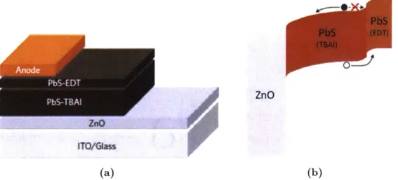
achieved via the novel technique of band alignment engineering [43]. Ligand exchange has been shown to modify the band structure of PbS quantum dots via the differing surface dipoles of the various ligands [44]. In band alignment engineering, a high absorption layer of QDs passivated with iodine ligands (PbS-TBAI) is used as the main active layer, while a thin layer of ethanedithiol functionalised dots (PbS-EDT) is deposited between this layer and the anode. EDT is chosen in order to provide a band offset as shown in Fig. 2-2b. This layer then functions as an electron blocking hole extraction layer, increasing the carrier collection efficiency by ensuring electrons do not cross into the anode and by providing a driving force for holes towards the anode. It is also postulated to reduce surface recombination at the active layer/anode interface, and slightly increases the depletion across the PbS-TBAI absorber.
When first reported, this architecture gave a 20% increase in short circuit current density (Jsc) and led to what at the time was a record cell efficiency of 8.55%. More recently, this method of band alignment engineering has been extended to include a self-assembled monolayer (SAM) of aromatic molecules functionalising the ZnO layer, as is often done in organic solar cells [45]. This is used to optimise the work function difference between the ZnO and the QD layer, improving Voc and leading to a reported cell efficiency of 10.6% [46].
However, despite the benefits of the depleted heterojunction structure and band alignment engineering, even champion QDSC devices suffer from a number of fun-damental problems which have thus far limited achievable efficiencies. The possible solutions to, and even the origins of, these issues remain an area of active research.
2.1.1
Trap
states
QD films are prone to having high densities of mid-gap states known as traps [47].
These trap states act as recombination centres where, in the example of an electron trap, an electron will fall into a lower energy state from the conduction band. It will remain trapped there until either it gets enough energy to escape, or it recombines with
PbS PbS (EDT) (TSAI) ZnO ZnO ITO/Glass (a) (b)
Figure 2-2: The (a) architecture and (b) band structure of a band alignment engineered QDSC. TBAI (tetrabutylammonium iodide) is a source of iodine ligands. The step at the EDT/TBAI interface can be seen to block the deleterious flow of electrons to the anode. ITO = indium tin oxide. Figures adapted with permission from [43].
a hole in the valence band. This energy loss is obviously detrimental to the efficiency of an energy harvesting device, and as such reducing the trap state density in QD films has been a high priority for improving efficiencies. In fact, Voc in QDSCs is in some cases limited by Fermi level pinning caused by carrier trapping [14]. Furthermore, some studies have shown that recombination is limited largely by diffusion of carriers to trap sites [14,48]. This would imply that enhancing carrier mobility in QD films would have limited benefits, as it would simply allow faster diffusion to trapped carriers and thus lead to increased recombination.
While the exact causes of traps in QDs are still a subject of some debate, it is clear that trap state density is sensitive to both the QD core structure and the ligand shell. As synthesised PbS QDs tend to deviate from stoichiometry, often being lead rich at their surfaces [47]. Computational studies have shown that bare, stoichiometric
QDs
are free from midgap states, while off stoichiometry leads to the formation of trapstates in the gap [49]. Additionally, it is well known from experimental trends that improved passivation of surface sites on QDs leads to reduced trap state density and improved device performance. Many methods have been used to move towards full pas-sivation of the dots' surfaces, including adding a paspas-sivation step during synthesis and
the use of atomic ligands which can more easily reach unpassivated surface sites [19,47]. Atomic halide ligands have seen widespread adoption and have contributed to record device performance, but whether their success is due to the passivation of surface defects or some other mechanism has remained unclear.
2.1.2
Charge extraction
The carrier collection length in PbS QD films is roughly 250nm, the sum of the minority carrier diffusion length (100nm) and the depletion width within the film
(150nm)
[50]. Carriers generated further away in the film may not be collected by thesolar cell, reducing efficiency and generated power. However, it is desirable to make the active layer of the solar cell thicker, since the photon absorption length is of the order of 1pm in the depleted heterojunction architecture with an average absorption coefficient [19]. As discussed previously, carrier diffusion length can be increased by reducing trap state density, but the impact of this is minimal compared to the large discrepancy between the collection and absorption lengths.
Exploiting the tuneable bandgap of QDs, some studies have used graded devices with QDs of different sizes, and thus different bandgaps, to create what is known as a "quantum funnel" in order to increase charge carrier diffusion [46]. However, these devices have never matched the efficiencies of the more estabilished QDPV archi-tecture, due to the difficulty in creating n-type PbS QDs with high carrier densities [51].
An alternative method is to create a bulk heterojunction structure, essentially working around the problem by decreasing the distance a charge carrier must travel before being collected. As alluded to previously in Fig. 2-1b, most depleted heterojunction
cells use nanostructured ZnO or TiO2 deposited by spin coating nanoparticles of
the oxide, but the extent of the mixing is minimal. An extension of this idea is the disordered bulk heterojunction, where the nanoparticles are blended through the active
QD
layer. This structure can be very difficult to optimise in terms of percolationheterojunctions, where interpenetrating 1D structures are leveraged to effectively decouple the collection length from the absorbing layer thickness.
Arguably the most successful of these bulk heterojunction structures has used nanowires grown from ZnO, interdigitating through the PbS layer to provide pathways for elec-tron extraction. The nanowires are grown hydrothermally from a ZnO seed layer deposited on the TCO, and can in theory be grown to arbitrary heights to allow maximum absorption of light in the PbS layer. The initial report of QDSCs based on such nanowire arrays measured a 50% enhancement in Jsc and efficiencies that
improved by 35% over the standard architecture [52]. However, even optimised
nanowire growth results in arrays that suffer from non-uniformity in length and areal density, and from overlapping and intertwining, resulting in incomplete QD infiltration and voids between wires as can be seen in Fig. 2-3. Poor length control can lead to shorting of the device, if longer nanowires touch the top electrode, while shorter wires leave larger undepleted regions in the QD film, increasing recombina-tion losses. Recently, great progress has been made in improving the uniformity by templating with e-beam lithography or growing from seed layers on graphene, but a method more suited to large scale industrial processes would still be desirable. [53-55].
Figure 2-3: SEM images of hydrothermally grown ZnO nanowires from (a) top down and (b) cross
sectional views. Viewed from above, irregularity in growth can be observed, whilst the side on view shows dark voids with no QD penetration. Reproduced with permission from [52].
pattern nanocrystal films: both ZnO, to allow for the same benefits in junction contact area afforded by ZnO NWs; and to demonstrate for the first time direct patterning of a PbS QD film, to provide a method with the potential to improve light-trapping within the device and to increase junction contact area at the anode, rather than just at the oxide interface.
2.2
Direct Nanoimprinting
Any patterning method for nanoparticle films must obviously be able to produce patterns with nanometer-scale features, as the material layers in PbS QDSCs are only on the order of 100nm thick. However, we also sought to develop a patterning method for nanoparticle films that would be intrinsically scaleable and compatible with high throughput manufacturing, as it is important that improvements in PbS
QDSC
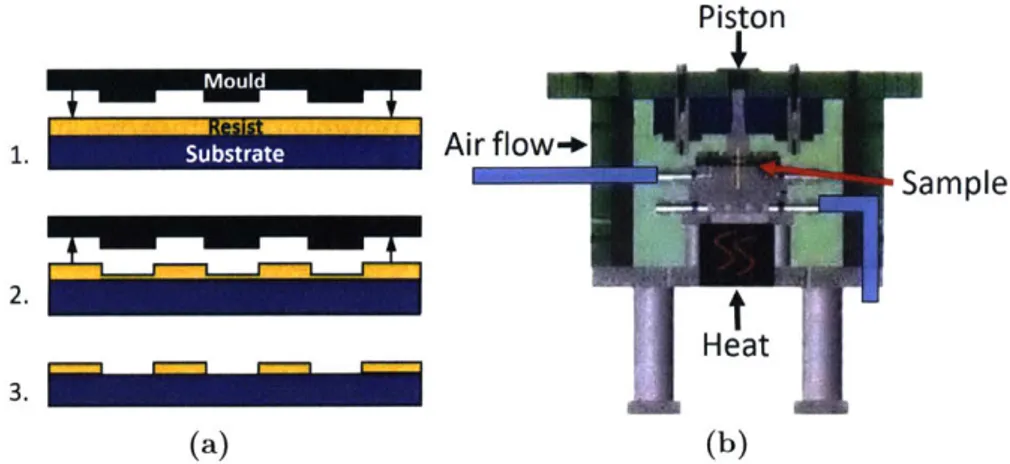
performance do not come at the expensive of their being economically viable, thus ruling out nanoscale patterning methods such as e-beam lithography that are inherently slow and expensive. With these considerations in mind, we turned to nanoimprint lithography (NIL).NIL is a high throughput, low cost lithographic technique that was first developed by S. Chou at Princeton in 1995 [56]. As with other lithographic techniques, it involves
patterning a polymer resist deposited over another material so that an etch process can be used to transfer the pattern into the underlying material. Unusually how-ever, it employs physical depression of the polymer, heated above its glass transition temperature, using a mould, as illustrated in Fig. 2-4a. This means that once a master mould with the desired nanoscale features is created, it can be reused multiple times, resulting in low overall cost. Nanoimprint lithography also is remarkably high resolution, limited only by the resolution of the technique used to create the mould, and has been used to create feature sizes as small as 6nm [57].
Piston 1. Air flow-+-Sample 2. Heat 3. (a) (b)
Figure 2-4: (a) Schematic of nanoimprint lithographic process. A patterned mould is pressed into
a polymer resist, which deforms to the mould's pattern, creating a thickness contrast. The mould is then removed and an anisotropic etch step is perfomed to create the desired pattern for transfer to the substrate. Adapted from [56]. (b) Schematic of the nanoimprint setup used in this research. Designed by T. Bloomstein, Lincoln Labs.
as any etch step will damage the QDs in the film, stripping ligands and resulting in
QD aggregation. However, the NIL process has also been adapted to imprint the
non-polymeric substrate material directly. This has been demonstrated on metals and on silicon, and is achieved by using a laser pulse to melt the material for a few hundred nanoseconds while it deforms beneath the mould [58,59]. Similarly however, laser assisted melting of the QDs in film would destroy the fragile QD surfaces, and as such is
unsuitable. PbS QDs can survive and even benefit from mild annealing - air-annealing
at 110'C has been shown to cause some beneficial oxidation, which passivates surface traps [60]. However, annealing leads to decreased particle spacing and in some cases, the decomposition of ligand molecules and partial particle sintering. The onset of this regime depends on the capping ligands. However, we can conclude that as long as the material is able to deform under the mould, it can conform to the desired pattern.
To experiment with direct nanoimprinting (DNi) of nanoparticle films, we used an adapted experimental setup that had previously been used for conventional NIL, designed by T. Bloomstein of Lincoln Labs [61]. It was adapted to provide higher pressure for the imprint process, around 1000psi, given the non-polymeric nature of the samples. It was also capable of heating the sample up to 400 C during the imprint
process, and blowing air over the sample for rapid cooling. Silicon moulds with a regular pattern of wedges with a 200nm period (see Fig. 2-5a) were used for the initial development of the DNi process due to their availability, but the process could be adapted to other patterns with similar aspect ratios. In theory, structures and dimen-sions could be optimised computationally to provide additional plasmonic absorption enhancements, but that was deemed beyond the scope of this first developmental project.
First tests of DNi on ZnO and PbS QD films showed some pattern transfer to the films, but severe delamination of the imprinted material from the substrate and complementary contamination of the mould (see Figs. 2-5b and 2-5c). For this reason, adopting a method used in polymeric NIL, we chose to functionalise the Si mould with a low stiction monolayer, using silane chemistry (see Fig. 2-5d) [62,63]. Silanes are known to bond well with activated (i.e. hydroxylated) silicon surfaces, and such reac-tions can be made self-limiting to one monolayer by choosing an appropriate tail group.
In our process, Si moulds were cleaned with organic solvents and then activated via 10mins of oxygen plasma treatment, stored in water, and then dried and put inside a vacuum flask along with a small container of perfluorooctyltrimethoxysilane (PFOX). Storage in water was found to be essential after many failed functionalisations, as it preserves the high surface energy activated surface and prevents it from reacting before being sealed in the vacuum flask. Furthermore, although the presence of excess water during the reaction prevents successful monolayer formation, the trace water left on the Si surface has been shown to dramatically increase the quality of the monolayer formed [63]. PFOX was chosen over the more typically used perfluorooctyltrichlorosi-lane to avoid the liberation of HCl during the reaction. The flask was pumped down to vacuum to vapourise the PFOX, and then left for around 2hrs for a monolayer to form on the activated Si. Although liquid-phase functionalisation would have been simpler, requiring simply leaving PFOX solvanted in ethanol on the surface of the moulds overnight, we were concerned that if future research required the imprinting
of higher aspect ratio structures, the lotus effect would prevent penetration of the solvent into the pattern and thus full functionalisation within the structures [64]. As such, we chose to spend the time optimising the vapour phase reaction.
Monolayer formation was confirmed via a contact angle decrease for water droplets on the mould's surface and a visual colour change of the patterned area from black to dark green. Incomplete functionalisation was generally visually obvious, with patches of interference-based colour change alongside black, unfunctionalised areas. However, when successful, functionalisation of the moulds drastically improved the imprint
quality, greatly reducing delamination and improving pattern transfer.
(a) (b) F F F FF F F F F F F F F F F F F FF OH OH /S\, (c) (d)
Figure 2-5: (a) Example of silicon mould. (b) ZnO film after DNi with no surface functionalisation.
Areas of film delamination are clearly evident. (c) Si mould surface afer DNi of ZnO film with no surface functionalisation. Large patches of ZnO have been removed with the mould. (d) Schematic functionalisation of Si mould surfaces.
2.3
DNi of ZnO Films
The idea of patterning the oxide layer in QDPV cells to improve light trapping has some precedent in literature. One study investigated a nanoimprint procedure on a UV-curable ZnO sol-gel, shaping the sol-gel before curing using a perfluoropolyether (PFPE) mould created from a silicon master, then applying pressure to the mould during curing, followed by additional UV curing and a 4000 C anneal. The process was used to create only sparse trench structures for the purpose of increasing interfacial area [65]. While even this modest structuring resulted in over a 50% improvement to Jsc, the multi-step nature of the process along with the limited structuring and the need for a sacrificial polymer mould meant that improvements would be necessary.
Another publication investigated the use of pyramidal periodic structures for light path folding, but focused on the conformal coating of QDs on the oxide layer to reduce interfacial recombination [66]. Simulations suggested the structures could enhance long-wavelength photon absorption to 165% of normal levels, increasing Jsc by 40%
by scattering light back through the absorbing later and increasing the interfacial
area between the oxide and QD layers. The structures were stamped from
nanopar-ticulate TiO2, avoiding the loss of the nanoporous interface, but again required a
multi-step stamping procedure involving the creation of a disposable polydimethyl-siloxane (PDMS) mould from a silicon master, a second reciprocal PDMS mould, and egregiously, an 8h contact phase where no pressure is applied and only gravity is acting on the mould. Furthermore, the aspect ratio of the pyramids was intrinsically
low, and they were fabricated multiple microns in height.
While these studies showed the potential of nanoimprinting to structure the ox-ide layer, we believed that they were unsuitable for large scale manufacturing of
QDSCs,
and furthermore that the degree of nanoscale structuring could be improved. As such, we sought to use DNi with in-situ annealing to create regular nanowedgeinterfacial area on the nanoscale and light trapping within the film demonstrated in the two aforementioned studies.
We first synthesised ZnO nanoparticles according to a previously published and well established recipe. Briefly, zinc acetate dihydrate (2.95g) was dissolved in 125ml of methanol at 60'C. Potassium hydroxide (1.48g) was dissolved in 65ml of methanol.
This was then slowly added to the zinc acetate and stirred at 600C for roughly 2.5hrs.
The ZnO nanoparticles were then extracted by centrifugation, washed with methanol, redissolved in chloroform and finally filtered through a 0.45pm filter two days later. Films were formed by spin-coating 60puL of the ZnO suspension onto a substrate, where spin speed could be used to vary the thickness and density of the final film. In general, films were coated at slower speeds that is standard in QDPV literature (1000rpm vs. 2300rpm), to provide thicker, less dense films that could more easily conform to the mould pattern. In all experiments, we used pre-patterned ITO on glass substrates prepared to the same specifications as those used in almost all QDPV cells, in order to ensure our results would be relevant to future devices.
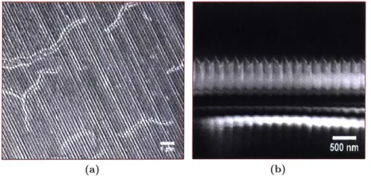
Fig. 2-6 shows the main results of the DNi process applied to ZnO films. The as deposited ZnO film shows the roughness and voids inhert in films spin coated from ZnO nanoparticles. After 1hr DNi at 200'C, regular indentation begins to appear on the surface of the film with a 200nm period, matching the tips of the mould wedges. However, the film does not conform to recognisable wedges, and increasing the time of the DNi has little effect. When performed at 300'C for 1hr, however, the wedge shape of the mould with a 200nm period can clearly be see in the ZnO film after cooling and removal of the mould.
Furthermore, the pattern transfer is regular over a large area on the order of hundreds of microns, likely limited only by irregularities in the pressure from the DNi piston system or the cleanliness of the mould. Fig. 2-7 shows an imprinted area of ZnO in a series of decreasing magnifications, to show how the quality of the features at the
(a) (b) (c)
Figure 2-6: (a) As desposited ZnO film (b) ZnO film after 1hr DNi at 200 C. (c) ZnO film after 1hr DNi at 300'C. All scale bars are 1000nm.
scale of hundreds of nanometers extends to the micron scale and beyond.
Figure 2-7: Imprinted ZnO layer using a silane functionalised mould. Repeating light and dark
contrast indicates peaks and valleys of imprinted pattern.
Unfortunately, the DNi process as applied to ZnO films has a number of draw-backs. First and foremost, the high temperature of 300'C required to form reasonable wedge structures poses many problems. It is well known that the resistance of ITO, the most commonly used transparent electrode for QDPV, increases exponentially when exposed to temperatures above 200 C [67]. This could be ameliorated by substituting FTO as the transparent electrode, which has better temperature stability, though FTO has a slightly less ideal band alignment with ZnO. Furthermore, higher temperatures can also lead to the deterioration of the SAM on the mould, increasing the likelihood
of areas of delamination and thus lost active device area (though we note that silane SAMs have significantly higher temperature stabilities than other common SAMs such as thiols) [68]. On a practical note, the 300 C anneal also had a tendancy to melt the plastic tubing to the vacuum line of the DNi equipment when air was blown over the device to cool it, necessitating ambient cooling and increasing the overall processing time, reducing hte applicability of the method to high throughput manufacturing.
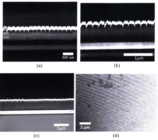
We fabricated QDPV devices on imprinted ZnO by LbL coating, via a standard procedure of PbS QD layers with the native OA ligands exchanged with iodine ligands. Briefly, for each layer, two drops of CQDs were deposited on the substrate through a 0.22pam filter and then spun at 2500rpm for 10s. For I-capped layers, the QD layer was covered with 10mg/ml TBAI in MeOH and left for 30s to exchange before being spun at 2500rpm for 30s. After each exchange, the QD layer was covered in MeOH and immediately spun at 2500rpm for 15s to wash off excess ligand molecules, with this washing step then repeated.
Unfortunately, device performance was poor, giving cells with only 1.2% PCE (see
Fig. 2-8). This was likely due to many factors - for example, poor layer uniformity
in the spin coated QD layers was observed through the poor optical quality of the final device, likely contributing to the low fill factor of these devices. This would
likely be due to a number of factors - firstly, the devices would likely benefit from
optimisation and automation of the spin coating procedure, but it is also likely that it is more difficult to coat uniform layers on ZnO films imprinted with patterns with nanoscale features. However, given the success of PbS QDPV devices deposited on ZnO nanowires, we know that this difficulty can be overcome with optimised spin coating, and though it is not clear whether this would extend to large area deposition methods such as slot die or spray coating, there is no obvious reason it would not [52].
-1 Voc (v) 0.348 JSC (mA/cm2) -10.4044 -3 FF 34.3% E 1.24% -5 -9 -11 0 0.1 0.2 0.3 Voltage (V)
Figure 2-8: Performance of PbS QDPV with imprinted ZnO, with key metrics inset.
DNi process to adapt the process to the PbS active layer and by extention, pattern the top electrode, one of the ultimate goals of this project. Our hyprothesis that the freedom of nanoparticles to move within the imprinted layer is the ultimate driver of imprint quality was borne out by our improvements in imprint quality with lower density ZnO films. Furthermore, we would expect similar or better imprint quality to
be accessible at much lower temperatures in PbS QD films, as ZnO nanoparticles are not passivated with ligands and so will tend to sinter after deposition, and thus ligand
passivated QDs in the active layer should be much more free to move. As such, we elected to apply what we had learned and focus our efforts on imprinting the active
layer rather than optimising the imprinting of ZnO, as active layer patterning had
never been demonstrated and had a greater potential impact on PCE.
2.4
DNi of PbS QD Films
In commercial silicon solar cells, micron scale surface structures are often used to improve light absorpton by the solar cell. However, engineering surface patterns in
CQD absorbing layers <300nm thick remains a challenge. As previously discussed,
patterning of the oxide layer has previously been used to improve performance. Unfor-tunely, since these techniques structure the bottom layer, the subsequent deposition