Publisher’s version / Version de l'éditeur:
Nanotechnology, 28, 27, 2017-06-14
READ THESE TERMS AND CONDITIONS CAREFULLY BEFORE USING THIS WEBSITE. https://nrc-publications.canada.ca/eng/copyright
Vous avez des questions? Nous pouvons vous aider. Pour communiquer directement avec un auteur, consultez la première page de la revue dans laquelle son article a été publié afin de trouver ses coordonnées. Si vous n’arrivez pas à les repérer, communiquez avec nous à PublicationsArchive-ArchivesPublications@nrc-cnrc.gc.ca.
Questions? Contact the NRC Publications Archive team at
PublicationsArchive-ArchivesPublications@nrc-cnrc.gc.ca. If you wish to email the authors directly, please see the first page of the publication for their contact information.
NRC Publications Archive
Archives des publications du CNRC
This publication could be one of several versions: author’s original, accepted manuscript or the publisher’s version. / La version de cette publication peut être l’une des suivantes : la version prépublication de l’auteur, la version acceptée du manuscrit ou la version de l’éditeur.
For the publisher’s version, please access the DOI link below./ Pour consulter la version de l’éditeur, utilisez le lien DOI ci-dessous.
https://doi.org/10.1088/1361-6528/aa75ab
Access and use of this website and the material on it are subject to the Terms and Conditions set forth at
Halide perovskite solar cells using monocrystalline TiO2 nanorod
arrays as electron transport layers: impact of nanorod morphology
Thakur, Ujwal kumar; Askar, Abdelrahman m; Kisslinger, Ryan; Wiltshire,
Benjamin d; Kar, Piyush; Shankar, Karthik
https://publications-cnrc.canada.ca/fra/droits
L’accès à ce site Web et l’utilisation de son contenu sont assujettis aux conditions présentées dans le site
LISEZ CES CONDITIONS ATTENTIVEMENT AVANT D’UTILISER CE SITE WEB.
NRC Publications Record / Notice d'Archives des publications de CNRC:
https://nrc-publications.canada.ca/eng/view/object/?id=51c9f7aa-03ea-43b3-b25e-a422ea6d1b2b https://publications-cnrc.canada.ca/fra/voir/objet/?id=51c9f7aa-03ea-43b3-b25e-a422ea6d1b2bNanotechnology
PAPER
Halide perovskite solar cells using monocrystalline
TiO
2
nanorod arrays as electron transport layers:
impact of nanorod morphology
To cite this article: Ujwal Kumar Thakur et al 2017 Nanotechnology 28 274001
View the article online for updates and enhancements.
Related content
Optimization of charge transfer and transport processes at the CdSe quantum dots/TiO2 nanorod interface by TiO2 interlayer passivation
O A Jaramillo-Quintero, M A Triana and M E Rincon
-Mesostructured perovskite solar cells based on highly ordered TiO2 network scaffold via anodization of Ti thin film
Aibin Huang, Jingting Zhu, Jianyun Zheng et al.
-Surface modifications of photoanodes in dye sensitized solar cells: enhanced light harvesting and reduced recombination
Vibha Saxena and D K Aswal
-Recent citations
Controllable Preparation of Rutile TiO2 Nanorods Array for Enhanced Photovoltaic Performance of Perovskite Solar Cells
Shufang Wu et al
-Tunable photovoltaic performance of preferentially oriented rutile TiO2 nanorod photoanode based dye sensitized solar cells with quasi-state electrolyte
T C Sabari Girisun et al
-Editorial—Focus on inorganic semiconductor nanowires for device applications
Adam Micolich et al
Halide perovskite solar cells using
monocrystalline TiO
2
nanorod arrays as
electron transport layers: impact of nanorod
morphology
Ujwal Kumar Thakur
1,3, Abdelrahman M Askar
1, Ryan Kisslinger
1,
Benjamin D Wiltshire
1, Piyush Kar
1and Karthik Shankar
1,2,31
Department of Electrical and Computer Engineering, University of Alberta, 9211-116 St, Edmonton, Alberta, T6G 1H9, Canada
2
NRC National Institute for Nanotechnology, 11421 Saskatchewan Dr NW, Edmonton, AB T6G 2M9, Canada
E-mail:ujwal@ualberta.caandkshankar@ualberta.ca Received 20 March 2017, revised 15 May 2017 Accepted for publication 30 May 2017 Published 14 June 2017
Abstract
This is the first report of a 17.6% champion efficiency solar cell architecture comprising monocrystalline TiO2nanorods (TNRs) coupled with perovskite, and formed using facile
solution processing without non-routine surface conditioning. Vertically oriented TNR ensembles are desirable as electron transporting layers (ETLs) in halide perovskite solar cells (HPSCs) because of potential advantages such as vectorial electron percolation pathways to balance the longer hole diffusion lengths in certain halide perovskite semiconductors, ease of incorporating nanophotonic enhancements, and optimization between a high contact surface area for charge transfer (good) versus high interfacial recombination (bad). These advantages arise from the tunable morphology of hydrothermally grown rutile TNRs, which is a strong function of the growth conditions. Fluorescence lifetime imaging microscopy of the HPSCs demonstrated a stronger quenching of the perovskite PL when using TNRs as compared to mesoporous/ compact TiO2thin films. Due to increased interfacial contact area between the ETL and
perovskite with easier pore filling, charge separation efficiency is dramatically enhanced. Additionally, solid-state impedance spectroscopy results strongly suggested the suppression of interfacial charge recombination between TNRs and perovskite layer, compared to other ETLs. The optimal ETL morphology in this study was found to consist of an array of TNRs ∼300 nm in length and ∼40 nm in width. This work highlights the potential of TNR ETLs to achieve high performance solution-processed HPSCs.
Supplementary material for this article is availableonline
Keywords: semiconductor nanowires, nanostructured titania, solvothermal synthesis, time-resolved photoluminescence, photovoltaics, single crystal nanostructured titania, Mie scattering 1. Introduction
Organometal trihalide perovskite materials with the composition ABX3 [A = Cs + , CH3NH3 + (MA), or NH=CHNH3 + (FA);
B=Pb or Sn; X=Br or I] are the focus of intense worldwide research interest for use as light-absorbing materials in photo-voltaic cells because of their outstanding optoelectronic proper-ties such as a direct optical bandgap, free carrier generation at room temperature, broadband light absorption, absence of deep level traps, ambipolar transport, and long carrier diffusion lengths Nanotechnology
Nanotechnology 28 (2017) 274001 (10pp) https://doi.org/10.1088/1361-6528/aa75ab
3
Authors to whom correspondence should be addressed.
[1–5]. In the last decade, a remarkable enhancement in the photoconversion efficiency (PCE) of perovskite solar cells has been demonstrated. Miyasaka et al reported the first perovskite solar cell in 2006 [6]with a PCE of 2.2%, which they improved to 3.8% in 2009 [7]. Intensive research into the development of HPSCs is now in progress which has led to a current highest certified PCE of 22.1% [8]. In general, certain members of the organometal trihalide perovskite semiconductor family including MAPbI3and FAPbI3have a lower effective electron diffusion
length compared to the effective hole diffusion length in solution cast thin films [9,10], an issue which one-dimensional electron transport layers (1D-ETLs) can assist with, because of which nanostructured ETLs offer the potential to enhance the perfor-mance of HPSCs [9,11,12]. The nanostructured ETL not only improves electron transport but also provides a mechanical support and a scaffold for the perovskite absorber layer in solar cells. Nanostructured ETLs could also be used to reduce ther-modynamic losses related to photons [13, 14] through incor-poration of a number of nanophotonic effects such as photonic bandgap crystals [15–18], resonant and non-resonant Mie scat-terers [19, 20], whispering gallery modes [21] and waveguide modes [22,23]. Transparent semiconducting metal oxides such as TiO2, SnO2, ZnO, SrTiO3and WO3are the most commonly
used ETL materials which ensure efficient contact with the perovskite active layer and selectively transfer photogenerated electrons to the underlying electrode while also blocking holes [24–28]. Mesoporous TiO2is the most common ETL used for
perovskite solar cells. The mesoporous architecture is comprised of a large number of ca. 20 nm-sized nanoparticles with many grain boundaries; this restricts the flow of electrons, resulting in poor charge transfer. Furthermore, the mesoporous architecture does not provide a unified path to photogenerated electron flow which leads to a random walk of electrons through the ETL [29,30]. Such a random walk-type transport increases the path length electrons must travel to the collecting electrode and increases recombination’s probability. To overcome problems associated with the mesoscopic structure, a tremendous effort is being devoted towards the application of 1D-ETLs in HPSCs. 1D-ETLs provide a direct path for photogenerated electron transport and have a large internal surface area, leading to fast charge transport, efficient charge separation and a superior charge collection efficiency. 1D-ETLs also provide better pore filling of the perovskite absorber than the nanoparticulate struc-ture in mesoscopic TiO2thin films because of their open pore
structure [31–33]. TiO2, ZnO, WO3, and CdS nanorods and
nanotubes have been tested as ETLs for perovskite solar cells, but only TiO2 nanorods (TNRs) have consistently produced
HPSCs with PCEs above 15% [34–37]. Several works on the application of TNRs as ETLs have been documented [38]. Qui et al reported TNRs sensitized using an extra thin layer of CH3NH3PbBr3 having a PCE of 4.87% [39]. Park et al
com-pared the photovoltaic performance of long (>1 μm) and short (<1 μm) TNRs, and found that the shorter nanorods provided better infiltration of perovskite. By using 560 nm long nanorods, they achieved a PCE of about 9.4% [33]. Jiang et al tried to further optimize the length of nanowires for high performance HPSCs; they found that increasing the length of nanowires to 900 nm helped improving the PCE by enhancing the short-circuit
current density, while increasing the nanowire length to 1.2 μm drastically reduced the short circuit current and open circuit voltage [40]. Recently, Li et al [36] reported perovskite solar cells with a PCE of 18.2%. They tuned the morphology of titania nanorods by using different organic acids in the growth solution of nanorods and used a UV-ozone treatment to improve the TNR/perovskite interface [36]. Unlike the use of organic acids or plasma treatment or ALD coatings on the surface, the only surface treatment employed by us was the well-established TiCl4
treatment, which is considered routine for nanostructured TiO2
[41–43]. Herein, we present an in-depth discussion of the elec-trical behavior of HPSCs based on TNR ETLs, which is essential in order to understand the sources of both underperformance and outperformance in various device parameters, so as to enable the achievement of even higher efficiencies close to the Shockley– Queisser limit [44]. We studied in depth nanorods’ effects on the optical properties of the resulting HPSCs. We demonstrated the profound effect of TNR morphology on charge separation and recombination at the perovskite/TNR interface. We optimized the morphology of hydrothermally grown rutile nanorods to produce perovskite solar cells with a champion PCE of 17.6%.
2. Experimental
2.1. Synthesis of TNRs arrays
Titanium (IV) n-butoxide (TBO), titanium (IV) isopropoxide, acetonitrile, lead iodide and lead bromide was purchased from Acros Organics. Acetic acid, HCl, formamidinium iodide (FAI), 4-tert-butylpyridine, lithium bis(trifluoromethanesulfonyl)-imide and spiro-OMeTAD were purchased from Sigma-Aldrich. Methylammonium bromide (MABr) was obtained from Dyesol. Chlorobenzene, titanium (IV) chloride, dimethylformamide (DMF) and dimethylsulfoxide (DMSO) were purchased from Fisher Scientific. Chemicals were used as received without any further purification. Fluorine-doped tin oxide (FTO) coated glass slides (Hartford Tec Glass Company) were used as substrates and were first cleaned by sonication in acetone, methanol and deionized water for 10 min each. A thin compact layer of TiO2
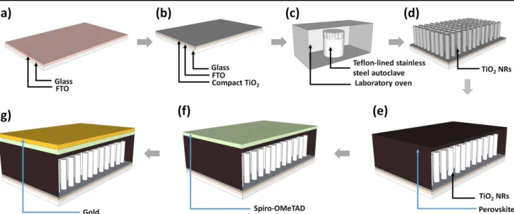
was deposited on the cleaned FTO:glass substrates (figure1(a)). The precursor solution for the deposition of compact TiO2was
prepared by a method described elsewhere; in brief, 369 μl of titanium (IV) isopropoxide and 70 μl of 1 M HCl were sepa-rately diluted in 2.53 ml of isopropanol. Diluted HCl was added drop by drop into the diluted titanium (IV) isopropoxide solution under stirring. After overnight stirring of the mixed solution, it was filtered using a 0.2 μm filter and deposited over cleaned FTO:glass substrates by spin casting at 3000 rpm for 30 s, fol-lowed by calcination at 450 °C for 30 min [45–47]. The TNR array was grown on the FTO/TiO2 substrate by a simple
hydrothermal method. 2.5 ml of HCl (37%) and 2.5 ml of glacial acetic acid were mixed with 5 ml of DI water in ambient con-ditions. The mixture was processed in a Teflon-lined stainless steel autoclave after adding the proper amount of titanium (IV) n-butoxide (TBO) into it. The substrate was placed in the autoclave at an angle such that the FTO/TiO2 side faced
growth was conducted at 200 °C for 30 min in a laboratory oven (figure1(b)). After nanorod growth, the autoclave was cooled to room temperature in ambient air; the resulting transparent nanorod array (figure1(c)) was rinsed with DI water for 2 min and dried in a stream of flowing nitrogen. The TNR array was then treated with 40 mM of TiCl4 at 70 °C for 30 min and
annealed at 500 °C for 30 min. Mesoporous TiO2 ETLs were
deposited on FTO/TiO2by spin casting followed by calcination
at 500 °C for 30 min.
2.2. Characterization
The morphologies of the TNRs and the TNR-perovskite solar cells were imaged using a Hitachi S4800 cold field emis-sion scanning electron microscope (FESEM). UV–vis–NIR spectroscopy was performed using a Perkin Elmer Lambda-1050 spectrophotometer equipped with a 100 mm integrating sphere accessory. Steady state photoluminescence (PL) spectra were collected using a Varian Cary Eclipse spectrofluorometer. Fluorescence lifetime imaging (FLIM) was performed using a Zeiss LSM 510 NLO multi-photon microscope equipped with a Ti:sapphire laser and a FLIM module consisting of a Hama-matsu RS-39 multi-channel plate detector, a filter wheel and a Becker Hickl SPC730 board for photon counting. Solid state impedance spectroscopy (SSIS) was performed in a two-elec-trode configuration using a CHI-600E potentiostat.
2.3. Device fabrication and testing
Devices were fabricated on FTO coated glass substrates (henceforth referred to as FTO:glass) having a sheet resistance of 8Ω/,. FTO:glass substrates were patterned using 35% HCl and Zn powder. The perovskite precursor solution consisted of 1 M formamidinium iodide, 1.1 M PbI2, 0.2 M MABr and
0.22 M PbBr2 in a 4:1 mixture of DMF and DMSO. The
precursor solution was stirred for 2 h at 70 °C before being
deposited on the TNRs. The perovskite solution was deposited on TNRs in a two-step procedure: first at 1000 rpm for 10 s and then at 4000 rpm for 20 s. 100 μl of chlorobenzene was drop-ped on the spinning substrate at the 15th second of the second step for rapid crystallization. Substrates were then annealed at 100 °C for 30 min (figure1(d)). A hole transporting layer was deposited by spin-casting a solution containing 35 mg of Spiro-OMeTAD mixed with 1 ml of chlorobenzene and additives, namely 4.4 mg of lithium bis(trifluoromethanesulfonyl)-imide, 14 μl of 4-tert-butylpyridine and 17.5 μl of acetonitrile; this resulted in a hole transporting layer roughly 200 nm thick (figure 1e). A 70 nm thick layer of gold was then thermally evaporated to complete the devices (figure1(f)). The current– voltage characteristics of the samples were measured using a Keithley 4200 semiconductor parameter analyzer. For solar cell testing, one sun AM 1.5 G illumination from a collimated large area solar simulator (Newport Instruments) equipped with Class A filters was used. All the photovoltaic devices were masked with a thin black mask which was used to define an active area of 2 mm×2 mm. Incident photon-to-electron conversion efficiency (IPCE, also known as external quantum yield or EQE) was measured using a home-built set-up con-sisting of a Xe arc lamp, chopper, filter-wheel, computer-controlled monochromator, calibrated silicon photodetector and optical power meter.
3. Results and discussion
The concentration of the titanium precursor, i.e. TBO, used in the hydrothermal growth process plays a crucial role in determining the morphology of grown nanorods. Figure 2 shows cross-sectional and top-view FESEM images of rutile TNR arrays grown with different concentrations of TBO. For a constant growth temperature and duration—the length,
Figure 1.Schematic illustration of perovskite solar cell fabrication based on TiO2nanorods. (a) Fluorine doped tin oxide (FTO) glass substrate. (b) Compact TiO2layer deposited overclean FTO:glass substrate. (c) Hydrothermal growth of TNRs on FTO:glass substrates in laboratory gravity convection oven at 200 °C for 1 hr. (d) Grown rutile TNR array and (e), (f), and (g) perovskite active layer, spiro-OMeTAD and gold electrode deposited over TiCl4-treated rutile nanorods respectively.
3
width, and packing density of TNRs increase with increasing TBO concentration. The dimensions of the nanorods were determined to be ∼100, 300, 650, 800 nm long and ∼20, 40, 80, 150 nm wide for 400 (A-type), 600 (B-type), 800 (C-type), 1000 (D-type) μl of TBO, respectively, as shown in figures 2(a)–(h). Both the length and packing density of the nanorods are important parameters which decide the photo-voltaic performance of the final HPSCs. Short nanorods with a large inter-rod spacing between nanorods do not provide a sufficient number and areal density of heterojunctions for charge separation because of a low roughness factor and a low surface area. A high loading of the perovskite absorber and an inter-rod spacing well below half the electron diffusion length are essential to ensure maximum transfer of photo-generated electrons from the perovskite active layer to the TNRs. On the other hand, a very long and densely packed TNR array suffers from poor infiltration of perovskite
compared to relatively shorter nanorods with larger inter-spacing [33,48–50], in addition to increasing the probability of recombination of electrons transiting through the TNRs toward the FTO electrode with holes transiting in the per-ovskite toward the Au electrode. Therefore, the morphology of nanorods must be optimized to provide a large surface area with sufficient infiltration of the active layer, while also controlling interfacial recombination.
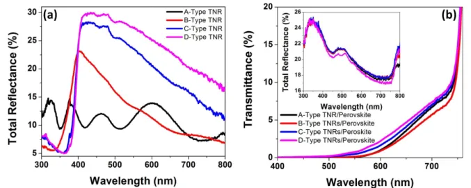
The dimensions of the nanorods also play a considerable role in their light scattering behavior which in turn, has a significant effect on the light harvesting efficiency of a solar cell. In dye sensitized solar cells (DSCs), the correct design and incorporation of Mie scatterers has been used to improve the light harvesting efficiency of near band-edge photons (∼700–750 nm) by increasing the optical path lengths of red photons inside the nanostructures [51–53]. However, DSCs consist of a 10–12 μm thick dye-coated nanostructured TiO2
Figure 2.Cross-sectional and top-view SEM images of A-type, B-type, C-type and D-type TiO2nanorod arrays grown on FTO substrate at 200 °C for 1 h using (a), (b) 400 μl (c), (d) 600 μl (e), (f) 800 μl and (g), (h) 1000 μl of titanium (IV) n-butoxide in the hydrothermal precursor solution, respectively.
film coupled to a 3–5 μm thick scattering layer which allows backscattered light from the rear of the solar cell to be effi-ciently absorbed in the rest of the dye-coated film. On the other hand, the thickness of the active layer in HPSCs is typically much smaller than 1 μm, due to which the condi-tions of scattering are different. Furthermore, in the ‘inverted’ solar cell geometry used in this study (see figure1), the TNRs are the scatterers, which are placed at the front of the solar cell rather than at the rear, due to which backscattering can actually decrease light harvesting by coupling light out of the solar cell. Therefore, forward scattering needs to be matched to the absorption of succeeding layers to improve light har-vesting. The light scattering properties of TNR arrays grown with different concentrations of TBO were studied, and are depicted in figure3. For A-type nanorods, Mie scattering is not significant and the reflectance spectrum is dominated by interference fringes (black curve in figure3(a)). The peak in the total reflectance spectrum plateaus and red-shifts as the characteristic dimension increases [20, 54–56], a behavior also observed in figure3 for TNRs of larger widths formed using increasing concentrations of TBO. Several different TiO2nanostructures with dimensions in the range 50–300 nm,
are reported to exhibit maximum back scattering at ∼400 nm [20,54–56], like that observed in figure3(a). The reflectance spectra of the perovskite-filled TNRs are shown in the inset of figure3(b) whose most obvious feature is the nearly identical values of total reflectance exhibited by each of the four nanorod morphologies investigated in this study. Since Mie scattering is a strong function of the dimensions of the nanostructures, the lack of morphology dependence is indi-cative of the dominance of specular reflection rather than diffuse reflection for the nanorod morphologies studied. Interfaces with sharp changes in the refractive index give rise to strong specular reflection. There are three such interfaces for the samples studied here: (i) the air-glass interface (ii) the glass-FTO interface and (iii) the FTO-blend film interface.
Over the UV–vis–NIR spectra range, the refractive index of glass is ∼1.5 and that of FTO is ∼2.0. As far as the TNR-perovskite blend is concerned, both the rutile phase of TiO2
and the perovskite have refractive indices of ∼2.6 over the wavelength range of interest. Therefore, strong reflections are expected from each of the aforementioned interfaces. Two prominent peaks are seen in the reflection spectra in the inset of figure 3(b), one at ∼350 nm and the other at ∼500 nm. Rutile-phase TiO2 exhibits a maximum refractive index of
3.95 at ∼330 nm and FTO:glass substrates such as those used in this study, are known to have a maximum in their reflection spectra at ∼350 nm [57]. The peak in the ultraviolet range corresponding to these maxima is clearly seen in the inset of figure 3(b). The reflectance peak at ∼500 nm is due to the perovskite exhibiting a maximum refractive index of 2.79 at ∼500 nm [58]. Figure3(b) shows that B-type TNRs blended with perovskite (red curve in figure3(b)) have the lowest total transmittance, suggesting that it would be the most efficient morphology in light harvesting.
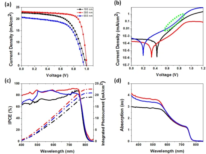
The photovoltaic performance of perovskite solar cells fabricated with different TNR types are summarized in table1 and figure S1 is available online at stacks.iop.org/NANO/28/ 274001/mmedia. The photovoltaic performance of champion cells based on A-type, B-type, and C-type nanorod morpholo-gies is shown in figure3(a), while the same for D-type TNRs is shown in figure S2. A-type nanorod arrays yielded an average PCE of 14.08%±0.70%, resulting from open circuit voltage (Voc) of 1.01 V ±0.02 V, photocurrent density (Jsc) of
21.86±1.07 mA cm−2
and fill factor (FF) of 0.64±0.02. On the other hand, B-type TNR arrays showed improvements in Jsc
and FF with corresponding improvements in PCE to 16.57%±1.04%. Upon further increasing the length of the nanorods to ∼650 nm and the width to ∼80 nm (C-type NRs), a significant decrease in Voc, Jsc, and FF was observed resulting in
the corresponding decrease in PCE to 11.74%±0.47%. The maximum Jsc obtained for B-type TNR arrays correlates well
Figure 3(a) Total reflectance (including both specular and diffuse reflectance) spectra of TiO2nanorods made with different concentrations of TBO; light is incident directly on the TNRs. (b) Total transmittance (including both direct transmission and forward scattering) spectra of TiO2 nanorod-perovskite blends with the inset showing the total reflectance of the same blends; light is incident through the FTO:glass substrate. Black, red, blue and purple colors represent A-type, B-type, C-type and D-type TiO2nanorods with lengths of 100 nm, 300 nm, 650 nm and 1000 nm respectively formed by adding 400 μl, 600 μl, 800 μl and 1000 μl of titanium (IV) n-butoxide into hydrothermal precursor solution, respectively.
5
with efficient light harvesting, as shown in figures3 and 4(d) and explained previously. Jscis proportional to IPCE which is a
product of light harvesting efficiency (ηlh), charge separation
efficiency (ηcs) and the charge collection efficiency (ηcc).
Figure4(c) shows that for all three nanorod morphologies whose IPCE action spectra are plotted, the lowest external quantum yields occur for at ∼400 nm (other than in the near band edge spectral region). High specular reflection partially explains observed phenomena for blue and UV photons, as seen in figure3(b). Another reason is that the absorption of blue and UV photons is competitive between the perovskite, the spiro-OMe-TAD, and the rutile TNR ETL, all three of which have high absorption coefficients in this spectral range. Previous reports have shown that photons absorbed by the spiro-OMeTAD layer
are not efficiently harvested and mostly lost due to recombina-tion [59]. Furthermore, while electron-hole pairs generated in the perovskite are well-separated through electron transfer to the TiO2 and hole transfer to spiro-OMeTAD following hole
dif-fusion in the perovskite layer, it is unclear if photogenerated holes in TiO2can efficiently transfer into the perovskite layer.
The high optical path lengths due to scattering within the ETL and active layer of HPSCs based on C-type TNRs, for photons with 500–600 nm wavelengths (figure 3(a)), enables improved quantum yields in this spectral range as seen in figure4(c). IPCE spectra in figure4(c) clearly show that HPSCs fabricated using B-type TNRs exhibit superior external quantum yields over the entire spectral range compared to HPSCs fabricated using other TNR morphologies.
Table 1.Photovoltaic performance of HPSCs under AM 1.5 G simulated sunlight as a function of the morphology of TiO2nanorods used as the ETL.
Morphology Voc(V) Jsc(mA cm−2) FF PCE (%) A-type Average 1.01±0.02 21.86±1.07 0.64±0.02 14.08±0.70 Champion 1.01 21.19 0.67 14.3 B-type Average 0.99±0.03 23.17±0.32 0.72±0.03 16.57±1.04 Champion 1.00 23.08 0.76 17.6 C-type Average 0.91±0.04 20.85±1.15 0.62±0.02 11.74±0.47 Champion 0.96 20.72 0.62 12.26
Figure 4.(a) Current–voltage characteristics under AM1.5 G one sun illumination. (b) Dark current–voltage characteristics plotted on a semi-log scale. (c) Action spectra showing the external quantum yields of perovskite solar cells with different TNRs. (d) UV–vis of perovskite layer over different TNRs. Black, red, and blue color represent A-type, B-type, and C-type morphologies TNRs, respectively.
Figure 4(b) compares the dark current–voltage char-acteristics of devices with different nanorod morphologies. Solar cells based on B-type TNRs (red curve in figure4(b)) exhibit the smallest dark current in the reverse bias region followed by solar cells based on A-type and C-type TNRs (black curve and blue curve, respectively, in figure4(b)). This indicates a higher shunt resistance and consequently, a better FF for solar cells based on B-type nanorods. It is apparent that decreasing the length of the nanorods increased the onset of the dark current. This implies better suppression of charge recombination in devices with smaller nanorods. Conse-quently, solar cells exhibiting the smallest dark current (red curve in figure 4(b)) also resulted in the highest PCE (see figure4(a)). In the forward bias, B-type and C-type nanorods-based solar cells exhibit a clear signature of space charge limited currents, with the green oval in figure 4(b) high-lighting the several orders of magnitude increase in the dark current for C-type nanorods. This occurs when the majority carriers (electrons) injected from the contact electrodes exceed the concentration of deep traps in the nanorods (the trap-free limit), a phenomenon well-explained by us in prior reports [60, 61]. The lowering of the equilibrium carrier concentration in the nanorods due to a high density of deep level surface traps paradoxically enables the achievement of high efficiencies by suppressing the process of back electron transfer, i.e. the recombination of electrons in the ETL with photogenerated holes in the perovskite at the TiO2-perovskite
interface. Such a deep trap-mediated suppression of interfacial recombination is maximized for a certain morphology, namely B-type nanorods with ∼300 nm long and ∼40 nm wide, as deduced from the electrical characteristics in figure4. For ∼20 nm wide A-type nanorods, the concentration of the local electric field at the needle-like NRs seen in figure2(b) produces a higher dark current due to field emission. For C-type nanorods that are ∼80 nm wide, interfacial recombi-nation is insufficiently suppressed due to the low surface-to-volume ratio, as seen in figure 2(f), and the concomitant smaller number of deep level surface traps.
As can be seen in table1and figure S2, both Vocand FF
of solar cells fabricated using C-type and D-type TNRs were significantly lower than those fabricated using A-type and B-type ones. Apart from the work functions of the electron-and hole-transporting layers, the interfacial recombination rate plays a crucial role in determining the Vocvalue [62–64].
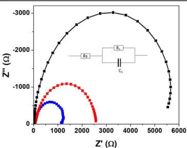
Thus, to have a better understanding on the effect of nanorod morphology on the recombination rate at the TNRs/per-ovskite interface, we performed SSIS in the dark at a forward bias of 1 V [64–68].
Nyquist plots shown in figure5 were dominated by the large semicircle for the low frequency region, while no arc for high frequency region related to perovskite/Spiro-OMeTAD was observed. An arc related to the perovskite/HTL interface is typically only observed if the TiO2 ETL thickness is
2–3 μm thick or higher [68]. Detailed analysis to calculate the recombination resistance was performed by extracting the equivalent circuit shown in the inset of figure5. Rsrepresents
the series resistance related to the connecting wires and FTO substrate. R1and C1represent the resistance and capacitance
at the interface between TNRs and the perovskite active layer, respectively. Recombination at the TiO2/perovskite interface
is inversely proportional to the recombination resistance (R1).
A higher value of R1implies a lower recombination rate at the
interface, which in turn correlates to a higher Vocand FF. In
figure5, the diameter of the arc corresponding to solar cells based on A-type TNRs is the longest, followed by that based on B-type and C-type TNRs, respectively. The recombination resistance decreased with increasing the length of the nanor-ods, which corresponds to the expected higher recombination rate for longer nanorods. This is due to the longer interaction times of electrons transiting through the nanorods with holes in the perovskite, resulting in a lower Vocand FF for the solar
cells based on longer nanorods. To compare the photovoltaic performance of TNRs with mesoporous TiO2 and
compact-layerTiO2, we prepared perovskite solar cells using
meso-porous/compact TiO2as ETLs, while other fabrication
con-ditions were kept unchanged. Figures S3, S4 and S5 show cross-sectional FESEM images of TiO2nanorods,
mesopor-ous-based, and compact-type devices, respectively. Devices using a compact TiO2layer as ETL showed an inferior PCE
of 7.46% with Jsc, Voc, and FF of 15.40 mA cm−2, 0.91 V and
0.53, respectively. Mesoporous TiO2-based devices achieved
PCE of ∼11.23%, with Voc, Jsc, and FF of 0.99 V, 19.47
mA cm−2
and 0.58, respectively. The current–voltage char-acteristics of devices with different TiO2 ETLs under AM
1.5 G solar irradiance is depicted in figure6(a). The trend of Jscobtained using different types of TiO2layers is in a good
agreement with the IPCEs in figure6(b). The IPCE values of devices with TNRs are superior to devices with mesoporous/ compact TiO2because of the enhanced charge separation and
charge carrier collection efficiencies.
To further study the charge transfer properties of differ-ent TiO2ETLs in HPSCs, steady state PL measurements were
performed. As shown in the inset of figure7, TNRs lead to a stronger quenching of the perovskite PL compared to meso-porous TiO2and compact TiO2. The same trend is observed
Figure 5.Nyquist impedance plot of solar cells with different types of nanorods, in the frequency range 1 MHz–1 Hz at a forward bias of 1 V. Black, red, and blue color represent A-type, B-type and C-type TiO2nanorods, respectively.
7
in the time-resolved PL data obtained through two-photon fluorescence lifetime imaging microscopy (FLIM), as shown in figure 7. The use of two-photon excitations enables uni-form optical excitation of the entire thickness of the per-ovskite layer, which is particularly important considering the high single-photon absorption coefficient of halide per-ovskites for supra-bandgap illumination. The PL lifetime of perovskite/TNRs was found to be smaller compared to mesoporous/compact TiO2. The time-resolved PL curves of
each sample were fitted to bi-exponential decays. The fitted parameters are summarized in table S1. Per the bi-exponential fitting, perovskite/TNR samples have faster quenching times compared to the perovskite-coated mesoporous/compact TiO2 ETLs, suggesting that TNRs extract electrons faster
from the perovskite compared to the other two types of ETLs, which is indicative of photogenerated electron-hole pairs
being well-separated in solar cells based on TNRs (through electron injection into TiO2)before geminate recombination.
Taken together, the steady-state and time-resolved PL spectra point to the superior charge separation at the TNR/perovskite interface compared to the interfaces of perovskite with mesoporous/compact TiO2 films, which also explains the
superior photovoltaic performance of solar cells based on TNRs, particularly with regards to the achieved Jsc values
(figure6).
4. Conclusion
In summary, changing the size of the nanorods by varying the concentration of the titanium source in the hydrothermal precursor solution was found to have dramatic effects on the photovoltaic performance of halide perovskite solar cells that utilize monocrystalline rutile nanorod arrays as the electron transport layer. Nanorod arrays with a width of ∼40 nm and a length of ∼300 nm outperformed other nanorod morphologies as well as mesoporous/compact TiO2in perovskite solar cells
with a champion device power conversion efficiency of 17.6%. The superior performance of these TNRs-based solar cells was mainly due to optimal light harvesting, excellent charge separation, and low interfacial recombination.
Acknowledgments
All authors thank NSERC, CMC Microsystems and NRC-NINT for direct and indirect (equipment) funding support. The infrastructure for solar cell fabrication and testing was made available through a LOF grant to KS from the Canada Foundation for Innovation (CFI) matched by the Alberta Small Equipment Grants Program (SEGP). AMA and BDW acknowledge scholarship funding from Alberta Innovates Technology Futures. PK thanks Dr Xuejun Sun at the Cell Imaging Facility for assistance with FLIM.
Figure 6.(a) Current–voltage characteristics. (b) IPCE spectra of perovskite solar cell with different TiO2underlayer. Red, wine and olive colored lines represents corresponding curves for TNRs, mesoporous TiO2, and compact TiO2, respectively.
Figure 7.FLIM spectra of perovskite on different TiO2ETLs, with the inset showing the steady state photoluminescence spectra where blue, red and black lines represent corresponding PL curves for TNRs, mesoporous TiO2, and compact (planar) TiO2respectively.
ORCID
Abdelrahman M Askar https://orcid.org/0000-0002-6092-0031
Karthik Shankar https://orcid.org/0000-0001-7347-3333 References
[1] Yin W-J, Shi T and Yan Y 2014 Unique properties of halide perovskites as possible origins of the superior solar cell performance Adv. Mater.26 4653–8
[2] Tanaka K, Takahashi T, Ban T, Kondo T, Uchida K and Miura N 2003 Comparative study on the excitons in lead-halide-based perovskite-type crystals CH3NH3PbBr3 CH3NH3PbI3Solid State Commun.127 619–23 [3] Frost J M, Butler K T, Brivio F, Hendon C H,
van Schilfgaarde M and Walsh A 2014 Atomistic origins of high-performance in hybrid halide perovskite solar cells Nano Lett.14 2584–90
[4] Askar A M and Shankar K 2016 Exciton binding energy in organic-inorganic tri-halide perovskites J. Nanosci. Nanotechnol.16 5890–901
[5] De Wolf S, Holovsky J, Moon S-J, Löper P, Niesen B, Ledinsky M, Haug F-J, Yum J-H and Ballif C 2014 Organometallic halide perovskites: sharp optical absorption edge and its relation to photovoltaic performance J. Phys. Chem. Lett.5 1035–9
[6] Kojima A, Teshima K, Shirai Y and Miyasaka T 2007 Novel photoelectrochemical cell with mesoscopic electrodes sensitized by lead-halide compounds (5) ECS Meeting Abstracts MA2007-02 352
[7] Kojima A, Teshima K, Shirai Y and Miyasaka T 2009 Organometal halide perovskites as visible-light sensitizers for photovoltaic cells J. Am. Chem. Soc.131 6050–1 [8] Green M A, Emery K, Hishikawa Y, Warta W, Dunlop E D,
Levi D H and Ho-Baillie A W Y 2017 Solar cell efficiency tables (version 49) Prog. Photovolt.25 3–13
[9] Edri E, Kirmayer S, Henning A, Mukhopadhyay S, Gartsman K, Rosenwaks Y, Hodes G and Cahen D 2014 Why lead methylammonium tri-iodide perovskite-based solar cells require a mesoporous electron transporting scaffold (but not necessarily a hole conductor) Nano Lett.14 1000–4 [10] Eperon G E, Stranks S D, Menelaou C, Johnston M B,
Herz L M and Snaith H J 2014 Formamidinium lead trihalide: a broadly tunable perovskite for efficient planar heterojunction solar cells Energy Environ. Sci.7 982–8 [11] Xing G, Mathews N, Sun S, Lim S S, Lam Y M, Graetzel M,
Mhaisalkar S and Sum T C 2013 Long-range balanced electron- and hole-transport lengths in organic-inorganic CH3NH3PbI3Science342 344–7
[12] Stranks S D, Eperon G E, Grancini G, Menelaou C, Alcocer M J P, Leijtens T, Herz L M, Petrozza A and Snaith H J 2013 Electron-hole diffusion lengths exceeding 1 micrometer in an organometal trihalide perovskite absorber Science342 341–4
[13] Polman A and Atwater H A 2012 Photonic design principles for ultrahigh-efficiency photovoltaics Nat. Mater.11 174–7
[14] Cui Y, van Dam D, Mann S A, van Hoof N J J,
van Veldhoven P J, Garnett E C, Bakkers E P A M and Haverkort J E M 2016 Boosting solar cell photovoltage via nanophotonic engineering Nano Lett.16 6467–71
[15] Lin J, Liu K and Chen X F 2011 Synthesis of periodically structured titania nanotube films and their potential for photonic applications Small7 1784–9
[16] Yip C T, Huang H T, Zhou L M, Xie K Y, Wang Y, Feng T H, Li J S and Tam W Y 2011 Direct and seamless coupling of
TiO2nanotube photonic crystal to dye-sensitized solar cell: a single-step approach Adv. Mater.23 5624–8
[17] Guo M, Xie K Y, Lin J, Yong Z H, Yip C T, Zhou L M, Wang Y and Huang H T 2012 Design and coupling of multifunctional TiO2nanotube photonic crystal to
nanocrystalline titania layer as semi-transparent photoanode for dye-sensitized solar cell Energy Environ. Sci.5 9881–8 [18] Zhang X, Han F, Shi B, Farsinezhad S, Dechaine G P and
Shankar K 2012 Photocatalytic conversion of diluted CO2into light hydrocarbons using periodically modulated multiwalled nanotube arrays Angew. Chem., Int. Ed.51 12732–5 [19] Muskens O L, Diedenhofen S L, Kaas B C, Algra R E,
Bakkers E P A M, Gómez Rivas J and Lagendijk A 2009 Large photonic strength of highly tunable resonant nanowire materials Nano Lett.9 930–4
[20] Boppella R, Mohammadpour A, Illa S, Farsinezhad S, Basak P, Shankar K and Manorama S V 2016 Hierarchical rutile TiO2 aggregates: a high photonic strength material for optical and optoelectronic devices Acta Mater.119 92–103
[21] Grandidier J, Callahan D M, Munday J N and Atwater H A 2011 Light absorption enhancement in thin-film solar cells using whispering gallery modes in dielectric nanospheres Adv. Mater.23 1272–6
[22] Mohammadpour A, Waghmare P R, Mitra S K and Shankar K 2010 Anodic growth of large-diameter multipodal TiO2 nanotubes ACS Nano4 7421–30
[23] Mohammadpour A and Shankar K 2010 Anodic TiO2 nanotube arrays with optical wavelength-sized apertures J. Mater. Chem.20 8474–7
[24] Liu D and Kelly T L 2014 Perovskite solar cells with a planar heterojunction structure prepared using room-temperature solution processing techniques Nat. Photon.8 133–8 [25] Yeom E J, Shin S S, Yang W S, Lee S J, Yin W, Kim D,
Noh J H, Ahn T K and Seok S I 2017 Controllable synthesis of single crystalline Sn-based oxides and their application in perovskite solar cells J. Mater. Chem. A5 79–86
[26] Ke W et al 2015 Low-temperature solution-processed tin oxide as an alternative electron transporting layer for efficient perovskite solar cells J. Am. Chem. Soc.137 6730–3 [27] Bhande S S, Ambade R B, Shinde D V, Ambade S B,
Patil S A, Naushad M, Mane R S, Alothman Z A, Lee S-H and Han S-H 2015 Improved photoelectrochemical cell performance of tin oxide with functionalized
multiwalled carbon nanotubes–cadmium selenide sensitizer ACS Appl. Mater. Interfaces7 25094–104
[28] Jiang Q, Zhang L, Wang H, Yang X, Meng J, Liu H, Yin Z, Wu J, Zhang X and You J 2016 Enhanced electron extraction using SnO2for high-efficiency planar-structure HC(NH2)2PbI3 -based perovskite solar cells Nat. Energy2 16177
[29] Nelson J 1999 Continuous-time random-walk model of electron transport in nanocrystalline TiO2electrodes Phys. Rev.B59 15374–80
[30] van de Lagemaat J and Frank A J 2001 Nonthermalized electron transport in dye-sensitized nanocrystalline TiO2 films: transient photocurrent and random-walk modeling studies J. Phys. Chem. B105 11194–205
[31] Feng X, Zhu K, Frank A J, Grimes C A and Mallouk T E 2012 Rapid charge transport in dye-sensitized solar cells made from vertically aligned single-crystal rutile TiO2nanowires Angew. Chem., Int. Ed.51 2727–30
[32] Law M, Greene L E, Johnson J C, Saykally R and Yang P 2005 Nanowire dye-sensitized solar cells Nat. Mater.4 455–9 [33] Kim H-S, Lee J-W, Yantara N, Boix P P, Kulkarni S A,
Mhaisalkar S, Grätzel M and Park N-G 2013 High efficiency solid-state sensitized solar cell-based on submicrometer rutile TiO2nanorod and CH3NH3PbI3perovskite sensitizer Nano Lett.13 2412–7
[34] Mahmood K, Swain B S, Kirmani A R and Amassian A 2015 Highly efficient perovskite solar cells based on a
9
nanostructured WO3-TiO2core–shell electron transporting material J. Mater. Chem. A3 9051–7
[35] Gu Z, Chen F, Zhang X, Liu Y, Fan C, Wu G, Li H and Chen H 2015 Novel planar heterostructure perovskite solar cells with CdS nanorods array as electron transport layer Sol. Energy Mater. Sol. Cells140 396–404
[36] Li X, Dai S-M, Zhu P, Deng L-L, Xie S-Y, Cui Q, Chen H, Wang N and Lin H 2016 Efficient perovskite solar cells depending on TiO2nanorod arrays ACS Appl. Mater. Interfaces8 21358–65
[37] Mahmood K, Swain B S and Amassian A 2015 16.1% efficient hysteresis-free mesostructured perovskite solar cells based on synergistically improved ZnO nanorod arrays Adv. Energy Mater.5 1500568
[38] Thakur U, Kisslinger R and Shankar K 2017 One-dimensional electron transport layers for perovskite solar cells
Nanomaterials7 95
[39] Qiu J, Qiu Y, Yan K, Zhong M, Mu C, Yan H and Yang S 2013 All-solid-state hybrid solar cells based on a new organometal halide perovskite sensitizer and one-dimensional TiO2nanowire arrays Nanoscale5 3245–8 [40] Jiang Q, Sheng X, Li Y, Feng X and Xu T 2014 Rutile TiO2
nanowire-based perovskite solar cells Chem. Commun.50 14720–3
[41] O’Regan B C, Durrant J R, Sommeling P M and Bakker N J 2007 Influence of the TiCl4treatment on nanocrystalline TiO2films in Dye-sensitized solar cells: II. Charge density, band edge shifts, and quantification of recombination losses at short circuit J. Phys. Chem. C111 14001–10
[42] Bandara J, Shankar K, Basham J, Wietasch H, Paulose M, Varghese O K, Grimes C A and Thelakkat M 2011 Integration of TiO2nanotube arrays into solid-state dye-sensitized solar cells Eur. Phys. J. Appl. Phys.53 20601 [43] Meen T-H, Jhuo Y-T, Chao S-M, Lin N-Y, Ji L-W, Tsai J-K,
Wu T-C, Chen W-R, Water W and Huang C-J 2012 Effect of TiO2nanotubes with TiCl4 treatment on the photoelectrode of dye-sensitized solar cells Nanoscale Res. Lett.7 579 [44] Shockley W and Queisser H J 1961 Detailed balance limit of
efficiency of p‐n junction solar cells J. Appl. Phys.32 510–9 [45] Yang B et al 2015 Perovskite solar cells with near 100%
internal quantum efficiency based on large single crystalline grains and vertical bulk heterojunctions J. Am. Chem. Soc. 137 9210–3
[46] Ball J M, Lee M M, Hey A and Snaith H J 2013 Low-temperature processed meso-superstructured to thin-film perovskite solar cells Energy Environ. Sci.6 1739–43 [47] Chaudhary D K, Kumar P and Kumar L 2016 Evolution in
surface coverage of CH3NH3PbI3−XClXvia heat assisted solvent vapour treatment and their effects on photovoltaic performance of devices RSC Adv.6 94731–8
[48] Liu H, Huang Z, Wei S, Zheng L, Xiao L and Gong Q 2016 Nano-structured electron transporting materials for perovskite solar cells Nanoscale8 6209–21
[49] Tétreault N and Grätzel M 2012 Novel nanostructures for next generation dye-sensitized solar cells Energy Environ. Sci.5 8506–16
[50] Fakharuddin A, Di Giacomo F, Ahmed I, Wali Q, Brown T M and Jose R 2015 Role of morphology and crystallinity of nanorod and planar electron transport layers on the performance and long term durability of perovskite solar cells J. Power Sources283 61–7
[51] Cui Y, He X, Zhu M and Li X 2017 Preparation of anatase TiO2microspheres with high exposure (001) facets as the light-scattering layer for improving performance of dye-sensitized solar cells J. Alloys Compd.694 568–73 [52] Yu H, Pan J, Bai Y, Zong X, Li X and Wang L 2013
Hydrothermal synthesis of a crystalline rutile TiO2nanorod
based network for efficient dye‐sensitized solar cells Chem. Euro. J.19 13569–74
[53] Hore S, Vetter C, Kern R, Smit H and Hinsch A 2006 Influence of scattering layers on efficiency of dye-sensitized solar cells Sol. Energy Mater. Sol. Cells90 1176–88
[54] Zhang H, Yu H, Han Y, Liu P, Zhang S, Wang P, Cheng Y and Zhao H 2011 Rutile TiO2microspheres with exposed nano-acicular single crystals for dye-sensitized solar cells Nano Res.4 938–47
[55] Peng J-D, Lee C-P, Velayutham D, Suryanarayanan V and Ho K-C 2015 Dye-sensitized solar cells containing mesoporous TiO2spheres as photoanodes and methyl sulfate anion based biionic liquid electrolytes J. Mater. Chem. A3 6383–91
[56] Huo J, Hu Y, Jiang H, Huang W and Li C 2014 SnO2 nanorod@TiO2hybrid material for dye-sensitized solar cells J. Mater. Chem.A2 8266–72
[57] Varghese O K, Paulose M and Grimes C A 2009 Long vertically aligned titania nanotubes on transparent conducting oxide for highly efficient solar cells Nat. Nanotechnol.4 592–7
[58] Löper P, Stuckelberger M, Niesen B, Werner J, Filipič M, Moon S-J, Yum J-H, Topič M, De Wolf S and Ballif C 2015 Complex refractive index spectra of CH3NH3PbI3perovskite thin films determined by spectroscopic ellipsometry and spectrophotometry J. Phys. Chem. Lett.6 66–71
[59] Wang X, Li Z, Xu W, Kulkarni S A, Batabyal S K, Zhang S, Cao A and Wong L H 2015 TiO2nanotube arrays based flexible perovskite solar cells with transparent carbon nanotube electrode Nano Energy11 728–35 [60] Mohammadpour A, Farsinezhad S, Wiltshire B D and
Shankar K 2014 Majority carrier transport in single crystal rutile nanowire arrays Phys. Status Solidi RRL8 512–6 [61] Mohammadpour A, Wiltshire B D, Zhang Y, Farsinezhad S,
Askar A M, Kisslinger R, Ren Y, Kar P and Shankar K 2017 100-fold improvement in carrier drift mobilities in alkanephosphonate-passivated monocrystalline TiO2 nanowire arrays Nanotechnology28 144001
[62] Yan W, Li Y, Ye S, Li Y, Rao H, Liu Z, Wang S, Bian Z and Huang C 2016 Increasing open circuit voltage by adjusting work function of hole-transporting materials in perovskite solar cells Nano Res.9 1600–8
[63] Suarez B, Gonzalez-Pedro V, Ripolles T S, Sanchez R S, Otero L and Mora-Sero I 2014 Recombination study of combined halides (Cl, Br, I) perovskite solar cells J. Phys. Chem. Lett.5 1628–35
[64] Mora-Seró I, Giménez S, Fabregat-Santiago F, Azaceta E, Tena-Zaera R and Bisquert J 2011 Modeling and characterization of extremely thin absorber (eta) solar cells based on ZnO nanowires Phys. Chem. Chem. Phys.13 7162–9 [65] Mali S S, Shim C S, Park H K, Heo J, Patil P S and Hong C K
2015 Ultrathin atomic layer deposited TiO2for surface passivation of hydrothermally grown 1D TiO2nanorod arrays for efficient solid-state perovskite solar cells Chem. Mater.27 1541–51
[66] Lv M, Dong X, Fang X, Lin B, Zhang S, Xu X, Ding J and Yuan N 2015 Improved photovoltaic performance in perovskite solar cells based on CH3NH3PbI3 films fabricated under controlled relative humidity RSC Adv.5 93957–63 [67] Mora-Sero I, Gimenez S, Fabregat-Santiago F, Azaceta E,
Tena-Zaera R and Bisquert J 2011 Modeling and characterization of extremely thin absorber (eta) solar cells based on ZnO nanowires Phys. Chem. Chem. Phys.13 7162–9 [68] Kim H-S, Mora-Sero I, Gonzalez-Pedro V,
Fabregat-Santiago F, Juarez-Perez E J, Park N-G and Bisquert J 2013 Mechanism of carrier accumulation in perovskite thin-absorber solar cells Nat. Commun.4 2242